Week | 7
Electronics Design
How I’m redesigning the Hello Board by adding extra components, testing and programming it.
06 March 2018 00:36:
Eagle Installation and Setup
1 - Install Eagle.
Eagle is a software to design schematics and PCBS for electronics;
2 - Import Fab Library, by copying this file to the lbr folder created on your computer inside Eagle’s directory. The Fab Library is a list of components to be used as a source library at Eagle, with the current “inventory” of recurrent components used at fab academy;
3 - Open a new Project at Eagle;
4 - Create New Schematic and Board;
5 - Search online for datasheets about each component of your board. By doing so you can understand the Pin configuration (where each pin is located on the component) and the Pins description (the functionality of each pin). Here’s the documentation of some of the parts used at the Hello Board:
ATtiny 44 | AVR ISP 6-Pin Header | FTDI SMD Header
With all the stages above completed, I’ve moved to next stage.
Designing/Redrawing the board
1 - Add the components. On Eagle’s schematic mode, using the previously installed FAB library, add each component present on the drawing below to your schematic:

R1 10k means:
R = Resistor
Quantity: 1. Value: 10k
A resistor is a component used to, literally, “resist” the current and reduce its flow.
This is the one you should look for at the Fab Library:

C1 1uf means:
C = Capacitor (in this case UNPOLARISED!)
Quantity: 1. Value: 1uf
A capacitor is like a cistern in which you store smal quantities of water or, in this case, current.
This is the one you should look for at the Fab Library:

XTAL 1 20 MHz means:
Crystal
Quantity: 1. Value: 20mhz
(This should be a resonator. The Crystal has the same image as resonator, the resonator itself is not available in the FAB library for Eagle, so you use the image of the Crystal as a placeholder). Add the 20 MHz value to the component.
This is the one you should look for at the Fab Library:

IC1 t44 means:
IC = Integrated Circuit
Quantity: 1
Type: t44 (ATtiny44)
This is the one you should look for at the Fab Library:

J1 ISP means:
J = The letter J here seems to be random and just to label a different component. 1 means, the first component of the “J” list. In this case, what really describes the component is the ISP, which is a pin header.
ISP means “In System Programmer”, and this component is the header that will connect the FabISP to our new Hello Board.
This is the one you should look for at the Fab Library:

J2 FTDI means:
J = The letter J here seems to be random and just to label a different component. 2 means, the second component of the “J” list. In this case, what really describes the component is the FTDI.
FTDI means Future Technology Devices International - The company that makes a special usb cable and the drivers which enable writing to the 6 pin output like a standard serial port. In this case we are using the pin header, in which we will connect the FTDI cable.
This is the one you should look for at the Fab Library:

2 - Position all components. On Eagle’s board mode, position all components according to drawing above, so you have a similar configuration/position.
3 - Connect the components. By combining the information you have at the boards’ drawing, the datasheets and the schematics you have just created, connect the components by naming and labelling each connection. For an instance: The pin PB3 from the microcontroller is connected to the RESET. And so is the 5th pin of the ISP header and one end of the resistor. All of them should be named (and labelled) as RESET. You can do this by:
- Clicking on the green button on the menu called “NET (draw an electrical connection)” and the draw a line connected to the pin/component;
- Right-clicking at the end of the green line and choose “Name”, to rename the connection as “RESET”;
- Right-clicking again at the end of the connection and choose “Label”, so you can see the name you’ve just input.


Do this for all components that have a connection.
4 - Do a Design Rules check. This is where Eagle will verify if the physical layout of your board layout satisfies a series of recommended parameters, called “design rules”. One parameter changed here should be the clearance (which is the distance between components). Since our smallest tool for milling is 1/64, I needed to change the size of the path to 16 mil in the clearance.

*** Tips:
You can define the Grid (ideally to a ratio of the clearance) so that its easier to move around components when distributing them in the board.

Use the Measure tool to measure the board, so that you have an idea of the size.

So, with this, I had done the basic setup of the Hello Board. Then, I’ve moved to the next stage, which is to add components that I would use for this week’s assignment, which was to add (at least) a button and LED (with a current-limiting resistor).
Adding extra components
As done for the previous components, I’ve added them on the schematics and positioned them on the board mode.
LED
Quantity: 1.
A LED is a diode that emits light. A diode is a component that allows an electric current to flow easily in one direction, but strongly restricts current from flowing in the opposite direction. The LED (Light Emitting Diode) emits light by exploiting a property called “luminescence”, where passing an electric current through certain materials cause them to emit light.
This is the one you should look for at the Fab Library:

Another Resistor
Quantity: 1.
This resistor is for the LED, so it doesn’t burn.
This is the one you should look for at the Fab Library:
NOTE: HOW TO CALCULATE THE VALUE OF THE RESISTOR:
In order to know the value of the resistor that goes with that LED, I’ve noted the reference from fablab’s inventory:

So, my LED is the 160-1169-1-ND.
Then I went to www.digikey.com and looked at the properties of it:

So, my LED has a voltage of 2.1V and a current of 10mA.
The board’s voltage is 5 volts, so, I need to use a resistor to reduce it to 2.1 v before it reaches de LED.
Then I used this formula to calculate the resistance: Voltage (v) = Intensity (A) x Resistance (ohms)
- So, my Voltage should be: 5 (the boards voltage) - 2.1 (the Voltage needed for the led) = 2.9 v
- The current Intensity needed for the LED is = 10mA. Converting to A (Amps, instead of milliamps ) = 0.01 A
(5 - 2.1) v = 0.01 A x R
2.9v / 0.01 A = R
R = 290 ohms
So, I need a 290 ohms resistor connected to my LED. Therefore, I will use 499 ohms resistor and input this value on my EAGLE design. Alternatively, you could use an OHMS Law Online Calculator, like this one:

6mm Button Switch
Quantity: 1.
This is the one you should look for at the Fab Library:

With all components added, you need to route them.
Routing the board
If you have already connected your components on the Schematics, your board will now have yellow “airwires” connecting them. So, routing is basically replacing those airwires for routes where will be the copper traces, that will physically enable all these connections. It’s like solving a puzzle, making sure that all connections are completed, without overlapping traces and vias (if the board has two sides, which is not the case here).
Using the Route tool, just connect the components according to the “airwires”.

The routing should automatically respect the parameters created during the design rules check described above. It’s also recommended to perform Design Rule Checks before, during and after the routing process.
This Sparkfun’s tutorial is helpful to explain how does Routing works.
After the routing, these were my final Schematic and Board:


Exporting the board design
You should now export the board as an image, so that you can mill it. I have already documented the stages of the milling process here on week 4.
With the board mode selected at Eagle:
1 - Go to Layer Settings and select only the top layer.
2 - Then, choose: File>Export>Image.
3 - At the export window, choose where you want to save your file, the resolution (the more the better, I have chosen 1000 dpi) and the collor settings should be MONOCHROME which will export a image with white traces. Export the image.

Note: I had an issue while exporting the png of the board. My file was being exported with its size exactly doubled. I realized this was a known bug, here’s a forum discussion about it. The work around that I’ve done was to open the exported PNG on Photoshop and change the image size, to the right size. Basically, when you set the export up in EAGLE, before you click OK, it shows you the intended output resolution (which is the correct one), so I have taken note of the X size and then, in Photoshop, I have changed the X size (making sure the aspect ratio is locked). It worked for me.
4 - Since the export PNG from EAGLE is either the size of the “window” or “full” (according to what you have chosen), you have now to open the image on photoshop and crop accordingly, so that there is only a reasonable amount of space around the board. This, cropped file, would be your “traces” file for the milling. I also use this stage to minimally customize my board by adding the circles you see on the top left corner. Then, I’ve used this file in FabModules to generate de .rml file for printing.
Traces file:

And the milled board:

5 - Using the same file generated for the traces, create the “interior” file, which is the file that will cut the board from the FR-1 board. You should do this by simply creating an white square where you want the board to be cut. This will generate a file of a white square with a black border. Make sure the width of the border is 0.79 mm as a minimum, otherwise the milling machine will not be able to cut it. Then, I’ve used this file in FabModules to generate de .rml file for printing.
Interior file:

And the milled/cut board:

Here’s the final board and its components:

Note: In the picture above there is a crystal instead of a resonator. I had mistakenly switched these and had to un-solder the crystal and re-solder a resonator later in the soldering stage.
Stuffing the board
I have, then, soldered all the components of the board, using the schematics as a “map”. I have already documented some of the soldering process here on week 4.
Here’s a video with part of the soldering process. I have spent more time double checking the info on my computer, rather than actually soldering the components :) :
And here’s the final board:


Doing a Continuity Test
A continuity test is the checking if a current flows between two points, according to the designed circuit.
So, with a Multimeter set to continuity mode (look for a diode symbol with propagation waves around it), you place one end in the first point and another end in the second point you want to measure. If there is a beep, it means that there is conductivity. If it doesn’t beep, the circuits aren’t connected.
Following my board drawing (again below), I have tested all the points that should be connected in the circuit, first by checking conductivity between all GROUND points, then VOLTAGE (VCC) and then every specific connection, such as MOSI, MISO, RESET, etc.

All worked as expected and I could even see the LED lighting up powered by the small current created by the multimeter:

Bootloading / Preparing the board for programming
This is what I have used in order to setup the Hello Board for programming:
HARDWARE
1 - AN AVRISP2 or a FabISP. I started using my previously done FabISP in-system programmer:

But then moved to using a AVRISP2 for the Bootloading, because I was getting a “pipe stalled error” while trying to bootload. My FabISP board also had a couple of resistors I forgot to remove before using it as a programmer. I did it afterwards.
2 - A 2x3 pin ISP ribbon cable, which I have produced at the lab. This was used to connect the FabISP to the Hello Board.

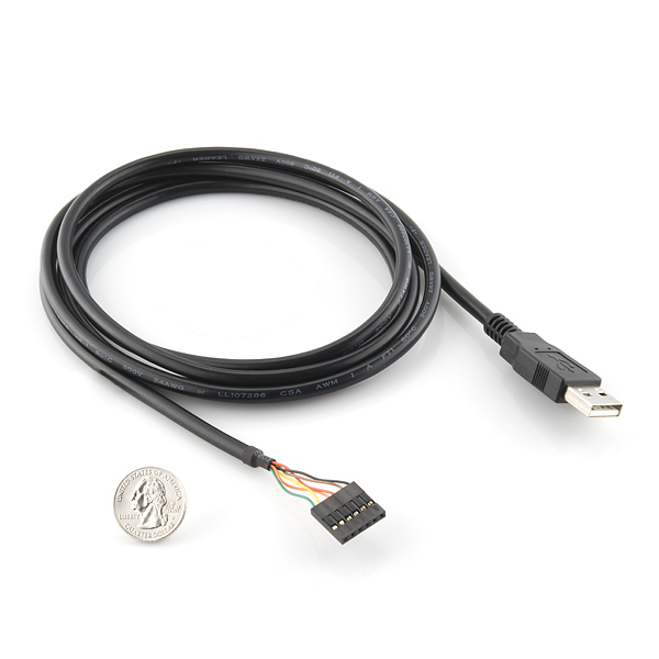
3 - A FTDI USB cable (USB -> 1x6 pin FTDI header). This was used to connect the Hello Board to the computer and power it.
Note: Needless to say that one has to be really careful when connecting the cables to the pins. Make sure you have your grounds and vccs cables connected to the right pins.
SOFTWARE
1 - The FTDI D2XX drivers for MAC. Followed installation instructions on the readme.txt file that comes along with the downloaded files.

2 - Crosspack for AVR Development
3 - Arduino
FILES
1 - hello.ftdi.44.echo.c
2 - hello.ftdi.44.echo.c.make
Connection Steps
1 - Connect computer and FabISP board via USB;
2 - Connect computer and Hello Board via FTDI USB cable (black is ground);
3 - Connect FabISP board and Hello Board together via ISP Ribbon Cable;
4 - Plug FTDI cable into board;

To make sure all boards are correctly connected to your computer, you can check the USB Ports on terminal using the following command:
system_profiler SPUSBDataType

Step by Step to Bootload
1 - On terminal, go into the directory where you have saved your hello.ftdi.44.echo.c
and hello.ftdi.44.echo.c.make files and type:
make -f hello.ftdi.44.echo.c.make

2 - Then type:
If using the FabISP as a programmer:
make -f hello.ftdi.44.echo.c.make program-usbtiny
If using the AVRISP2 as a programmer:
make -f hello.ftdi.44.echo.c.make program-avrisp2

3 - Then type:
If using the FabISP as a programmer:
make -f hello.ftdi.44.echo.c.make program-usbtiny-fuses
If using the AVRISP2 as a programmer:
make -f hello.ftdi.44.echo.c.make program-avrisp2-fuses

The board is now ready to be programmed.
Programming the board
1 - Install the ATtiny support on Arduino.
On the Arduino software, I have followed this tutorial to install the ATtiny support via Arduino’s built-in boards manager. I have found the ATtiny support through a google search that led me to the developer’s repository here.
2 - Set the Parameters
On Arduino’s menu, go to >Tools and set:
Board to “ATtiny 44”;
Processor to “ATtiny44”:
Clock to “External 20 MHz”;
Port to the port where your Hello Board is connected;
Programmer to “USBTinyISP” or “AVR ISP”.
And select “Burn Bootloader”.

PROGRAMMING TEST 1
Making the LED blink intermittently: On Arduino go to Files>Examples>01.Basics>Blink and add the PIN Position for the LED (PIN 7 in the ATTiny Microcontroller).
Here’s a screenshot of Arduino’s example and the changes written:

And a video with the result:
PROGRAMMING TEST 2
Making the LED light up when the button is pushed: On Arduino go to Files>Examples>Digital>Button and add the PIN Position for the LED (PIN 7 in the ATTiny Microcontroller).
Here’s a screenshot of Arduino’s example and the changes written, I have also changed so that the LED is ON when the Button is pushed:

And a video with the result:
These 2 documentation websites were very helpful during this process: Site 1,Site 2.