Week 6: Electronics design
This week we followed the Electronics Design class (see video here)
This page is about the individual assignment.
- Design with KiCAD
- Design with Eagle
- Board production and test
- Lab test equipment (group assignment)
- Lessons learned
- Next steps
Design with KiCAD
KiCAD is an Open Source / Free software tool for electronics design.
The process to design a boad in KiCAD goes trough few steps:
- Design the schematic
- Generate the Net list and assign a footprint to each component
- Create a PCB layout from the net list
- Export the PCB layout
In KiCAD even if not explicitly visible is important the concept of Net list. KiCAD is composed of separate tools working together. In this context the Net list is the information file that gets exchanged between tools.
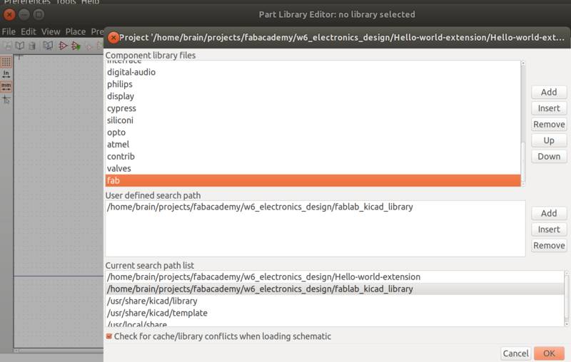
Before starting to work on a design we import in KiCAD the library of specific components used by fablab.
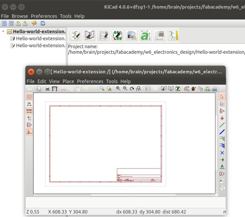
We start the project from an empty schematic
It is useful to know in KiCAD that at any time by pressing the ? key a list of shortcuts with all the associated commands appear, which is useful especially for beginners.
We start placing components searching in the library, eventually adding labels and connecting wires in the diagram.
It is also recommended in KiCAD to place air wire terminator to non used pins. By pressing the Annotate button we can give unique names to each component (this will be useful at a later stage).
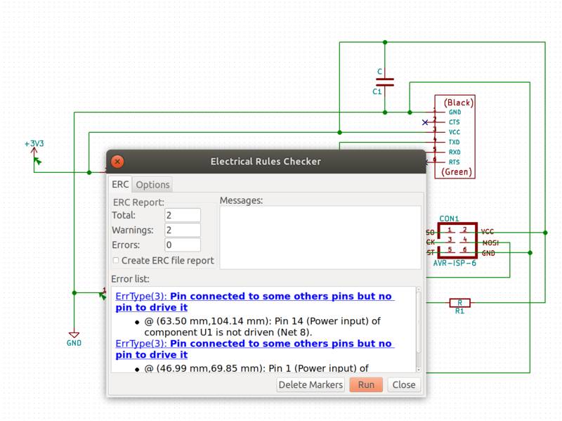
When done we can run the schematics rule checker:
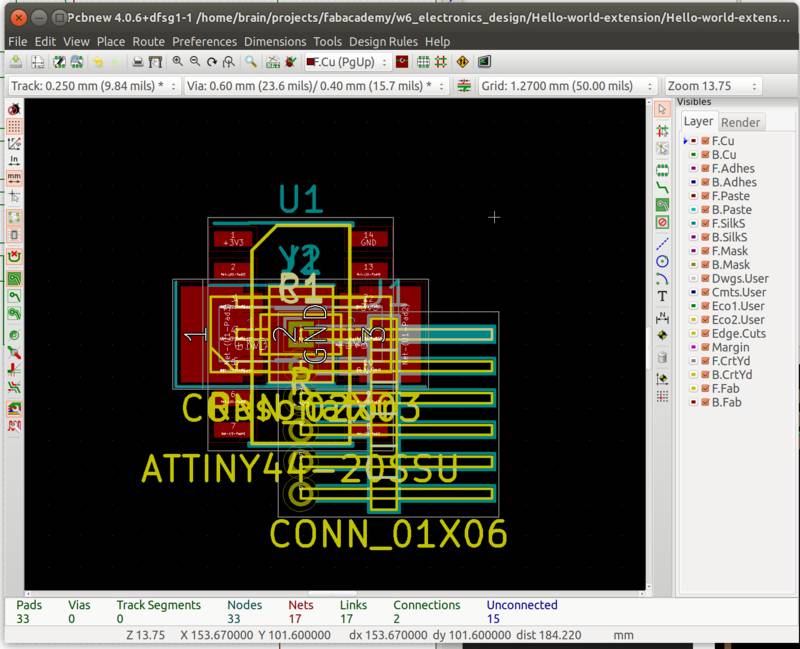
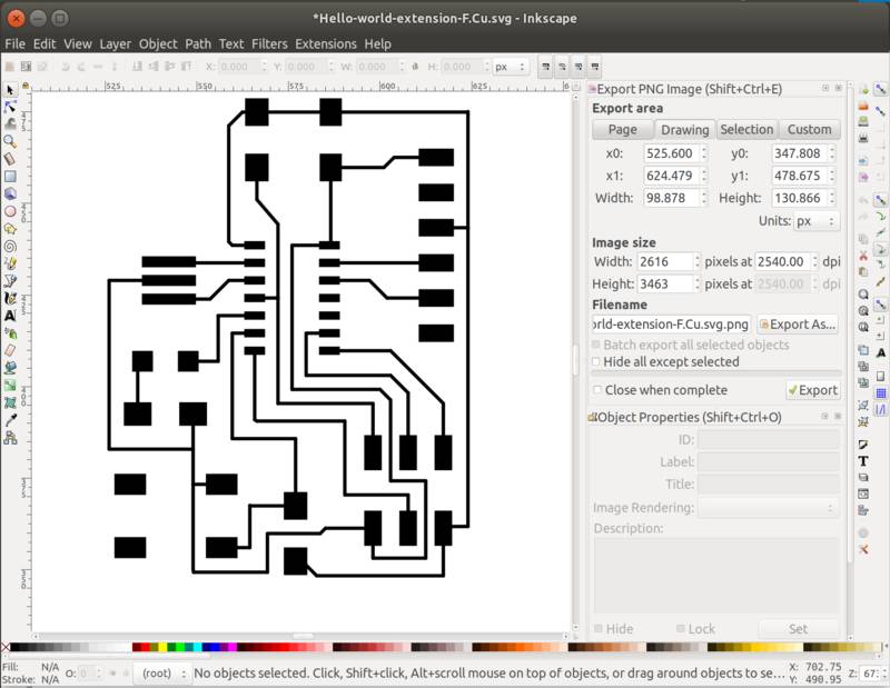
Here is the final schematics for my board:
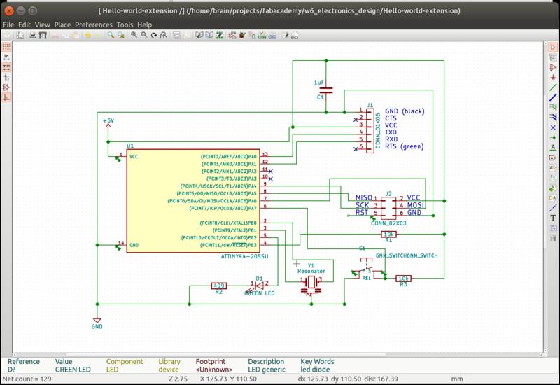
In addition to the Echo hello world board I added a couple of components:
An LED
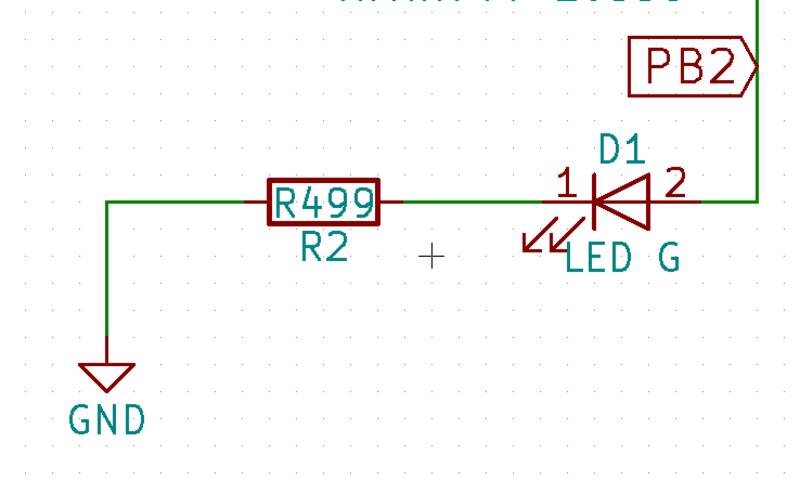
That is combined in series with a R499 resistor to limit the current through the component. We are using the digital output PB2 pin as source current to the LED that on the other side is connected to ground.
There are multiple guides on how to size the LED ( eg. this ) but the idea to use the formula
(Source Voltage - LED Forward Voltage) / Current = Resistancethat is our case gives us(5V - 2.1V) / (10mA / 1000) = 290ohmsA button
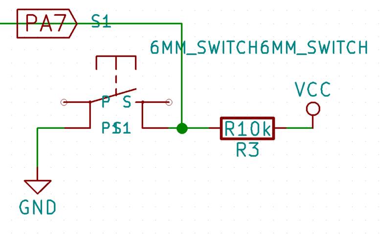
In this design the button is combined with a R10k pull-up resistor and drives the pin PA7.
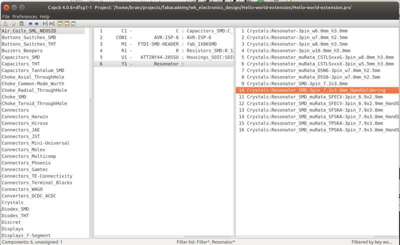
After fixing our schematic we are ready to generate a Net list, and use this in the CVPcb editor to assign a footprint to each component.
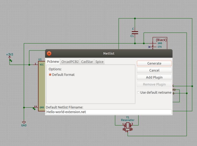
When done we should remember to generate again the Net list from the schematics editor tool so the information about the footprint gets updated.
We are ready now to draw our PCB starting by importing the Net list:
We then try to layout our components a wires on the board until we can find a solution. 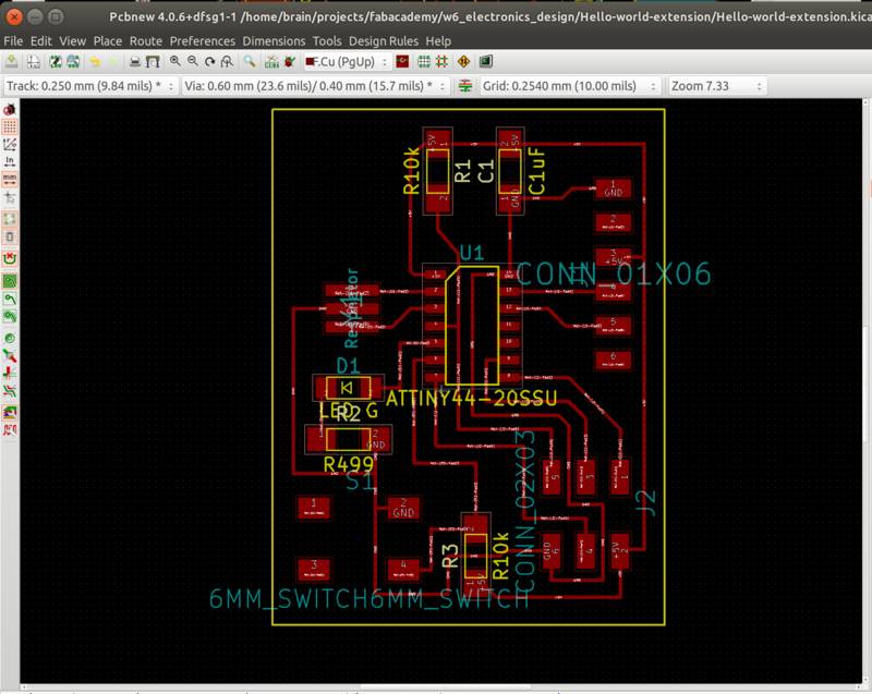
From the design rules menu option we can assign each net to a separate class that has specific rules for track clearance and width.
When done we can run the rule checker to verify if any rule is not met and eventually fix our board.

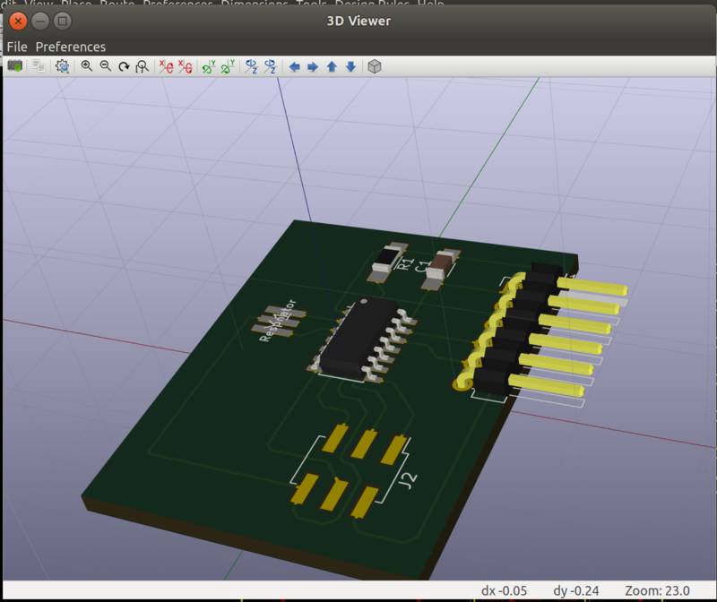
As additional feature KiCAD provides a nice rendering for our board :)
Unfortunately the fablab library doesn’t have a 3D model for all our components.
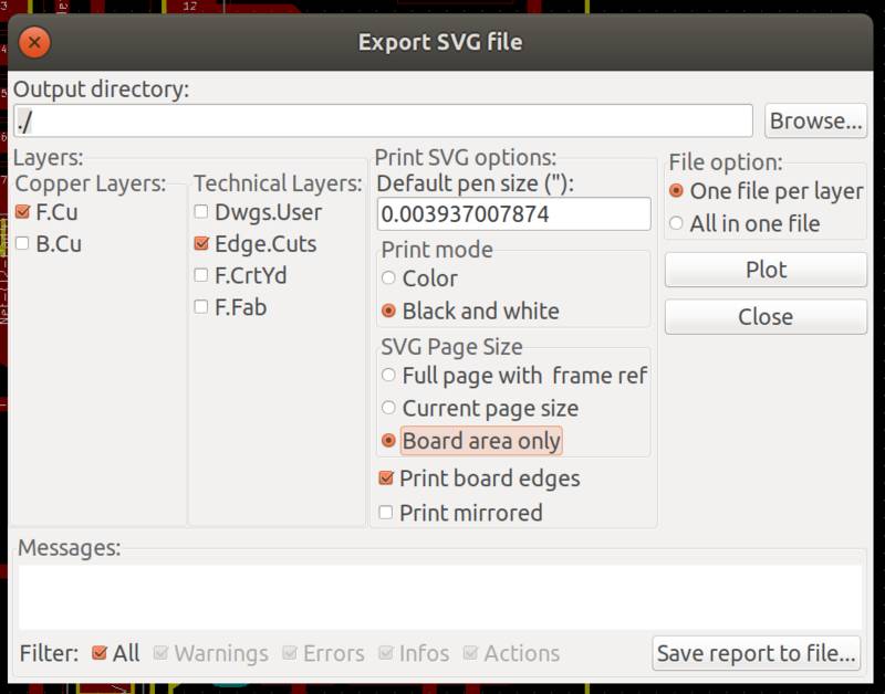
KiCAD has a dedicated layer to draw the outline of our board. It is then very easy to export traces and outline layer separately using the Plot command.
Unfortunately .png file format is not supported. I therefore exported to .svg and then converted them with a image editor to .png making sure we keep a high DPI (>1000) and respect the board dimensions.
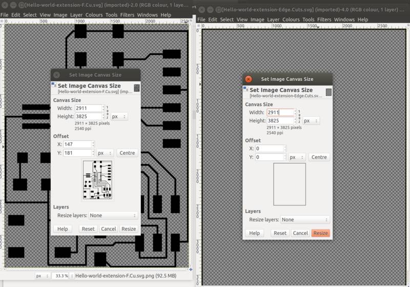
Unfortunately in this process I made a mistake!
According to how mods expect the outline file, we need to invert the B&W colors for that too! :(
Automatic conversion from .svg to .png files
After that mistake I made the conversion described above with imagemagick so that can be easily reproduced and avoid manual mistakes:
convert -density 2540 -units pixelsperinch \
 -colors 2 -negate +dither -type bilevel \
 Hello-world-extension-F.Cu.svg Hello-world-extension-F.Cu.png

convert -density 2540 -units pixelsperinch \
 -fuzz 50% -fill black \
   -floodfill +0+0 white -rotate 90 \
   -floodfill +0+0 white -rotate 90 \
   -floodfill +0+0 white -rotate 90 \
   -floodfill +0+0 white -rotate 90 \
 -colors 2 +dither -type bilevel \
 Hello-world-extension-Edge.Cuts.svg Hello-world-extension-Edge.Cuts.png
Or in a script that converts all the .svg files in a folder detecting the traces/outline by the default KiCAD filenames.
#!/bin/bash

# Converts KiCAD svg export files in .png format for use in fab modules
# see more deatils: http://fab.academany.org/2018/labs/barcelona/students/ilias-bartolini/2018/02/20/week4-electronics-production.html

find . -maxdepth 1 -iname '*-F.Cu.svg' | \
  xargs -L1 -I{} \
    convert \
      -density 2540 -units pixelsperinch \
      -colors 2 -negate +dither -type bilevel \
      "{}" ./"{}".png

TRACES_RESULT=$?

find . -maxdepth 1 -iname '*-Edge.Cuts.svg' | \
  xargs -L1 -I{} \
    convert \
      -density 2540 -units pixelsperinch  \
      -fuzz 50% -fill black \
        -floodfill +0+0 white -rotate 90 \
        -floodfill +0+0 white -rotate 90 \
        -floodfill +0+0 white -rotate 90 \
        -floodfill +0+0 white -rotate 90 \
      -colors 2 +dither -type bilevel \
      "{}" ./"{}".png

CUTS_RESULT=$?

if [ $TRACES_RESULT -eq 0 ]; then
  echo '*-F.Cu.svg converted succesfully'
else
  echo '*-F.Cu.svg not converted'
fi

if [ $CUTS_RESULT -eq 0 ]; then
  echo '*-Edge.Cuts.svg converted succesfully'
else
  echo '*-Edge.Cuts.svg not converted'
fi

if [[ $CUTS_RESULT -eq 0 && $TRACES_RESULT -eq 0 ]]; then
  echo 'Generate your GCode using mods at http://mods.cba.mit.edu/ => Programs => Open server program'
fi
The .rml and .png files are attached, but when trying to mill these I ended up with a board with too small outline because of the problem above.
Download KiCAD Echo Hello project files (.zip kicad project)
Download KiCAD Echo Hello traces and outline files (zipped .rml and .png)
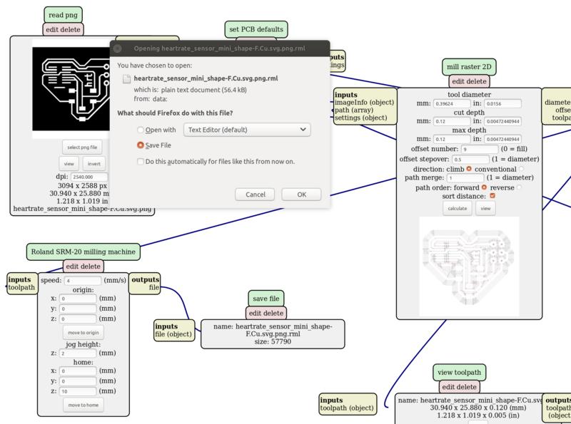
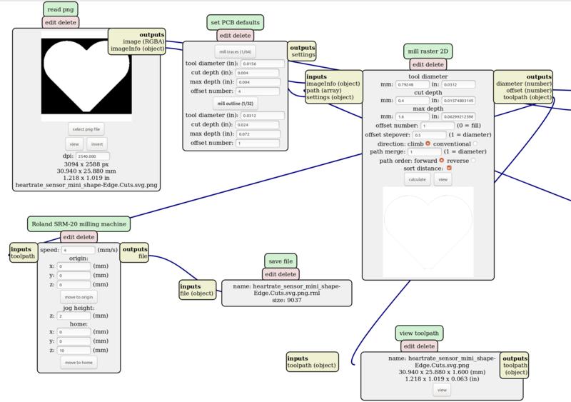
Generating .rml file with mods
During the week4 assignment we have seen how to generate .rml files for the Rolan mill using http://fabmodules.org/.
Because of a bug I started using mods instead of fabmodules since this week. Mods is available at http://mods.cba.mit.edu/ and run on a current version of Niel’s tools. See an in-depth recitation on mods here for details.
The steps are semantically very similar to the one we did on fabmodules.org:
1) Right click => programs => open server program => machins/Roland/mill/SRM-20/PCB
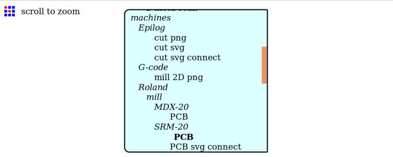
A corresponding mods program is shown in the web page. A program is represented by a graph of modules connected together.
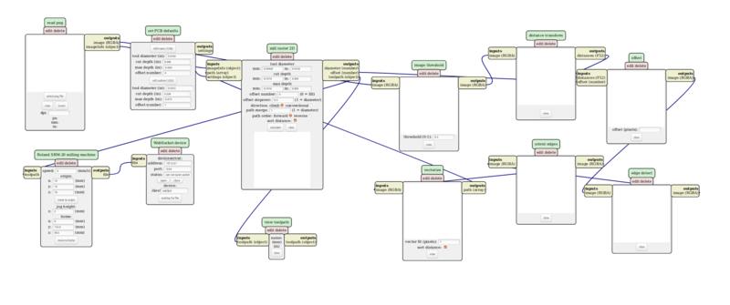
2) In this case we need to replace the final module at the end of the graph “WebSocket device”. Click “delete” on its corresponding link.
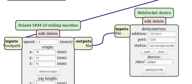
We substitute this with the module that allow us to save a file
Right click => modules => open server module => file/save
By right clicking on the yellow boxes you can link the modules input and outputs. In this case choose “save file / inputs / file” with “Roland SRM-20 milling machine / outputs / file”
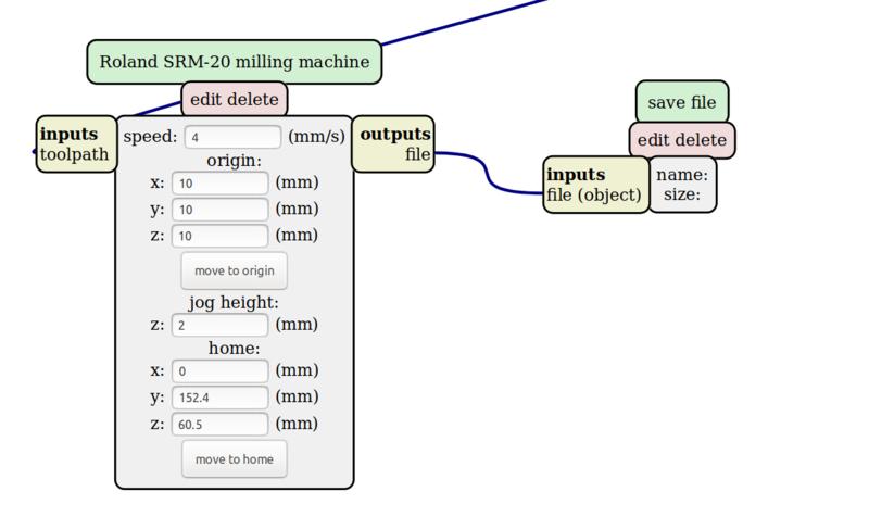
3) Click “select .png file” to upload your traces .png and then click on “mill traces (1/64)” to choose the default settings.
Adjust the following settings for the traces file:
| setting | value |
|---|---|
| cut depth | 0.12mm |
| max depth | 0.12mm |
| origin x | 0mm |
| origin y | 0mm |
| origin z | 0mm |
| home x | 0mm |
| home y | 0mm |
| home z | 10mm |
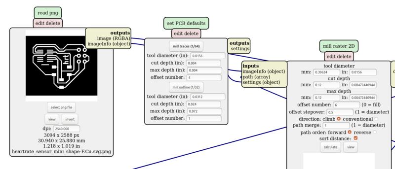
4) Press the “calculate” button and save the .rml file that is prompted.
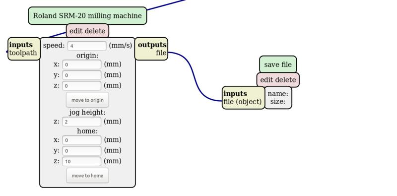
5) Repeat all the step above for the outline / edge file, selecting the “mill outline (1/32)” default settings.
The settings to be adjusted are as above except for:
| setting | value |
|---|---|
| cut depth | 0.4mm |
| max depth | 1.6mm |
| … | … |
Design with Eagle
The process in Eagle is slightly simple and more straightforward:
- Design the schematic
- Create a PCB layout from the schematic
- Export the PCB layout
Additionally Eagle keeps in sync the PCB layout and the schematic we can make changes that are reflected back. In reality I haven’t felt the need or advantage of such a feature.
Similar to KiCAD before starting we need to import the components library for the fablab (Menu Library -> Library manager -> Browse file to add in the Available libraries).
Drawing the schematic is similar to KiCAD. 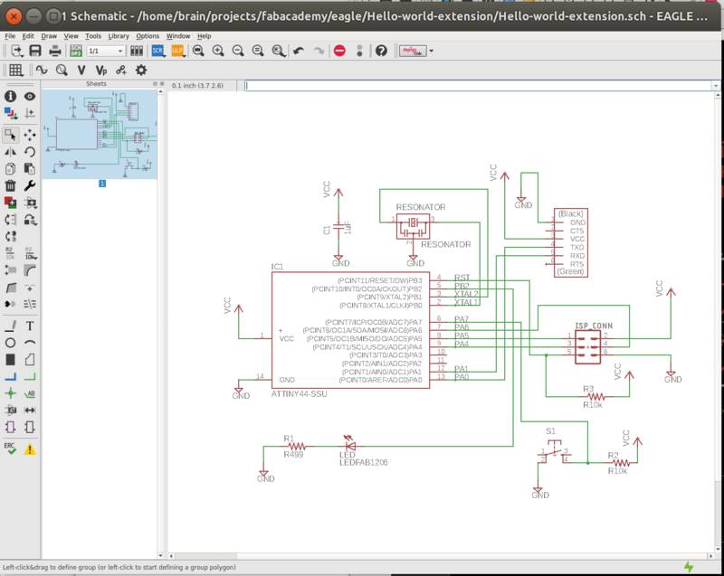
While we update the schematics the components will appear on the PCB layout view. At the end we are ready to place our component and draw the traces.
Here is the final layout:
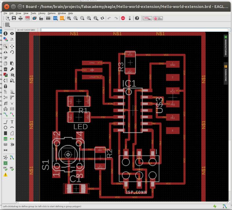
Eagle has as well a rule-checker integrated in Tools -> DRC. There we set the correct wire sizes and clearences to “16mil”.
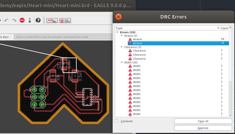
In the image below show some typical errors like Airwire (missing connection/trace), Clearance (traces too close), Width (trace too thin)
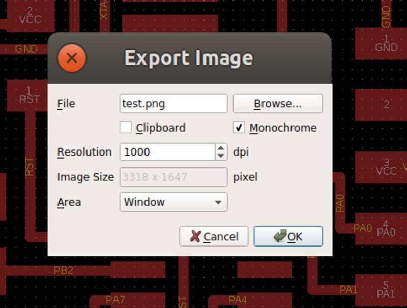
Eagle has native support for exporting B&W .png files. Unfortunately it has no but with an image editor in this case we have to manually separate the outline and traces .png files.
Download Eagle Echo Hello project files (.zip Eagle project)
Download Eagle Echo Hello traces and outline files (zipped .rml and .png)
Board production and test
In the board production I faced some issues:
- see the mistake related to the KiCAD image export above
- error in setting the right origin in mods
The first resulted in a board with wrong outline because of the problem above:
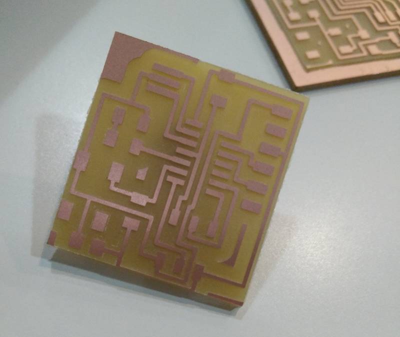
Then I milled it successfully: 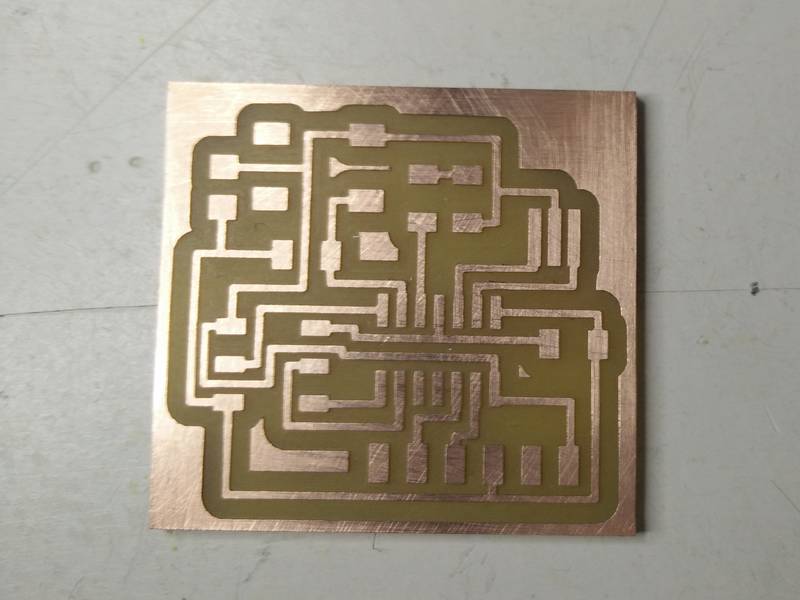
Stuffed the board: 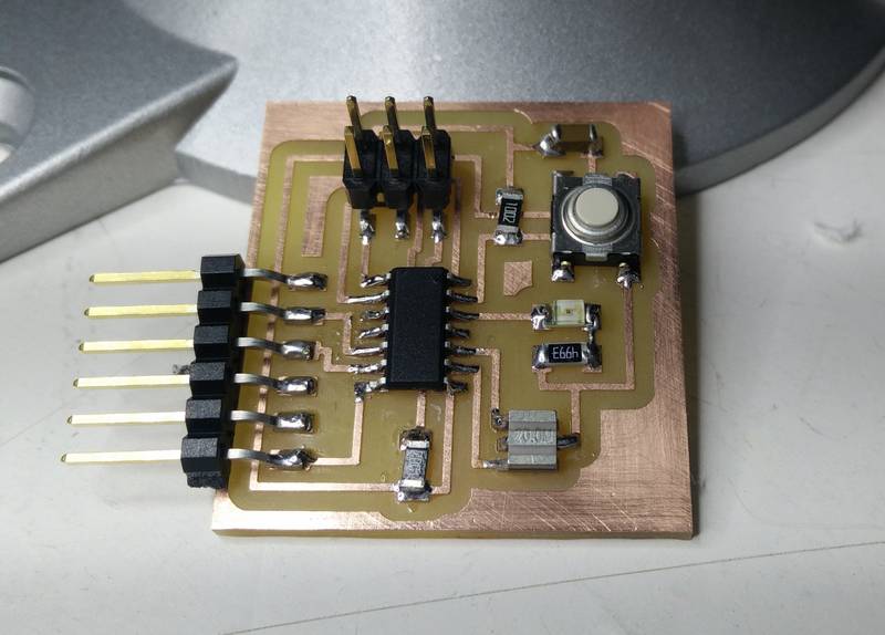
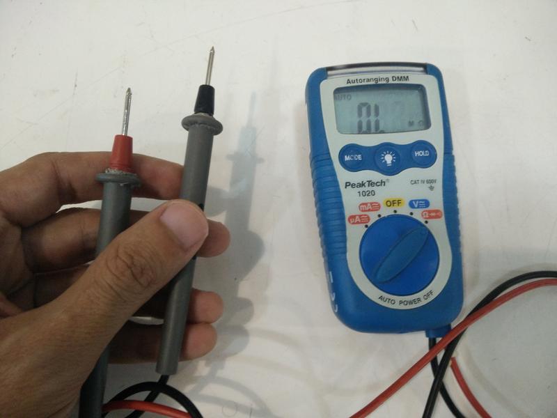
Tested it with a multimemeter the wires connections (we can use the ‘beep’ functionality to detect 0ohm resistance)
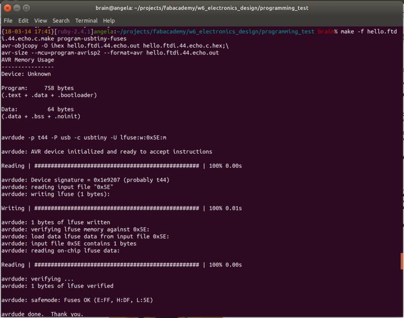
Then we tested the board trying to program it: 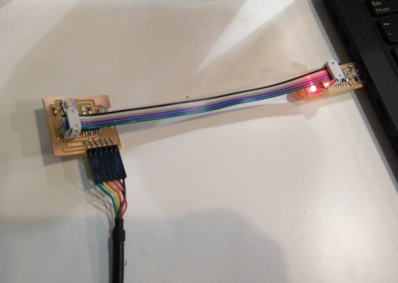
This last step failed with the following error message
avrdude -p t44 -P usb -c usbtiny -U lfuse:w:0x5E:m

avrdude: initialization failed, rc=-1
         Double check connections and try again, or use -F to override
         this check.
and I’m still investigating the cause.
After some times I finally found out that the problem cause was the Tiny44 component mounted in wrong direction ![]()
 …and here finally working!
 ![]()
Full logs available here
Lab test equipment (group assignment)
On top of the multimeter that we used above to check wires:
A multimeter can be used also to measure voltage difference, current and resistance) but it hardly measure signals that are changing quickly with time.
Our lab provides a 2 channels, 150MHz oscilloscope for this purpose:
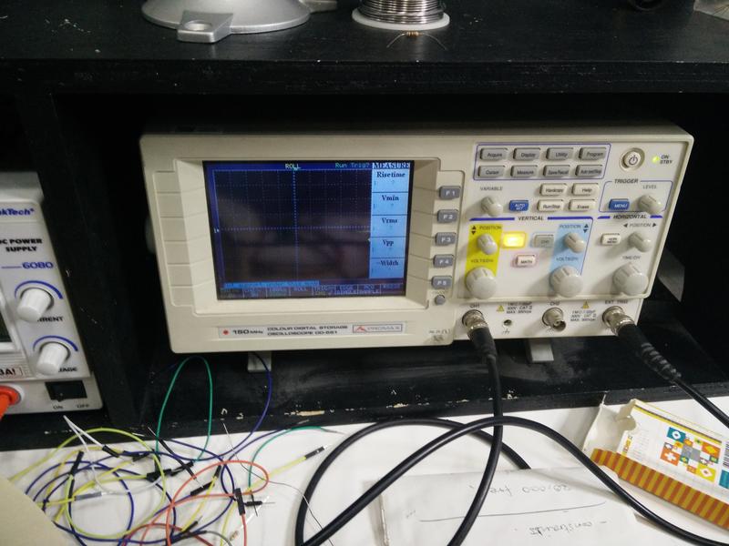
SparkFun aready has a very good guide on How to Use an Oscilloscope that I found useful.
You can see in ‘week 10’ how I used it to test the I2C communication with an accelerometer
Lessons learned
- When drawing the PCB layout I started applying some general strategies. I;m not sure if these are generally good, but they seemed to help me finding a solution:
- Start with placing big components first and then the small ones close to where the related pins are
- Initially ignore the VCC and GND net, start laying our wires that have unique in-out. VCC and GND have in general many placed where they can be connected and have higher degree of freedom.
- When you get stuck start looking at less obvious wires connection options: wires that can go below a component, routing around a pin-wire that is intersecting with your wire.
- If still stuck, disconnect one of the intersecting wires and start searching a different solution.
Finding the right packaging and pins information for each component: refer to the documentation
- For KiCAD
- Export again the Net list after assigning the footprints to each component. Don’t forget! :)
- Select the traces width and set the rules before starting the PCB drawing. 16mil (0.406mm) for traces, 32mil (0.812mm) for the outline lines. Otherwise you’ll have to redraw/update all them basically breaking the layout.
- Could be helpful to try to automate the image conversion progess from .svg. For this reason I created a couple of commands based on Imagemagick. Use
~/bin/fab_convert_pcb_svg_to_png.sh
- Eagle seems to be slightly more user friendly to use and a makes the process slightly simpler. I still made some common mistakes:
- Remember to select the traces width and set the rules to 16mil before starting (32mil for outline) otherwise you’ll have to redraw/update all them basically breaking the layout.
- At the moment of the file generation I didn’t dealise that the “Dimension” layer could be used exactly for the outline and exported separately.
- Check your components orientation… twice!
For the rest of the course I decided to stick to the choice of free software and will keep using KiCAD.
Next steps
- Try a simulation with tools like (ngspice & gspiceui)
- Build a more complex design to learn more design rules
Happy electronics design! ![]()