week 6 - electronics design
-group assignment: use the test equipment in your lab to observe the operation of a microcontroller circuit board
-individual assignment: redraw the echo hello-world board , add (at least) a button and LED (with current-limiting resistor), check the design rules, make it, and test it. extra credit: simulate its operation. extra credit: render it
This week we'll design a Printed Circuit Board (PCB) using an Electronic Design Automation (EDA) software, in this case Autodesk Eagle. This tutorial is very helpful to understand how Eagle works.
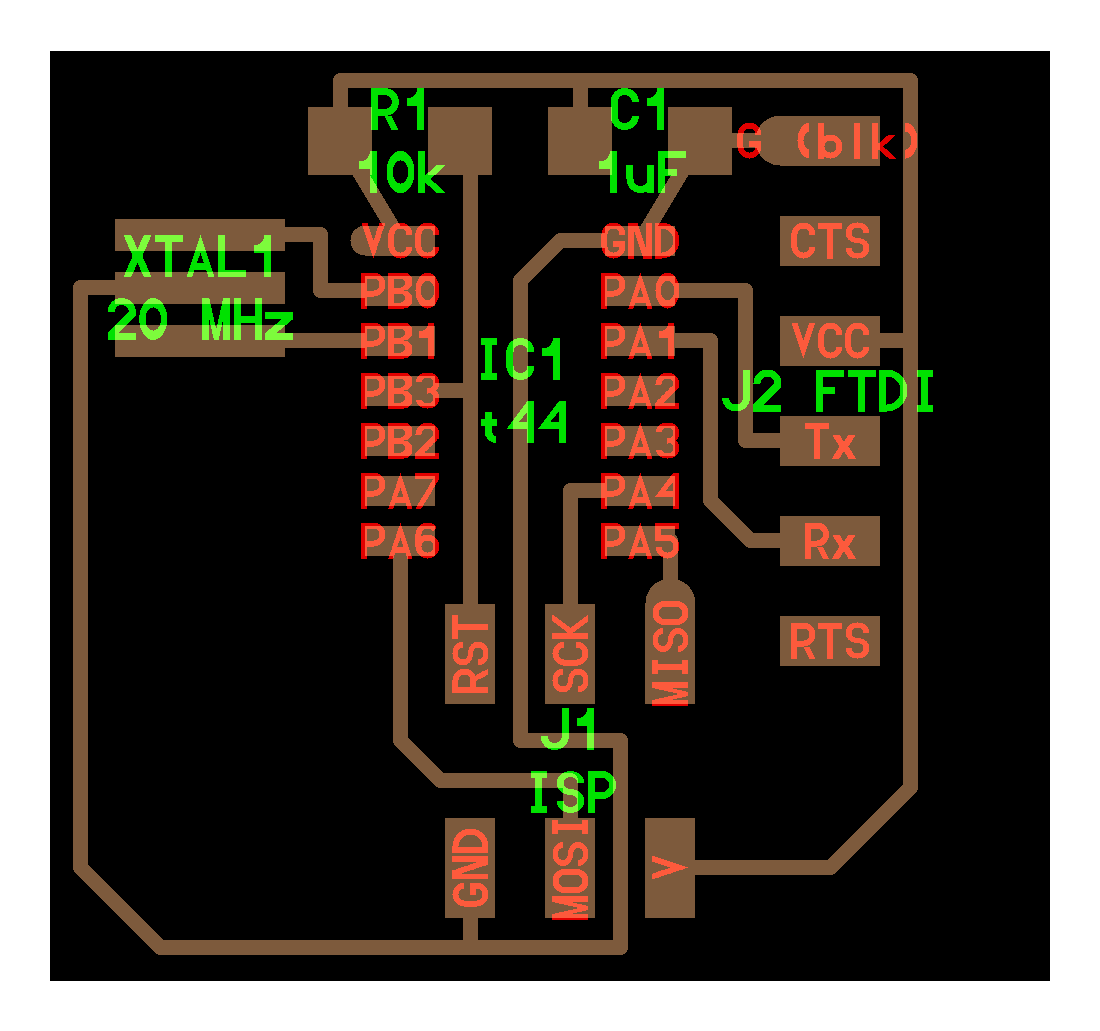
Our starting point is the Echo Hello-World Board:
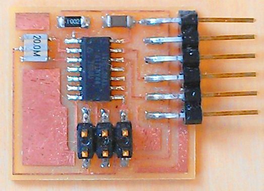
To understand better what components are in it, this picture by Pip summarizes it:
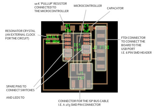
These are the components in it:
-Microcontroller: an ATtiny44 programable chip that controls all the parts on the board and is programmed from the computer.
Pull-up resistor: this 10K resistor keeps the power flowing into the microcontroller steady near VCC or zero (This needs to be connected to the VCC pin on the ATtiny)
-Capacitor: this device stores electric charge. It consists of one or more pairs of conductors separated by an insulator. This will help filter devices to remove voltage or signal spikes in our circuit.
-FTDI Connector: Connects the circuit to the computer to read in the program and power the board (Its VCC and GND pins need to be connected to the respective VCC and GND circuits on the board, and it's Tx and Rx pins connect to the two free pins on the microcontroller.)
-SMD Bus Connector: Takes in information from the FabISP and connects it to certain pins on the Microcontroller to program the board. (This needs to be connected to VCC and GND on the respective pins on the Microcontroller, and the other pins need to be connected to free input and output pins)
-Resonance crystal: This is an external clock for the circuit (It needs the input traces to be connected to two pins on the board and the ground trace to the GND circuit)
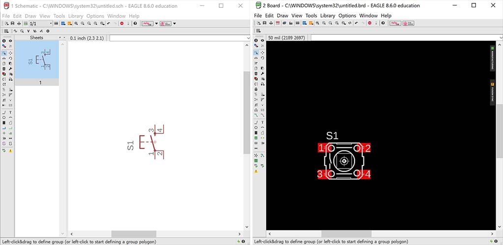
So this is basically the Echo Hello-World Board. However, we will add a Button and a LED (with current-limiting resistor) to it. To do this we will use the spare pins, which are the free pins on the microcontroller.
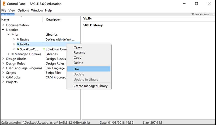
To design our board, we will use Eagle. First we will need to import the FabLab Components Library fab.lbr Download the file and place it into the library folder "EAGLE 8.6.0/lbr". Then launch Eagle and activate the library by going to 'libraries', find the fab.lbr and click on 'use'.
Then go to File>New and create a New Schematic (sch). Also create a New Board (brd), when asked 'Create from schematic?' say Yes.
- A schematic in electronics is a drawing representing a circuit. With the use of symbols, it represents electronic components. The lines represent the conductors or traces. When the wires are connected in a diagram, a dot is shown at their intersection.
- The board layout shows how the electrical componets and traces will be laid out on the board.
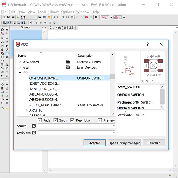
In the schematics, to add components, use the add button on the left toolbar, which pops up the library window. Here are all the components are listed alphabetically, so under the fab library you can find all the components for your board:
· 2 x RES-US1206FAB
· 1 x 500k RES-US1206FAB
· 1 x ATTINY44-SSU
· 1 x 6 pin header AVRISPSMD
· 1 x 1 uF CAP-US1206FAB
· 1 x LED 1206
· 1 x 6 pin header FTDI-SMD-HEADER
· 1 x 20 MHz RESONATOR
Once you add a component in the schematic it will also appear in the board layout.
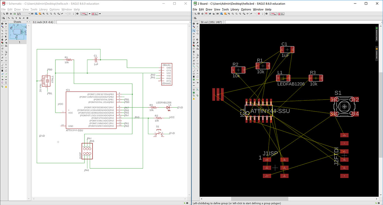
Add the rest of components in the schematic and connect them using the tool Net on the left toolbar. You can draw direct lines from one connection/pin to another connection/pin. A second way of connecting things is drawing just a small path from one connection, name it and label it (right clic on the path>Name/Label), and draw another small path from another connection and also name it and label it the same way. By doing it this second way, a pathless connection will automatically be created from one connection to the other. You can also mix both ways of doing.
There's one last step before you can check off on your schematic design, checking for connectivity with an Electrical Rule Check (ERC).
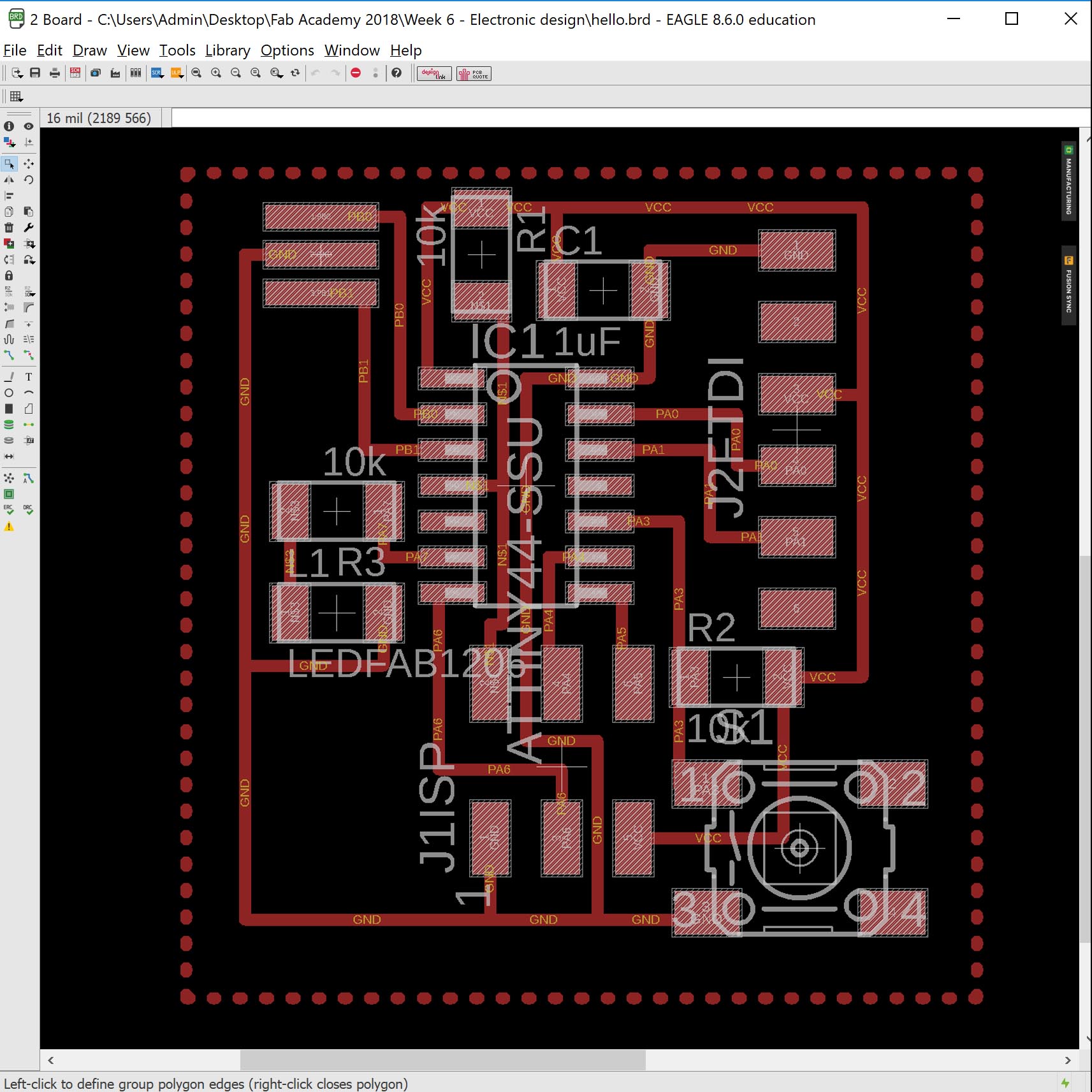
Once you are done, move onto your Board layout and you will see all the connections you did in the schematics are represented in the board layout as yellow lines.
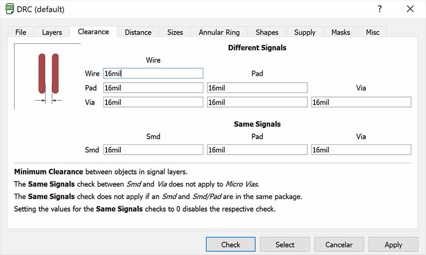
First thing, set up the clearance values in DRC (Design Rule Check). Clearance is the distance between two elements. This one can't be smaller than the drill-bit size of the milling machine. In our case is 16mil (1⁄64 inch). You can also set up the grid to the size of the clearance so that its easier to move around components when distributing them on the board.
You can re-arrange the components by dragging them (click on the '+' sign on each component). You can rotate them by right-clicking on them while they are dragged. Place them so the connections are closer. Once they are aligned as you want, use the Route tool to draw the connecting traces. Set up the width value of the routes to 16mil.
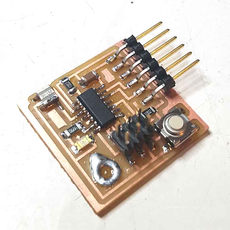
With some patience, I ended up with this layout:
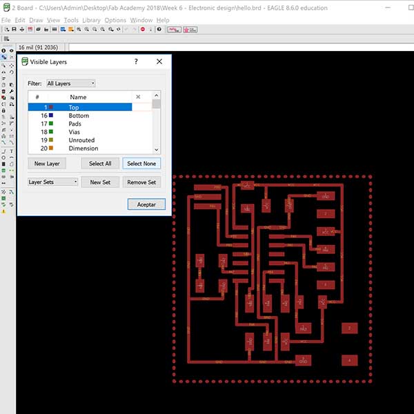
To export the layout, we have to hide all layers (information, names...) except for the red one with paths.
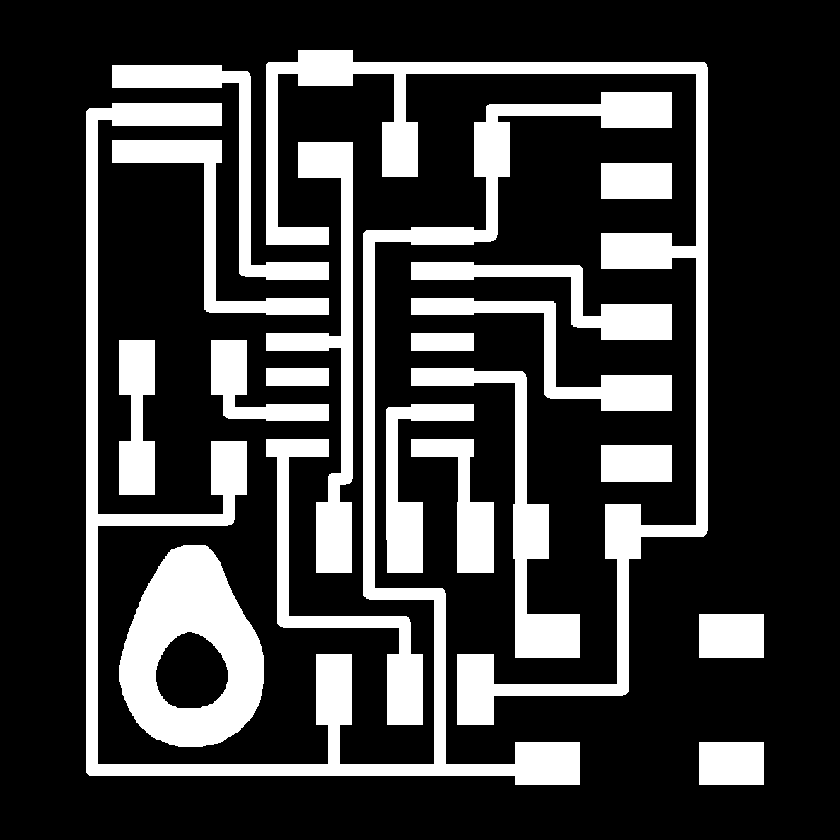
Then go to File>Export>Image, mark 'Monochrome' and choose a resolution bigger than 500dpi. The picture on the left is the resulted Traces image I exported (I added a personal touch in Photoshop). The one on the right is the Outline image, you will need to draw this one yourself keeping in mind that the cutout line should be at least as thick as the tool (1/32=0.793mm) so a 8mm thick outline should be ok.
The following steps are pretty much the same as in the electronics production week. With the png's we generate the milling strategy in mods to get the gcode for the milling machine.

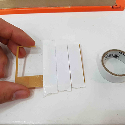
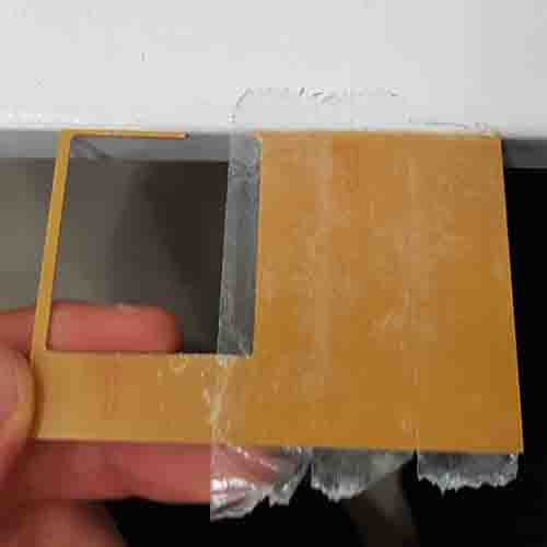
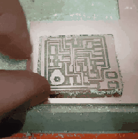
Then tape the pcb to the wood block on the plate of the Roland SRM-20.
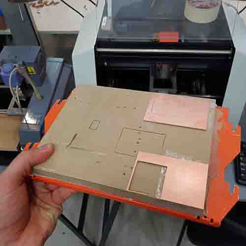
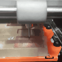
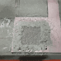
Place the milling bit, set the origin, load the gcode on the Roland and proceed with the milling
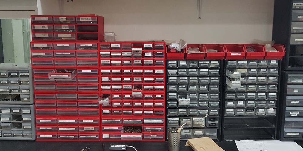
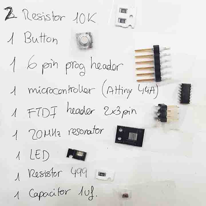
Then prepare all the components for soldering.
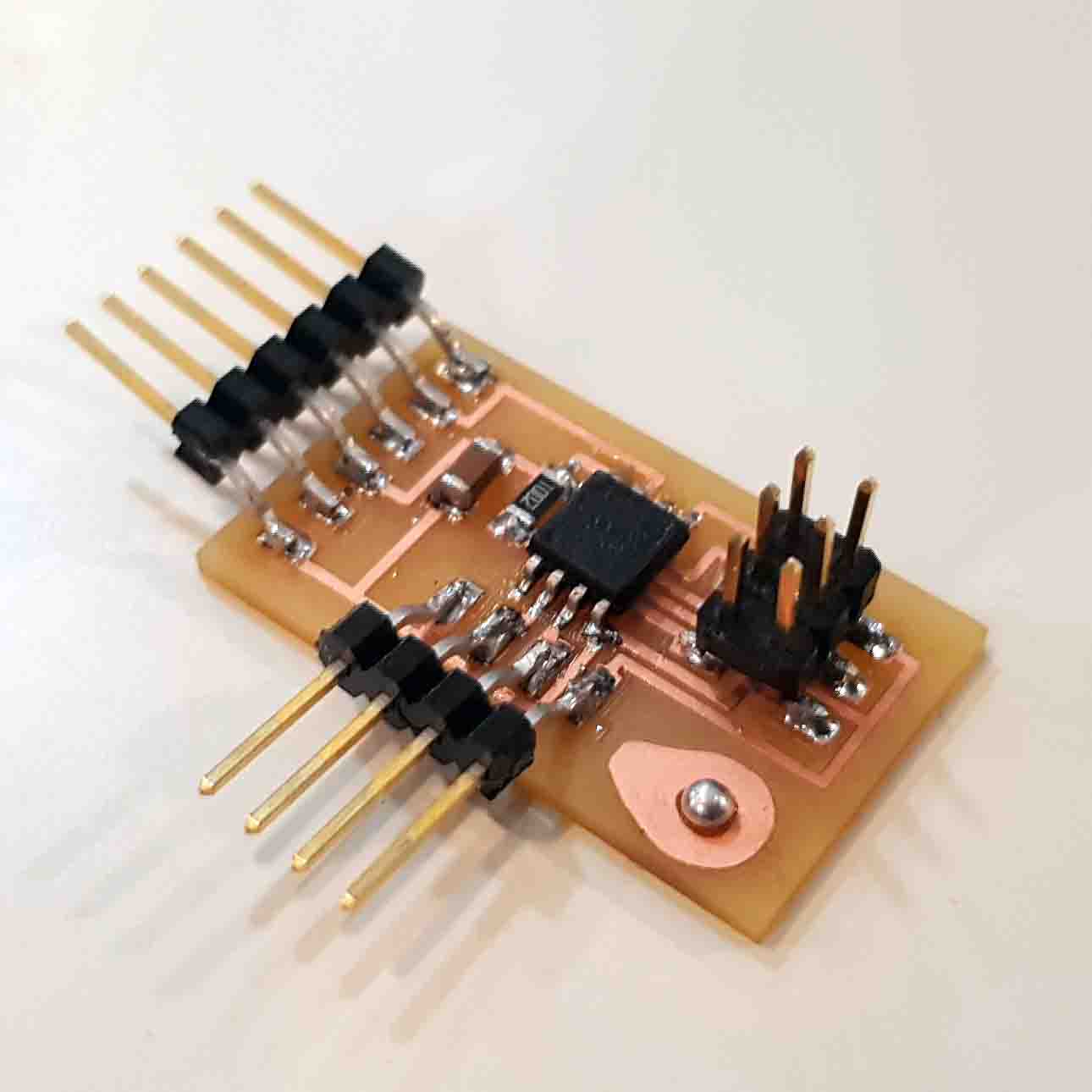
And solder everything on the milled pcb. (btw, not a big deal but I made a mistake in my avocado: I wanted to put solder on the seed, not the meat, but solder will never stick to the pcb phenolic resin layer. I fixed this in the board for the output devices week)
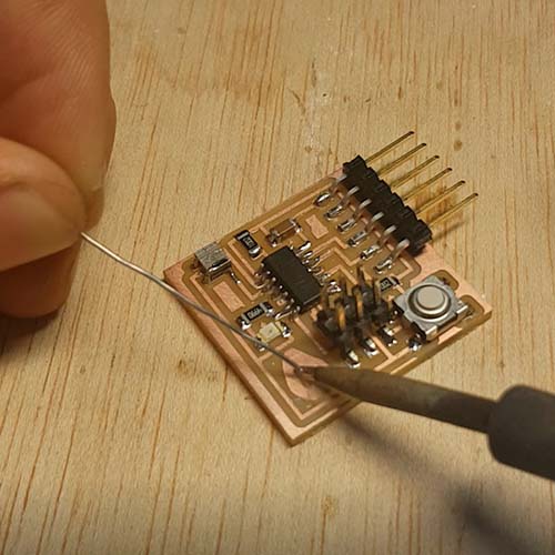
Before programming, the digital multimeter (DMM) is useful for checking that all our connections are working and detecting possible bad connections. Turn the multimeter into the Continity Test Mode. With the circuit de-energized, place the test leads across the component being tested. It will beep if a complete path (continuity) is detected. If the circuit is open the DMM will not beep, therefore we will know there is a bad connection between one multimeter lead and the other.
download files

This work is licensed under a Creative Commons Attribution-NonCommercial-ShareAlike 4.0 International License.