Embedded Programming Master Class
Embedded programming Master Class with guillem and victor
Intro
ATtiny 44 & 45
the first number “4” is the memory 4k ()
the second number is the familly
in the AVR familly
tiny familly arduino use the mega familly
why the software to compile are open source
questions about chip : octopart
ATTINY44A-SSU A-SSU is for the packaging (basicaly the shape) DIP (through hole components) is the shape you use on breadboard
throug holes component are becoming harder to find, that is why we use smd components
the chip has pins 1 for VCC 1 for Ground pins (4) have extra fonctionality on top (MISO, MOSI, RST, .. for ISP) but we can use them to other purposes

the chip does not know PIN3, arduino abstract this for us

Install boards in Arduino Follow these instructions
select Attiny24/44/84 change programmer USBTinyISP
be carefull of the pin number arduino and chip ones are differents
blink a led using arduino
open blink exemple
change pin number
Send it to the board
blink a link using C
What arduino bring

The blue blocks are from arduino
AVR GCC toolchain : avr-gcc + avr-ar + avr -objcopy + avrdude
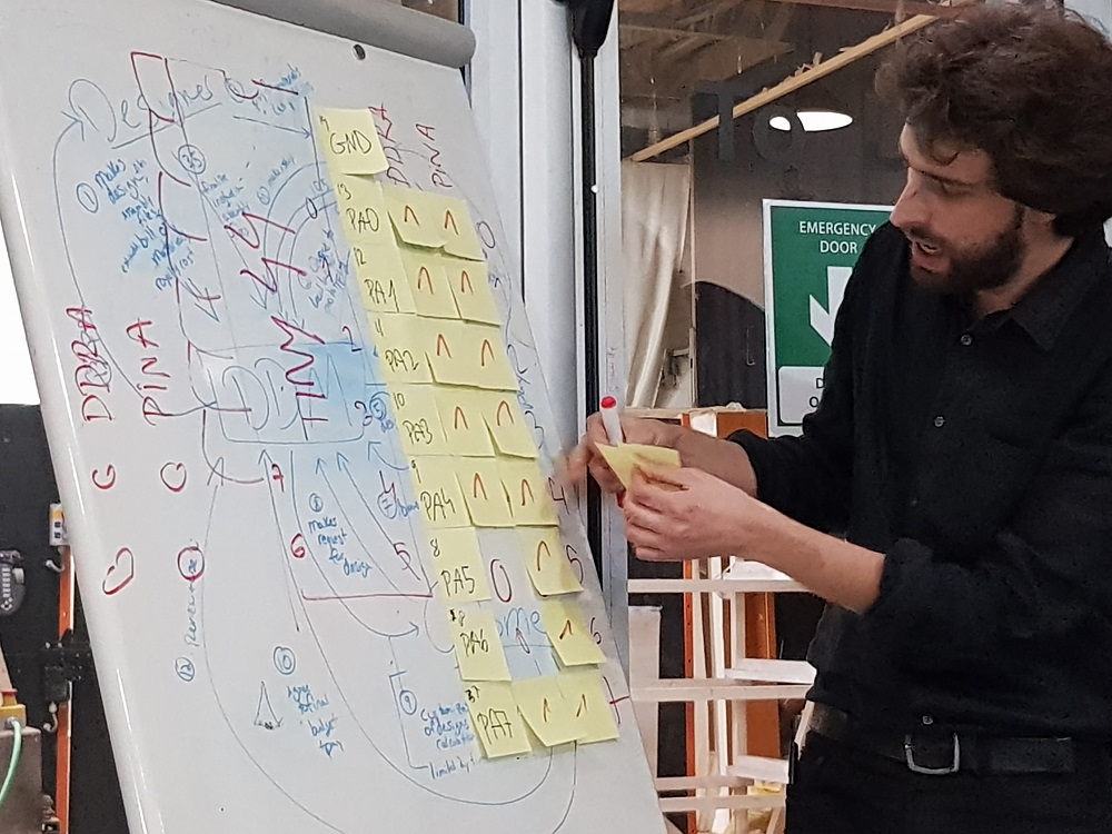
read the datadheet to knwo how the chip works the memory is very important its a big array of switches
the first row (registers) change the state of the pins
memory switch have address from 0 to … go to register summary
a row hav 8 switches (0 yo 7), a row hav an address 0x
rows: PORTA DDRA PINA are used to control our pins
here we want to use PA7 (pin 6 on chip)
1 Bit is 0 or 1 8 bits is 1 Byte 10110101
DDRx register is used to tell if pin is an input or an output (data direction register) PORTx (port x data register) read data from pin PINx (port x input register) write data
to write into memory we need to write all row
DDR : 1 is output
| Bit | 7 | 6 | 5 | 4 | 3 | 2 | 1 | 0 | |
| DDRA | 1 | 0 | 0 | 0 | 0 | 0 | 0 | 0 |
DDRA (var from avr/io.h) 0b prefiw is used to tell it’s a byte
so DDRA will be set to 0b10000000 (for 0b 1000000) to turn pin 7, actually #7 of the chip, as an output
DDR is a marco for the memory address 0x1A
same for PORTA to write on pins 0 to 7
Blink exemple in C
`#include <avr/io.h> #include <util/delay.h>
int main(void) { DDRA = 0b10000000;
while (1) {
  PORTA = 0b01000000;
  _delay_ms(1000);

  PORTA = 0b00000000;
  _delay_ms(1000);
}
}`
Bit shifting `1«1 = 0b00000001 1«2 = 0b00000010 1«3 = 0b00000100 …
1«6 = 0b01000000`
Bit masking
PORTA = 0b00000000;
OR operation:
0b01000000 <= (1<<6)
0b00000000 <= PORTA
--------------------
0b01000000 <= PORTA
PORTA = 0b01000000;
| PORTA = (1 « 6) | PORTA |
Macros ‘#define pinOutput(port, pin) ((1 « pin) | port)
call :
pinOutput(DDRA, 6)
is equivalent as
| PORTA = (1 « 6) | PORTA; |
how arduino works
`#include <avr/io.h> #include <util/delay.h>
int main(void) { setup();
while (1) {
  loop();
}
}`
Build chain
GCC-AVR to compile AVRDUDE to upload

ISP
Fuses : There are 3 bytes of permanent storage in the chip called fuse low byte, fuse high byte and fuse extended byte
Makefile
Make run commands in Makefile without argument it compile
we have to run twice
make
make us
avr-gcc -mmcu=attiny44 -Wall -Os -DF_CPU=1000000000 -I./ -o hello.button.44.out
attiny44 1Mhz for internal clock
Stay in touch
Hi, I'm
Joris Navarro, from Perpignan (France), a proud dad, a fab director/manager, a teacher, a ceo, a FabAcademy student, but not only. Click here to know more about me.
Check my work for FabAcademy on FabCloud GitLab
@joris.navarro.
Want to say Hi ? Please send me a message.