From Welding To Soldering.
For this week’s group assginment - visit here.
I’m a mechanical engineer, always with a big welding gun in my hand but it was time to play witht he little one, The soldering Iron.
Thing I did this week :
- Learned to use FabModules and The Milling Machine - SRM-20
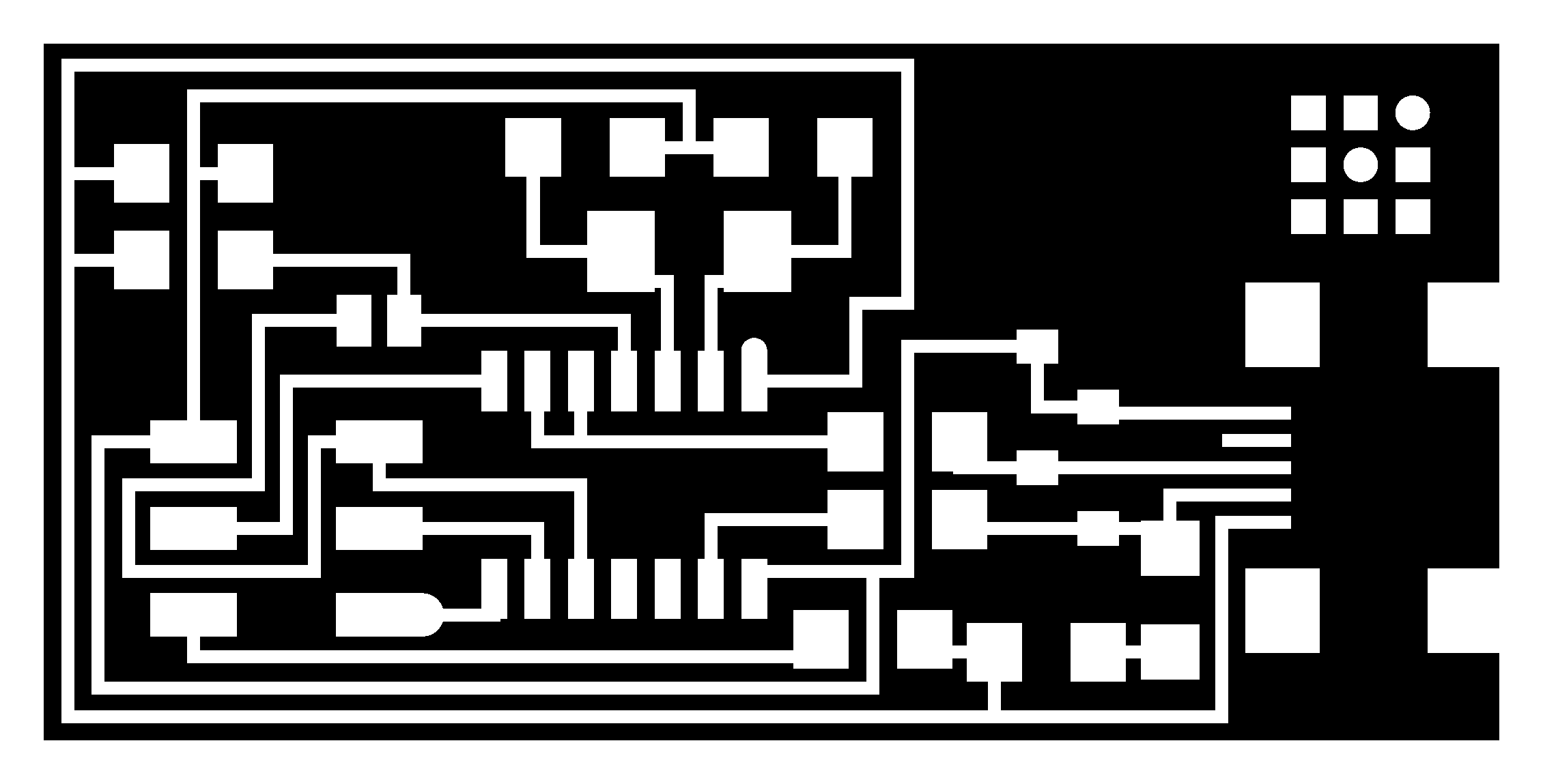
- Milled a PCB
- Learned abot different Components
- Soldered the components to the PCB
- Fell Sick
First Thing first
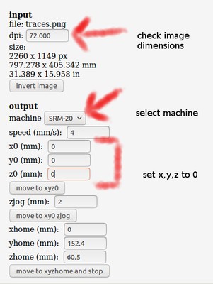
Our Lab Incstructor started with teaching us how to use the FabModules, we started with importing the .png file ,secelting the output format and then the process we wnated to do. Then he went on and told us about the different parameter our machine uses to mill te perfet PCBs.
Step-1
- Goto to Fab Modules and seelect the input image type.
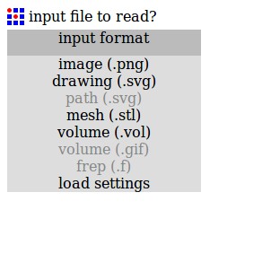
I chose this ISP to mill :
Step-2
Next Select the output image type. In my cas it was .rml or Roland Mill since we have a Roland SRM-20 at the lab.
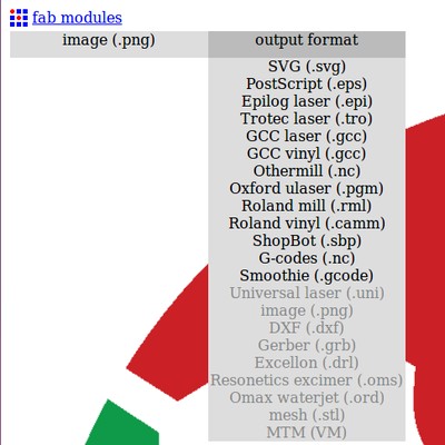
Step-3
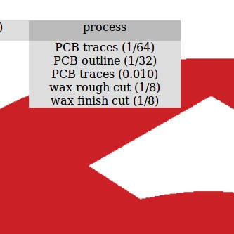
Now select the process : 1. Traces to cut the path, 2. To Cut the board outline to prey it out.
Step-4
Now on the right hand side check whetehr the dimensions of the image are correct and then select th Machine.
Step-5
- Let’s look at all the different parameters we can set for our machine to mill the perfect PCB.
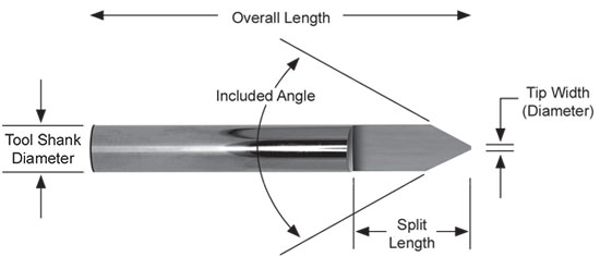
- Before moving forward i would like to tell you that we used V-BIT to mill our traces. In a V-Bit tool, the tool dimater of a v-bit will increase with the increase in Cut Depth.
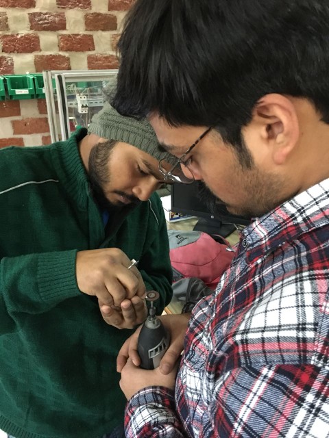
Our Bit was pretty worn out and the tip was broken too, me and Rahul tried to mend it my grinding the tip of the tool witht he help of a dremel. After a bit of effort out Makeshift V-bit was ready to use. Hale Rahul Gauatam.
Now Let us look at the different parameters :
1. Cut Depth
Cut depth is pretty self explanatory, it is how deep you want the tool to cut in your PCB. Generally the cut depth shpuld be equal to the thckness of the COpper Film on the PCB.
I used 0.12 as it worked best for out makeshift V-bit.
2. Tool Diameter
Tool Dimater is the diamter if the tip of the tool, For tracing we use 1⁄64 and to cut the outer edge we use 1⁄32. Since in our lab we use a V-bit instead of the 1⁄64 bit, thorugh some trial and error TOOL DIAMTER of 0.35mm works best for us,
3. Number of offsets
To learn what Number of offset means, let us assume that we are doing a pocket milling operation(we mill out a pocket). In the image the toolpath is denoted by Red Lines. Now the number of red lines is the number of offsets, in the image the offset is 4, if for instance the offset was 2, the tool would only cover the first 2 paths.
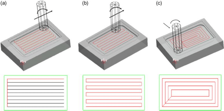
4. Offset Overlap
Our tool Diamter is 0.35, now lets assume it mills the blue line first, the next which is to be milled is the Red one, Optimally the difference b/w the redd and blue line should be equka to the tool diamter which is 0.35mm. But to be on the safer side we give a certain overla percentage so that the cuttng head goes over the preiously cut path and makes sure there is no residue left.
*Blue and Red lines are the tool path.
 Here we can see the overlap of the tool.
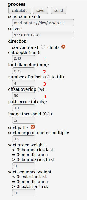
After Setting all the parameters, hit Calculate and then save the file
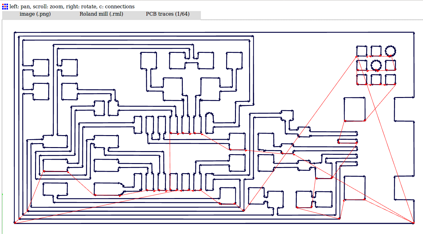 * This is final file FabModules Produce.
Let us make PCB’s
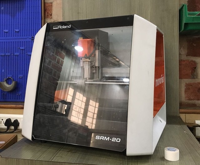
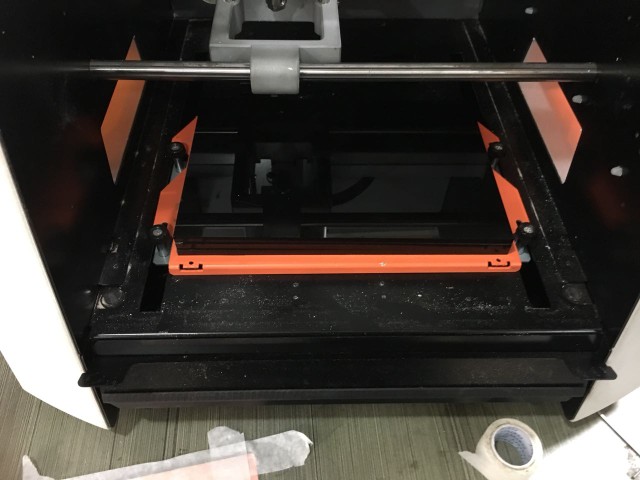
- Machine Used :
Modification Done to the bed of the machine :
- Earlier there was a wooden sacrificial layer attached to the bed, they also helped to raise the height of the platform.
- Problem - We use Double Sided tape to attach the PCB to the wood, but it does’t adhere to it well. To rectify the problem I lasered cut some acrylic pieces to make the new bed base and sacrificial layer.
- OLD Base:
- NEW Base:
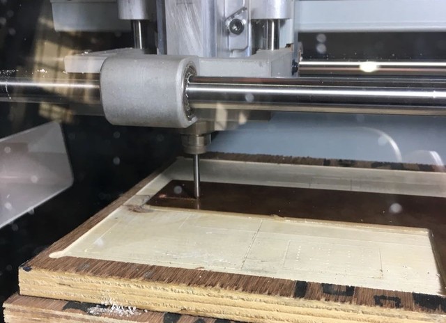
- After mounting the Acrylic Base, I milled the entire surface to make it parallel with the tool.
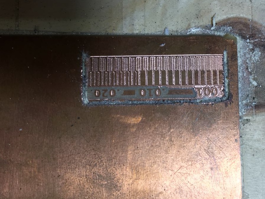
- The next step was to print the LINE TEST to test the machining capibilty SRM-20.
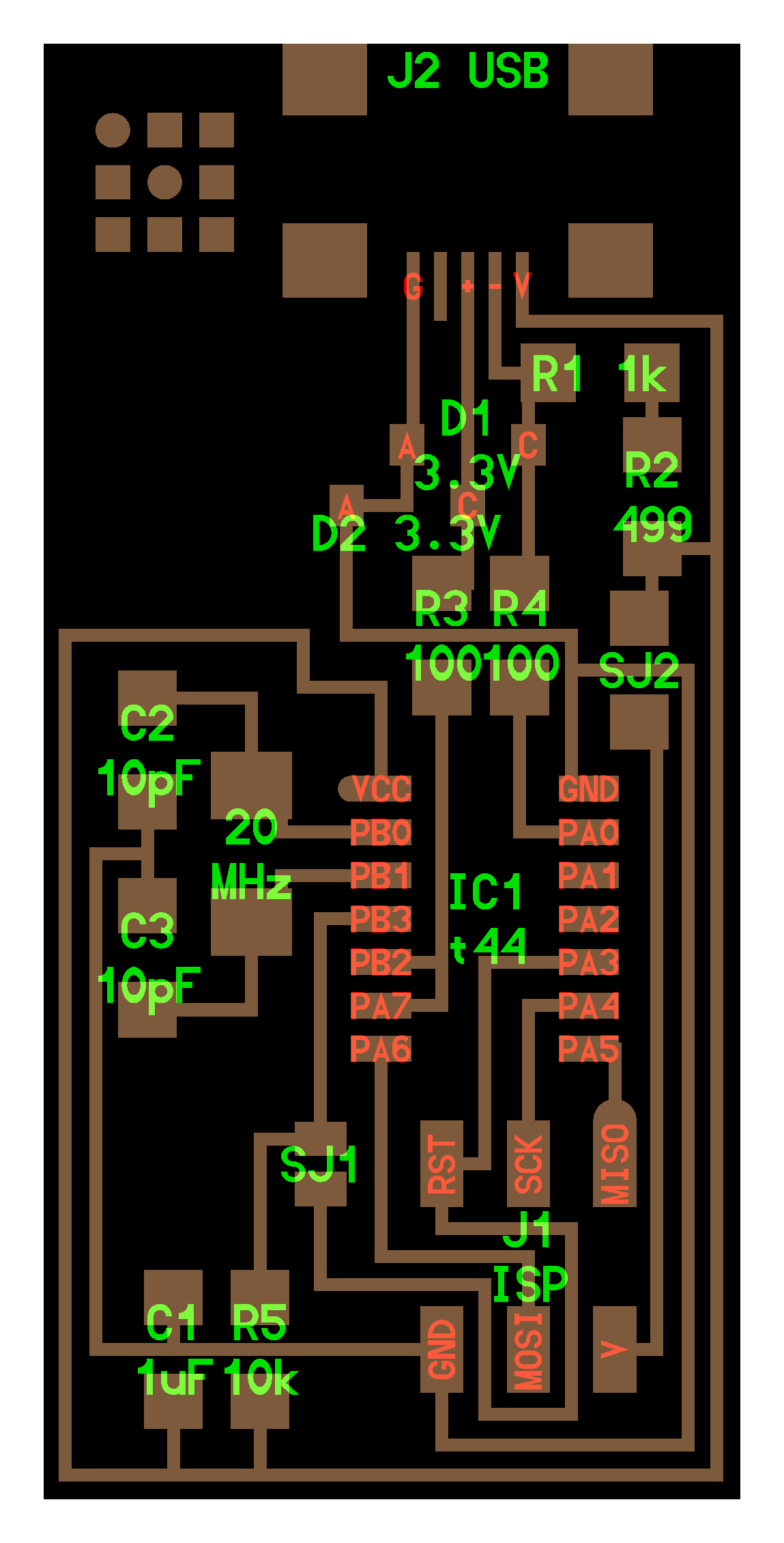
FABISP
- After the test it was time to mill out the FABISP and collect the component to be mounted.
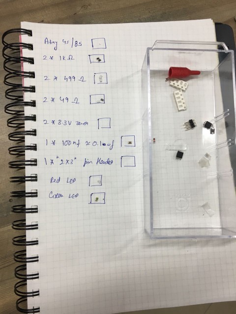
Before moving on, Me and my Fablab instructor sorted all the compnents and placed them in the drawers systemtaticaly.
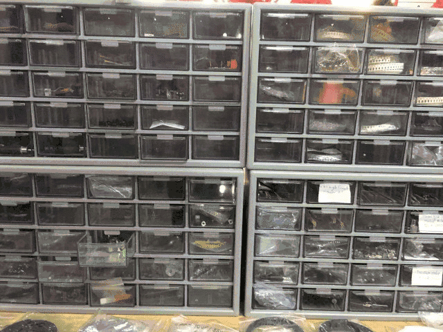
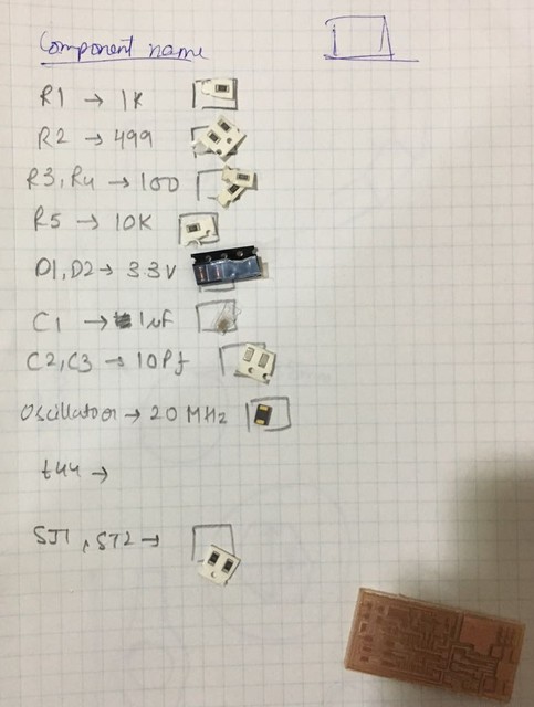
- Components listed and arranged :
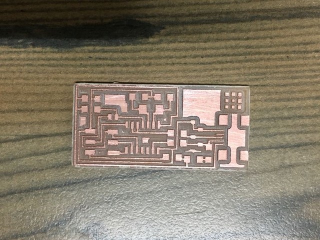
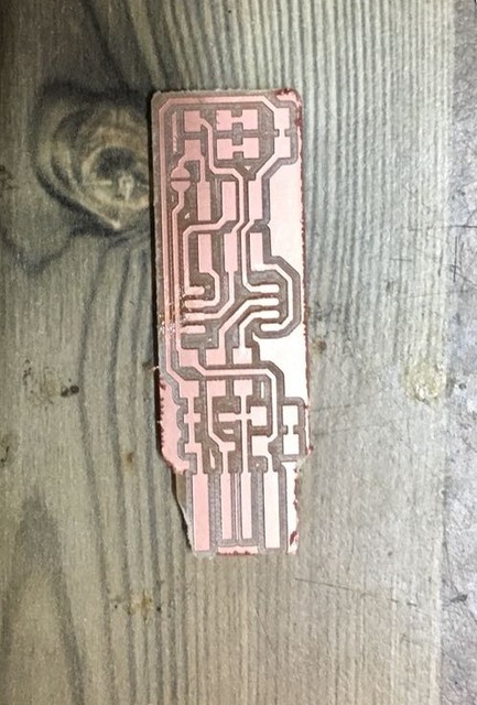
Milled Circuit :
Components Mounted on to the FabISP :
As you can see i did’t mount the USB mini B, since i knew that the whole board was a mess and its not gonna work whatsoever.
Brian’s ISP
Other students at the lab were making the Brian’s ISP, to i decided to do the same since it can connect to the computer directly.After couple of failed attempts a not so perfect but doable board was milled and i started working on it.
Components listed and arranged :
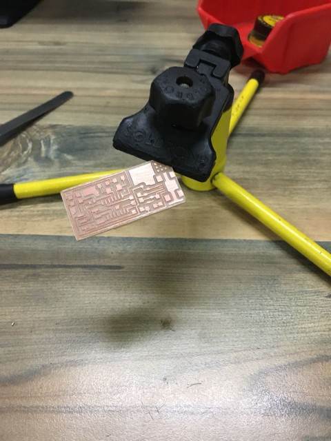
Milled Circuit :
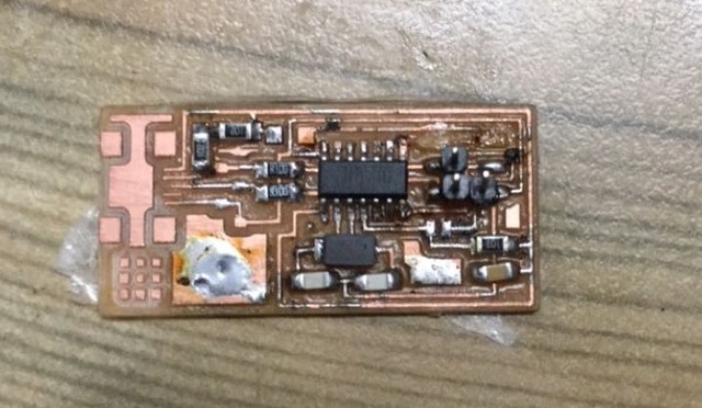
Components Mounted on to the FabISP :
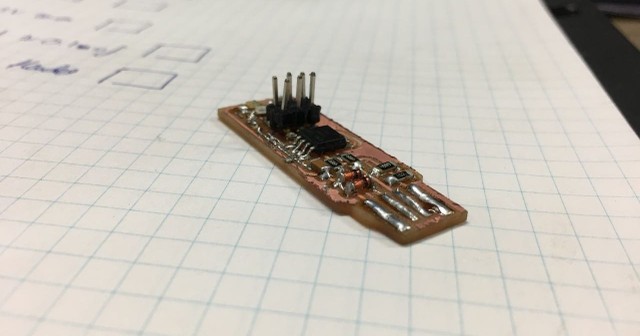
After mounting all the components i plugged it into the USB port of my laptpop and Both the Red and Green LED’s lit up, without caring about it much i decided to programme by following Brian’s Documnetation. And obviously Failed, beforee programming the ISP I again checked all the connections with a multimemter and found 2 problems, 2 out of 6 legs of ATtiny45 were not attached to the PCB. I fixed all the three prblems and tried again. This time it went super smooth and in no time i had a programmed ISP in hand.
Programming :
To program the ISP, I repeated the steps Explained in Brian’s documentaion.
Software Installation
In the Terminal :
For Ubuntu and other Debian-based distributions, enter the following command, followed by your password when prompted: ~~~~ sudo apt install avrdude gcc-avr avr-libc make ~~~
- Get and Build the Firmware
Download the firmware source code and extract the zip file (on Linux, unzip fts_firmware_bdm_v1.zip). Open your terminal program and cd into the source code directory.
Run make
This will build the hex file that will get programmed onto the ATtiny45. When the command completes, you should now have a file called fts_firmware.hex.
- Program the ATtiny45
-Programmer used - AVR ISP MK 2.
- Edit the file called Makefile.
Near the top of the file, find
PROGRAMMER ?= usbtiny
and change usbtiny to avrisp2.
If you installed correctly the red LED lights up.
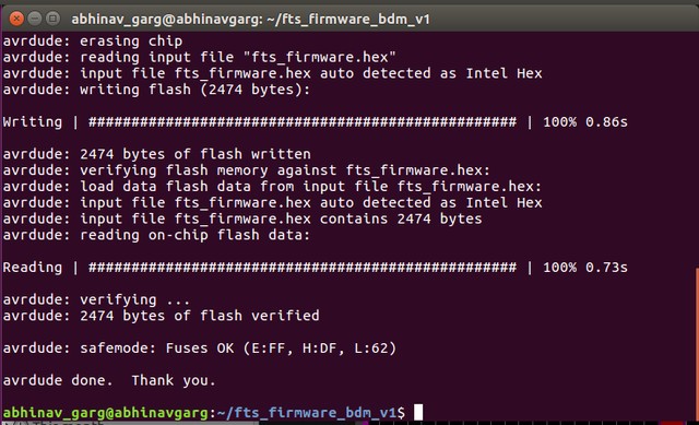
Connect the programmer to the ISP header on your board. Run make flash. This will erase the target chip, and program its flash memory with the contents of the .hex file you built before.
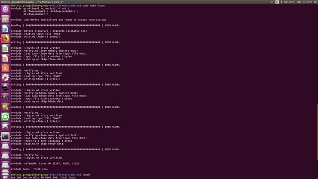
Once you’ve succesfully programmed the flash memory, it’s time to set the configuration fuses. We’ll do this in stages: First, set the fuses that control where the microcontroller gets its clock source from. Run the make fuses command. This will set up all of the fuses except the one that disables the reset pin.
Test the USB Functionality
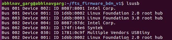
Unplug your board from the USB port and disconnect the programmer, then plug it back in to the USB. Make sure the programmer you used to program your board is also disconnected from the computer.
Type lsusb in the terminal, which will list USB devices. If you see a “Multiple Vendors USBtiny” device, it worked!
Sceenshots :
Bye !!