Week 14
Getting started with Networking & Communication
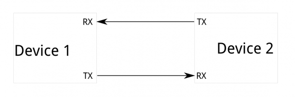
This weeeks assignment was to create a network either wired or wireless which would be able to communicate 2 Microcontrollers.......
For this week I decided to work on I2C protocol...... well ... I didn't know much about this protocol but I know that using this protocol about 128 Microcontrollers can be connected together ..... each node is having its own address and the master of the netwrok can access any node using this address ...... to have a better understanding of the I2C Protocol with ATTINY I followed This Link
Through this link a very good image of the protocol can be made ........ and after going through this link I was able to understand how I2C works ...... But apart from understanding the protocol ...... Now it was the turn to realize this protocol ...... I was comfortable with Arduino IDE .... So I was a bit confused how to realize this ....... how to transmit standard data packets for the protocol ..... etc etc ....... but after surfing through internet pages ..... the image of I2C using arduino became more clear and I got to know it was quiet easy to use with Arduino IDE Using Wire.h Library ....... every node can be identified by an address which we can designate ...... and through this address master can communicate to any of the node .......
Overview Of I2C Protocol
The Inter-integrated Circuit (I2C) Protocol is a protocol intended to allow multiple “slave” digital integrated circuits (“chips”) to communicate with one or more “master” chips. Like the Serial Peripheral Interface (SPI), it is only intended for short distance communications within a single device. Like Asynchronous Serial Interfaces (such as RS-232 or UARTs), it only requires two signal wires to exchange information.
Why Use I2C? What’s Wrong with Serial Ports?
Because serial ports are asynchronous (no clock data is transmitted), devices using them must agree ahead of time on a data rate. The two devices must also have clocks that are close to the same rate, and will remain so–excessive differences between clock rates on either end will cause garbled data.
Asynchronous serial ports require hardware overhead–the UART at either end is relatively complex and difficult to accurately implement in software if necessary. At least one start and stop bit is a part of each frame of data, meaning that 10 bits of transmission time are required for each 8 bits of data sent, which eats into the data rate.
Another core fault in asynchronous serial ports is that they are inherently suited to communications between two, and only two, devices. While it is possible to connect multiple devices to a single serial port, bus contention (where two devices attempt to drive the same line at the same time) is always an issue and must be dealt with carefully to prevent damage to the devices in question, usually through external hardware.
Finally, data rate is an issue. While there is no theoretical limit to asynchronous serial communications, most UART devices only support a certain set of fixed baud rates, and the highest of these is usually around 230400 bits per second.
What’s Wrong with SPI?
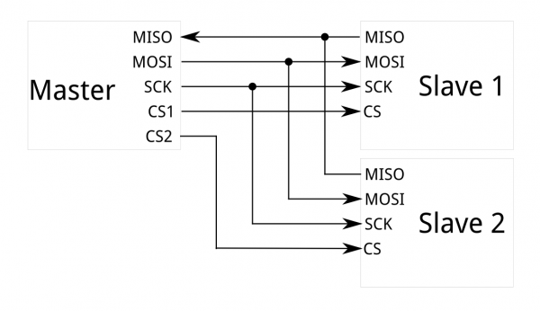
The most obvious drawback of SPI is the number of pins required. Connecting a single master to a single slave with an SPI bus requires four lines; each additional slave requires one additional chip select I/O pin on the master. The rapid proliferation of pin connections makes it undesirable in situations where lots of devices must be slaved to one master. Also, the large number of connections for each device can make routing signals more difficult in tight PCB layout situations. SPI only allows one master on the bus, but it does support an arbitrary number of slaves (subject only to the drive capability of the devices connected to the bus and the number of chip select pins available).
SPI is good for high data rate full-duplex (simultaneous sending and receiving of data) connections, supporting clock rates upwards of 10MHz (and thus, 10 million bits per second) for some devices, and the speed scales nicely. The hardware at either end is usually a very simple shift register, allowing easy implementation in software.
Enter I2C - The Best of Both Worlds!
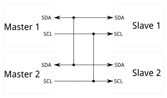
I2C requires a mere two wires, like asynchronous serial, but those two wires can support up to 1008 slave devices. Also, unlike SPI, I2C can support a multi-master system, allowing more than one master to communicate with all devices on the bus (although the master devices can’t talk to each other over the bus and must take turns using the bus lines).
Data rates fall between asynchronous serial and SPI; most I2C devices can communicate at 100kHz or 400kHz. There is some overhead with I2C; for every 8 bits of data to be sent, one extra bit of meta data (the “ACK/NACK” bit, which we’ll discuss later) must be transmitted.
The hardware required to implement I2C is more complex than SPI, but less than asynchronous serial. It can be fairly trivially implemented in software.
Protocol
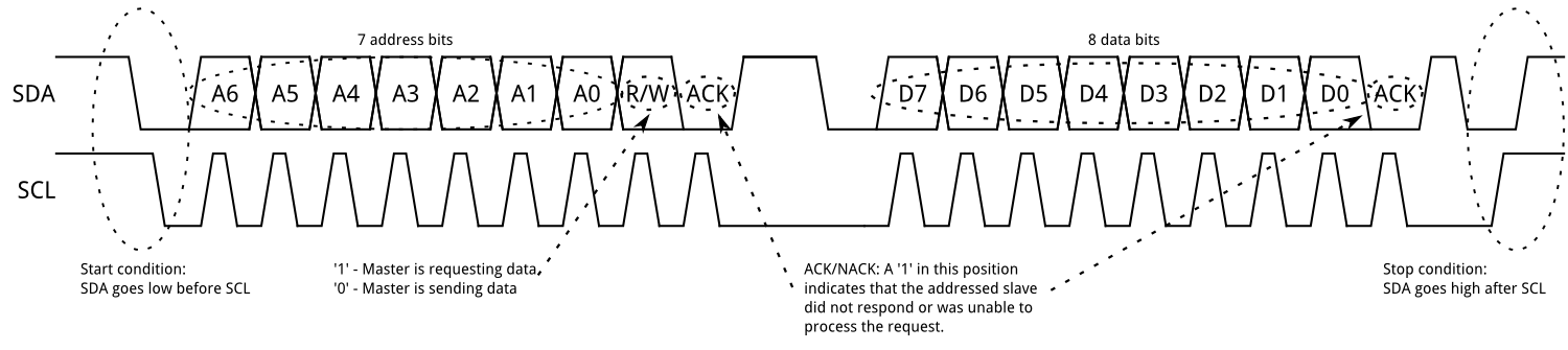
Messages are broken up into two types of frame: an address frame, where the master indicates the slave to which the message is being sent, and one or more data frames, which are 8-bit data messages passed from master to slave or vice versa. Data is placed on the SDA line after SCL goes low, and is sampled after the SCL line goes high. The time between clock edge and data read/write is defined by the devices on the bus and will vary from chip to chip.
Start Condition
To initiate the address frame, the master device leaves SCL high and pulls SDA low. This puts all slave devices on notice that a transmission is about to start. If two master devices wish to take ownership of the bus at one time, whichever device pulls SDA low first wins the race and gains control of the bus. It is possible to issue repeated starts, initiating a new communication sequence without relinquishing control of the bus to other masters; we’ll talk about that later.
Address Frame
The address frame is always first in any new communication sequence. For a 7-bit address, the address is clocked out most significant bit (MSB) first, followed by a R/W bit indicating whether this is a read (1) or write (0) operation.
The 9th bit of the frame is the NACK/ACK bit. This is the case for all frames (data or address). Once the first 8 bits of the frame are sent, the receiving device is given control over SDA. If the receiving device does not pull the SDA line low before the 9th clock pulse, it can be inferred that the receiving device either did not receive the data or did not know how to parse the message. In that case, the exchange halts, and it’s up to the master of the system to decide how to proceed.
Data Frames
After the address frame has been sent, data can begin being transmitted. The master will simply continue generating clock pulses at a regular interval, and the data will be placed on SDA by either the master or the slave, depending on whether the R/W bit indicated a read or write operation. The number of data frames is arbitrary, and most slave devices will auto-increment the internal register, meaning that subsequent reads or writes will come from the next register in line.
Stop condition
Once all the data frames have been sent, the master will generate a stop condition. Stop conditions are defined by a 0->1 (low to high) transition on SDA after a 0->1 transition on SCL, with SCL remaining high. During normal data writing operation, the value on SDA should not change when SCL is high, to avoid false stop conditions.
Now that we understand about I2C we need to go through the pin Diagram of the ATTINY 44 to identify SDA and SCL pins, These pins would be used for I2C Communication.
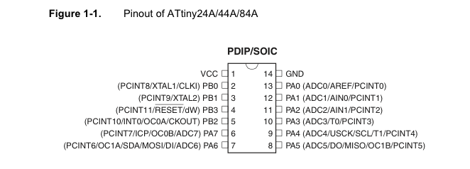
From the diagram it may be noticed that PA6 and PA4 are the SDA (Serial Data) and SCL (Serial Clock), these pins would be furthur considered while designing the PCB.
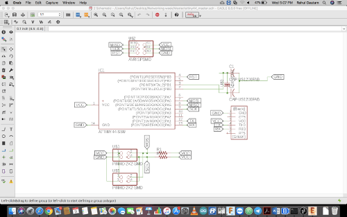
Now that the I was able to understand I2C protocol and confident to code the controllers...... I started with making the board files for the master and slave ....... I went through Labs inventory first to check the availability of the components and then moved furthur to make PCB on Eagle.......
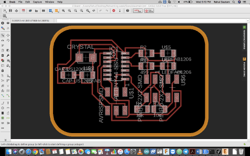
The below one is for the master
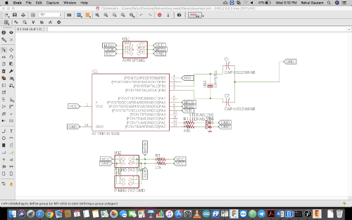
This one is for the slave
Milling and Soldering
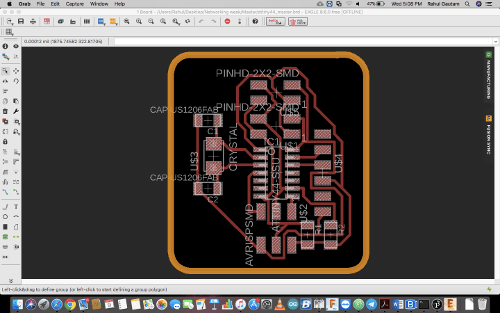
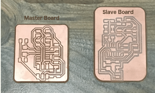
Now since my design was ready ........ The designs were ready to mill .... and after milling ....
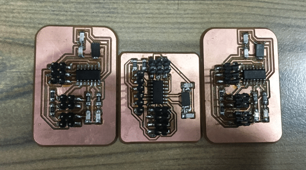
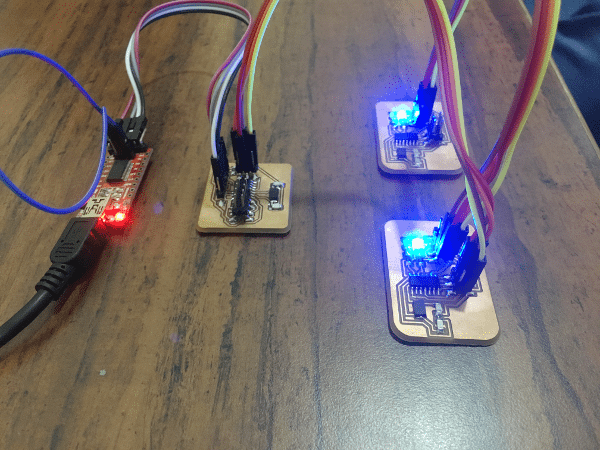
Now after milling the boards I soldered all the components on the board ....... and here is the Hero Shot of the same .....
I made 2 slave boards and 1 Master Board .......
Connections
Now for making a network we need to connect all the boards together...... for connections this is a schematic, how to connect the slave boards to master.
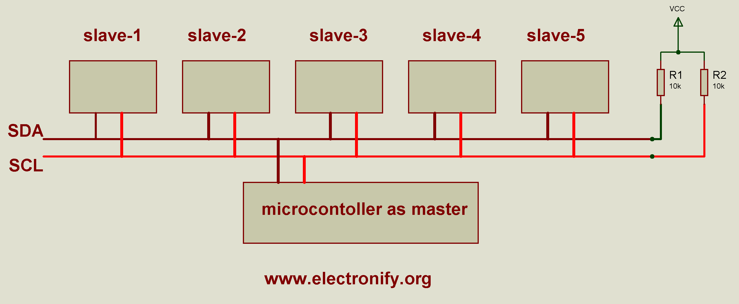
Pic Courtesy : www.electronify.com
Actual Connections
Programming
Master Code
#include "Wire.h" // This is I2C library
#include "SoftwareSerial.h" // This is used for making rx tx pins using software
#define Rx 0
#define Tx 1
SoftwareSerial myserial(Rx, Tx); // declared Rx and Tx Pins

void setup() {
  Wire.begin(); // I2C communication Started
  myserial.begin(9600); // Serial communiation Started
  myserial.println("Communication Started");
}

void loop() {
  char d; // Character type declaration to store a character.
  if (myserial.available() > 0)
  {
    d = myserial.read(); // Read serial and store its value in variable d.
    if (d == '1') {   // Now transmit data over the I2C lines according to the cases.
      Wire.beginTransmission(1); // Communication started with first node
      Wire.write(1); // Value sent over the channel
      Wire.endTransmission(); // Communication Ended
      myserial.println("send :- ");
      myserial.print(d); // Print on Serial Monitor

    }
    if (d == '2') {             // Same of others.
      Wire.beginTransmission(1);
      Wire.write(2);
      Wire.endTransmission();
      myserial.println("send :- ");
      myserial.print(d);

    }
    if (d == '3') {
      Wire.beginTransmission(2);
      Wire.write(3);
      Wire.endTransmission();
      myserial.println("send :- ");
      myserial.print(d);

    }
    if (d == '4') {
      Wire.beginTransmission(2);
      Wire.write(4);
      Wire.endTransmission();
      myserial.println("send :- ");
      myserial.print(d);

    }

  }
  delay(10); // Delay to make sure whole CPU is not consumed.
}
Note: To understand the code read comments
Slave Code 1
#include "Wire.h" // This is I2C library

int led1 = A0;
int led2 = A1;

void setup() {
  Wire.begin(1); // I2C Communication Started
  Wire.onReceive(receiveEvent); // Event triggering i.e this event will be called only when some data is recieved

  pinMode(led1,OUTPUT); // Declared the nature of the pin OUTPUT LED 1 Connected
  pinMode(led2,OUTPUT); // Decalerd the nature of the pin OUTPUT LED 2 Connected
}

void loop() {
  delay(100);
}


void receiveEvent(int howMany) {
  int x = Wire.read(); // Read Data over the channel
  if (x == 1)
  {
    digitalWrite(led1,HIGH); // if 1 is recieved Make LED1 pin HIGH
    digitalWrite(led2,LOW); // if 1 is recieved Make LED2 pin LOW
  }
  if(x ==2)
  {
    digitalWrite(led1,LOW); // if 2 is recieved Make LED1 pin Low
    digitalWrite(led2,HIGH); // if 2 is recieved Make LED 2 pin HIGH
  }

}
Note: To understand the code read comments
Slave Code 2
#include "Wire.h"

int led1 = A0;
int led2 = A1;

void setup() {
  Wire.begin(2);
  Wire.onReceive(receiveEvent);

  pinMode(led1,OUTPUT);
  pinMode(led2,OUTPUT);
}

void loop() {
  delay(100);
}


void receiveEvent(int howMany) {
  int x = Wire.read();
  if (x == 3)
  {
    digitalWrite(led1,HIGH);
    digitalWrite(led2,LOW);
  }
  if(x ==4)
  {
    digitalWrite(led1,LOW);
    digitalWrite(led2,HIGH);
  }

}
Note: To understand the code read comments
Bonus Info on I2C Protocol
The I2C bus is a standard bidirectional interface that uses a controller, known as the master, to communicate with slave devices. A slave may not transmit data unless it has been addressed by the master. Each device on the I2C bus has a specific device address to differentiate between other devices that are on the same I2C bus. Many slave devices will require configuration upon startup to set the behavior of the device. This is typically done when the master accesses the slave's internal register maps, which have unique register addresses. A device can have one or multiple registers where data is stored, written, or read.
The physical I2C interface consists of the serial clock (SCL) and serial data (SDA) lines. Both SDA and SCL lines must be connected to VCC through a pull-up resistor. The size of the pull-up resistor is determined by the amount of capacitance on the I2C lines
Calculating Pull Up Resistance Value
I'll Explain this with an example..... There is a simple formula to calculate the values.....
Example : For Fast-mode I2C communication with the following parameters, calculate the pullup resistor value. Cb = 200 pF, VCC = 3.3 V.
This would be its solution
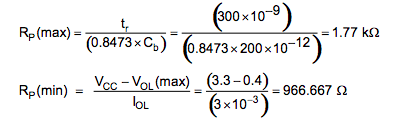
Therefore, we can select any available resistor value between 966.667 Ω and 1.77 kΩ. The value of the pullup resistor can be selected based on the trade-off for the power consumption and speed.
Speed Versus Power Trade-off
Once the minimum and maximum value of the pullup resistor has been selected, the decision for the value of resistor can be made based on trade-off between the speed and power budget. A smaller resistor will give a higher speed because of smaller RC delay, and a larger resistor will give lower power consumption.