| Assignment | Used software | Files/Downloads/links |
|---|---|---|
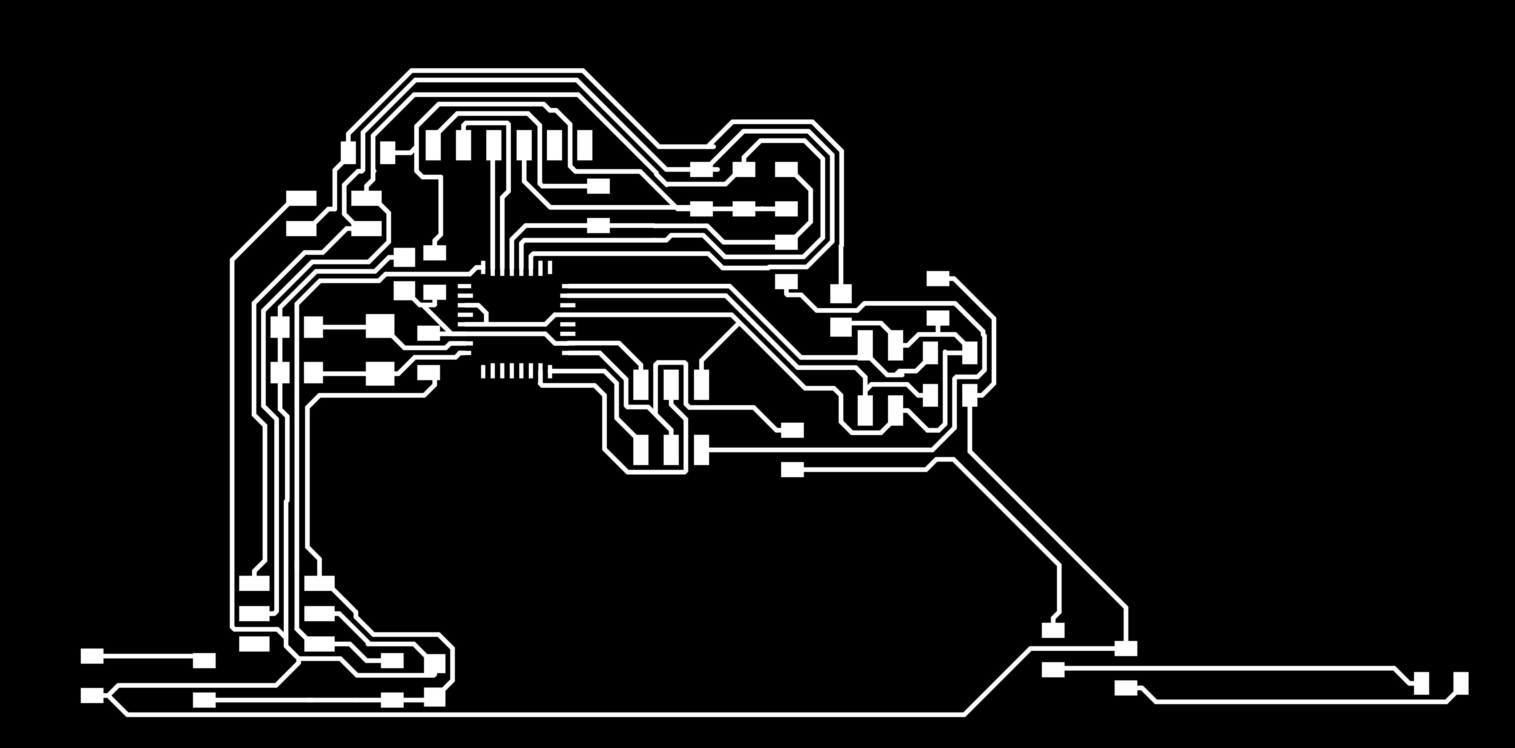
| mil traces | Kicad | skate-F.Cu.png |
| mil outline | Kicad | skate-Margin.png |
| schematic Layout | Kicad | skate.sch |
| PCB Layout | Kicad | skate.kicad_pcb |
Boards for the final project
Connections i need on my final board:
- piezo :
- A0
- A1

- Piezos are polarized, meaning that voltage passes through them (or out of them) in a specific direction. Connect the black wire (the lower voltage) to ground and the red wire (the higher voltage) to analog pin 0. Additionally, connect a 1-megohm resistor in parallel to the Piezo element to limit the voltage and current produced by the piezo and to protect the analog input.

- The sketch reads the piezo output using the analogRead() command, encoding the voltage range from 0 to 5 volts to a numerical range from 0 to 1023 in a process referred to as analog-to-digital conversion, or ADC.
- oled :
- GND goes to ground
- Vin goes to vcc
- SDA to I2C Data (this is A4 on the atmega
- SCL  to I2C Clock(this is A5 on the atmega

- The OLED itself require a 3.3V power supply and 3.3V logic levels for communication.
- The power requirements depend a little on how much of the display is lit but on average the display uses about 40mA from the 3.3V supply.
- battery:
- Lithium Ion Polymer Battery
- 3.7v 500mAh (look if i need a bigger one)
    - Mini usb input Lipo Battery Charging Board
    - Max17043: LipoFuel Gauges
- ftdi:
	- connect at least 3 wires:

- TX
- RX
- RST
Networking I2C
Connected to my board will be 2 shields, that are both connected through I2C: Oled Display and LiPoFuelGauge.
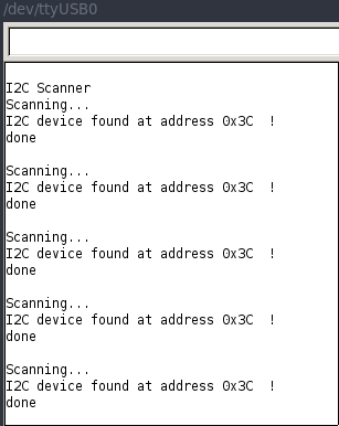
So we need to find the i2c address of the display. To get this, I use a quick i2c scanner uploaded to the arduino. The scanner code can be found on http://playground.arduino.cc/Main/I2cScanner. Copy and paste the code into your arduino IDE, build and upload, and fire up your serial monitor.
The image below shows the I2C address of the oled display. Later on i used the same code to check the address of the LiPoFuelGauge (0x36).
As you can see in the final code i use the wire library to connect to the LiPoFuelGauge shield.
The U8glib library uses its own for communicating with the display through I2C. For the display to work with I2C i had to define the display in my code. For my board this is:
U8GLIB_SSD1306_128X64 u8g(U8G_I2C_OPT_NONE|U8G_I2C_OPT_DEV_0);
It uses the u8g_com_i2c.c library for settings of I2C for the specified board.
Designing the electronics scheme

I first started to design the necessary stuff for running this atmega ic. I already knew a lot because it looks like a standard arduino uno, or more precieze, a fabschoolino, that is used to learn kids soldering.
So first i did VCC and GND, broke out RST with a 10K connected, and the crystal with the belonging cabs (18pf for this crystal). Later on followed by FTDI connector pins and AVRISP headers.
I then bundled the connections:
- one sixheader to the power unit (LiPo fuelgauge board + Solar LiPoly Charger)
- one 4 header for the 2 piezo’s
- one 4 header for the oled
| Gates used at the atmega328 | |
|---|---|
| A0 | piezo 1 |
| A1 | piezo 2 |
| PD2 | charge pin/led connection of the Solar LiPoly Charger |
| SDA + SCL for I2C | to both oled and LiPoFuelGauge |
| RX/TX/RST | for the FTDI |
| SCK/MISO/MOSI | for ISP headers |
| XTAL1/XTAL2 | for the crystal |
Designing the PCB
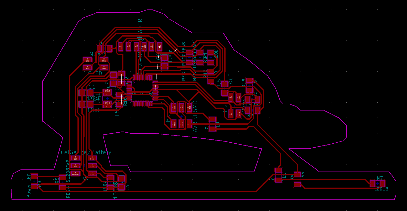
I wanted to make a nice looking board so made it in the shape of an skate :)
Placing and routing went pretty well. At the end i had to use some 0ohm resistors to make all leads. One lead (GND) i finally connected with a wire to cross a bunch of lines.
I did a final check of the schematics and the PCB with zaerc and he suggested to put some resistors between the sda/scl and the atmega, accoring to the I2C specs. But those resistors already appear on both I2C boards so after removing them the boards started working.
Another design mistake was that i forgot to place a 100nF CAP between the RST gate and the FTDI header. Luckily i placed a 0ohm (former labeled as R9) on that lead, so after replacing the 0ohm with the CAP that also started working.
And i wired the TX and RX wrong, but that is not a problem because i use a cheap chinese ftdi with jumper cables, so after changing the wires for TX and RX i could program the board.
| So a summary of the mistakes and solution: | |
|---|---|
| resistors between sda/scl and vcc | Were on the i2c boards, so removing solved the issue |
| 100nF capacitor between FTDI and RST gate | design contained a 0ohm (R9) which was replaced by 100nF acapacitor |
| did not switch TX/RX between atmega and ftdi headers | ftdi with jumperwires to connect right TX/RX |
Milling the board
I had some problems milling the board because after the traces were done, the X-axis of the machine went out of focus and that resulted in a nice cutout trace straight trough a bunch of traces :(
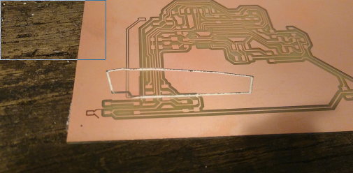
If you look at the picture in the next chapter, you see some strange trace on the right side of the board. At that place the milling only removed the top layer of the copper and didn’t went through the whole copper layer. I was able to cut through the copper and isolate the traces, with a Stanley Retractable Utility Knife. I measured with a multimeter for shorts, specially in that corner, but the cuts did the trick. The mill probably didn’t went completely through the copper on the right side of the plate because the sacrificial layer is a bit slanting. The length of the board is probably also a reason why we didn’t notice it before.
Soldering the board
After the milling was done soldering was on. I started by first soldering all the components that are needed to brun the bootloader and to program. I used PTH crystal and caps because the footprint for the crystal looked wrong.
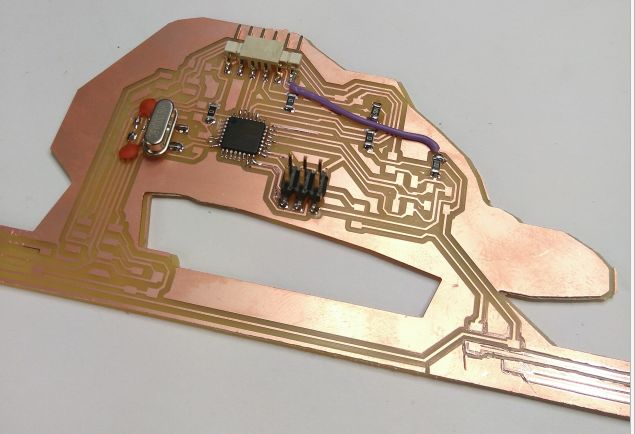
A few hours later Zaerc showed me that the foodprint for the crystal was the right one, and we had that crystal in stock. Both Emma and me didn’t know, so i replaced them, as well of the caps for the crystal (18pF).
I was now able to burn the bootloader but couldn’t program because of the missing 100nF CAP as descibed above in section where i explained the failures i made in the design. So i also soldered the rest and could start debugging.
After making the fixes described above, everything worked :)
I really like this board and the shape. Also the desision to use flatcables was the right one. For the first time, my work is not a cable spagetti :)
BOM
| Material that was available at Fablab Amsterdam / Waag | Estimation of the cost €15,00 | Fab Lab Inventory | ||||
|---|---|---|---|---|---|---|
| Ref | Qty | Value | Footprint | |||
| C1 C2 | 2 | 18pF | fab:fab-C1206 | |||
| C3 C6 | 2 | 100nF | fab:fab-C1206 | |||
| C4 | 1 | 1uF | fab:fab-C1206 | |||
| C5 | 1 | 10uF | fab:fab-C1206 | |||
| IC1 | 1 | ATMEGA328P-AU | fab:fab-TQFP32-08THIN | |||
| M1 | 1 | 16Mhz CRYSTAL | fab:fab-2-SMD-5X3MM | |||
| M2 | 1 | Piezo | fab:fab-2X02SMD | |||
| M3 | 1 | OLED | fab:fab-2X02SMD | |||
| M4 | 1 | FuelGauge/Battery | fab:fab-2X03SMD | |||
| M5 | 1 | AVRISPSMD | fab:fab-2X03SMD | |||
| M6 | 1 | FTDI-SMD-HEADER | fab:fab-1X06SMD | |||
| M7 | 1 | LED13 | fab:fab-LED1206FAB | |||
| M8 | 1 | Power LED | fab:fab-LED1206FAB | |||
| R1 | 1 | 10k | fab:fab-R1206FAB | |||
| R2 R3 | 2 | 1M | fab:fab-R1206FAB | |||
| R4 R5 | 2 | 499 | fab:fab-R1206FAB | |||
| R8 | 1 | 100k | fab:fab-R1206FAB | |||
| R10 R11 R12 R13 R14 R15 R16 | 7 | 0 | fab:fab-C1206FAB | |||
| copper plate | 1 | |||||
| Smooth-on PMC 121/30 | 135 gr. |
| I had all these parts from past projects | Prizes are estimate what they will cost from several vendors | ||
|---|---|---|---|
| Ref | Qty | Datasheet | Prize |
| FuelGauge/max17043 | 1 | MAX17043-MAX17044.pdf | $3.07 |
| Battery | 1 | Li-Polymer 500mAh | $7.95 |
| USB / DC / Solar Lithium Ion/Polymer charger - v2 | 1 | MCP73871 datasheet | $17.50 |
| Display OLED 128x64 | 1 | ssd1306 128x64 | €10.31 |
Improvements for the next version of the board:
-
I noticed i made a mistake somewhere in the whole proces. When you look at the powermanagment page at the wiring of the boards, you see that in the initial plan i wanted to connect PD2 on my board for giving alert to my board when the battery’s SoC goes below a threshold value. What i did at the end was connecting the charging led of the solar LiPo charger board, which has connectors for using an external led, i wanted to connect to my PCB. So somewhere in the proces, probably due to the stress to get things done for the presentation, i mixed up the two. In the next version of the board i will connect the alert pin of the LiPoFuelGauge to PD2 to put the atmega in sleepmode when battery goes below a specifeid value. The charge indicator from the solar LiPo charger board i will then connect to PD3, one of the gates of the atmega that is not used at the moment.
-
another thing that i want to add for the next version of the board is bluetooth connected. It is rather easy to implement because there is enough room in the casing. And the needed connection pins are already there. I need VCC, GND, RX and TX for that, and those pins correspond with the ftdi header pins, that are not needed while operating the device. Hardest thing for me would be to programm software on android to get a kind of program, that listens to the measurements given through bluetooth, and saving that data, combined with time and location.
-
I really would like to get rid of the bypass wire that connects GND of the FTDI to the other GND traces.
-
Replace the sacrificial layer to a complete leveled one so the milling bit goes through the complete copper layer.