Electronics Production
Task:
- Characterize the specifications of your PCB production process
Daniels and Christophs Part:
Getting the specifications of our mill a.k.a. theoretical limits
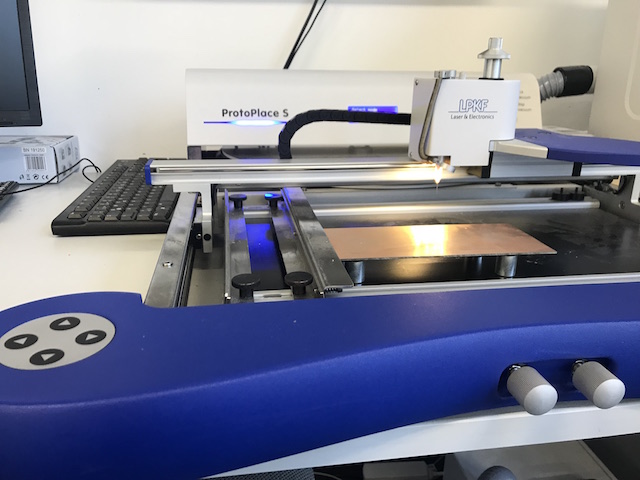
At the HRW FabLab we're using a LPKF S63 for in-house prototyping. This machine is very accurate, fast and realiable.
To characterize the given specifications which the machine offers, the best way is to check the datasheet, the manufacturer supplies.
Let's have a look at the specs:
Max. material size:
This specifies the maximum size of the material, which can be used in this machine.
Resolution:
The resolution is given in X and Y only, because the z axis is free. The Z axis has a fixed depth controller with PTFE surface, which is sliding over the PCB while milling.
To control the depth of cutting, the clamping length of the mill in the collet chuck will be changed automatically, while using a integrated camera to check the cutting width.
Repeatability:
The Repeatability of our machine is good enough to mill PCBs even for small packages like TSSOP, TQFP or other fancy stuff like Nexperia PMZB200UNE MOSFETs, which are 1.05x0.65mm small.
This is a huge advantage as the most new fancy ICs are built into really small packages and can be used without any bulky breakout board or wiring.
Precision of front-to-back alignment:
This value describes the precision from the top to the bottom layer, when milling a double sided PCB. Through the fact that the most through-hole mounted parts have much larger manufacturing tolerances, there is no limitation for using these parts or connect traces on both sides with rivets.
Milling spindle:
A spindle fast like this one, is needed to mill with the small 0.1mm mills with low force. This helps to extend the tool life.
Tool change:
The automatic tool changer saves a lot of time, as you don't have to change all your tools by hand and measure the clamping length after every tool change.
Milling width adjustment:
As I mentioned above in the "resolution" section, the milling width is controlled via camera automatically. This feature prevents a lot of milling fails, as you have to measure the clamping length very accurate.
Tool holder:
Just a standard 3.175mm tool holder system with automatic clamping chuck.
Drilling speed:
The mill is able to drill 120 holes per minute, theoretically.
Travel speed (X/Y):
The rapid movement speed. Not that fast, but far enough for this small material area (2 seconds for the longest one-axis travel).
Practical limits
Official specifications are a good start to get a grasp on the capabilities of a fabrication process. Sadly, they are not always the full truth. While working with our mill, we stumbled upon some very real, practical limitations that can make life hard, and suggest using different process parameters when possible:
First, while the machine can reproduce a set milling width of either 0.2 or 0.1mm and will do so, the CAM software will sometimes straight out ignore separation channels of exactly the set minimum width - Probably due to cumulated errors from unit conversions or some problem like that. We have learned, from that, to just set the minimum separation to at least 0.21mm (we're not using the really expensive 0.1mm mills at the moment), or 0.25mm whenever there is more space, just to be safe.
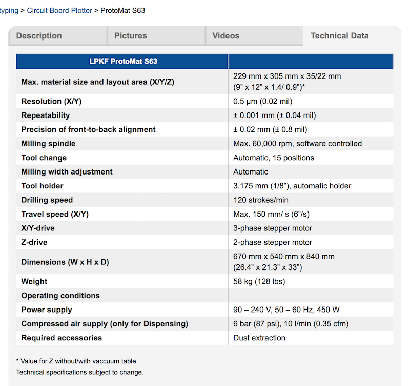
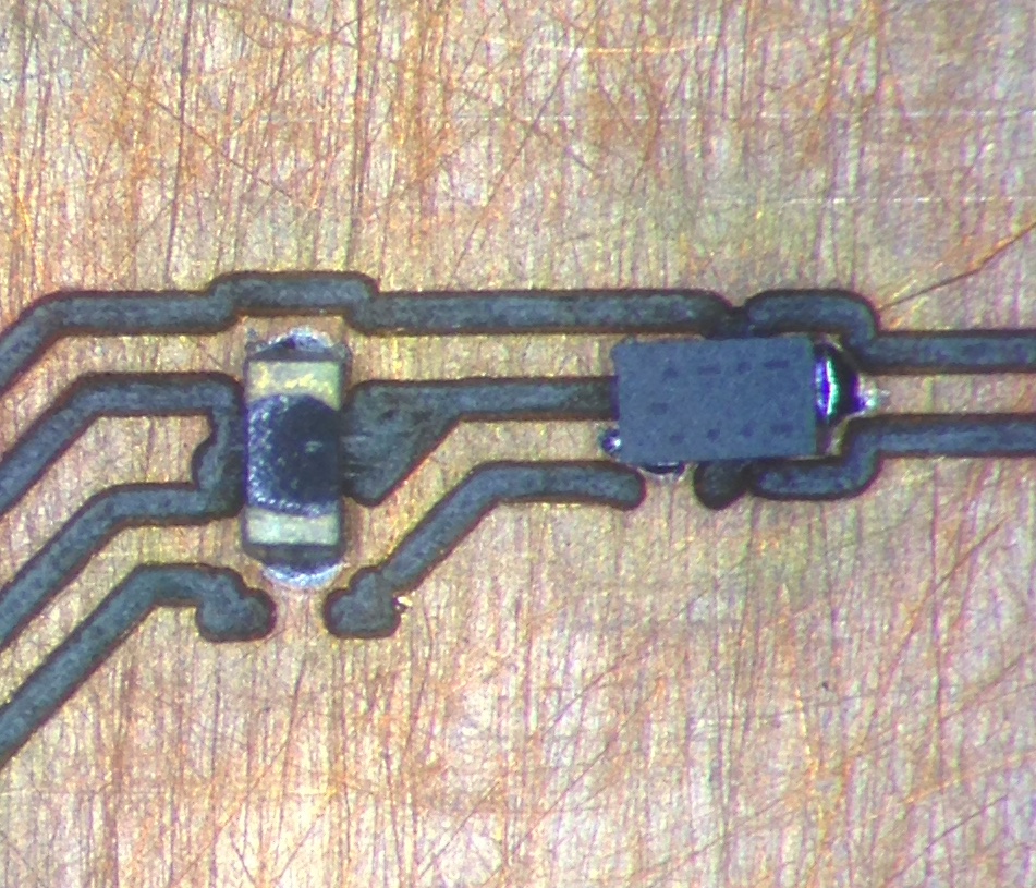
Second, while the machine will set the milling depth correctly and with good repeatability, the resulting milling width of the conical mills changes over time. A look at a worn down mill under the microscope revealed that most of the wear seems to occur in the area that cuts through the copper plating, destroying the conical shape and resulting in more and more unstable milling width settings.
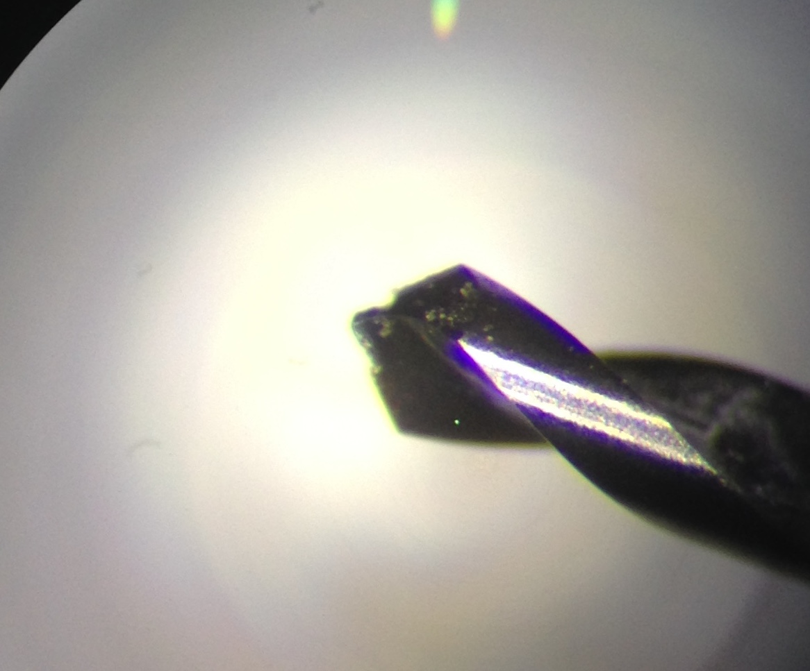
Also, at some point the tip will degrade so much that it doesn't really cut any more, resulting in milling channels with bashed-in, but not separated copper. In the image, the clean cut parts were done with a new 0.2mm mill, while the failed parts were attempted with a worn 0.1mm mill.
To make matters worse, while the machine software will warn you when it thinks a mill is worn, that rating is purely based on usage, and can be way off. The machine has no way to really check a tool's state, so it's a good thing to be wary and have a look with the microscope.
Third, the conical mills will also result in angled walls of the milled channel. The milling width setting of the machine software tries to somewhat hit the middle between the top and bottom milling width, so neither will the milled channel be as wide as specified, nor will a track be as wide (on top) as specified. When going to the limits of small, tightly packed pads, the results can get increasingly hard to actually solder parts onto.
Fourth, while the camera system is nice and quite precise, it can latch on to the wrong hole, so having holes near the fiducials is not a good idea. Planning is everything...
Fifth, dirt is your enemy. Get rid of it. Get it out of the machine, in any way possible. When you set up everything, calibrated everything, put in a new mill, checked the files... dirt will get stuck under the depth controller and ruin everything. Call in an exorcist if you need one.
What we can do
Even with the limitations we found, we managed to get some nice stuff to work. One example is a nice and small MOSFET in a case the size of a 0402 resistor:
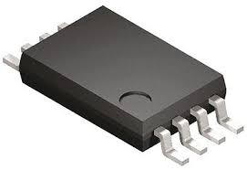
There are, of course, three pads under that 1x0.6mm package. We used something like 15 of them as of now, all of them with manually applied solder paste, and had no shorts. It's quite a lot of work to get that small amount of solder paste applied (with the tip of a scalpel), but it works.
Another example is a 0201 capacitor we used - Mostly to see if it can be done, and, of course, for shits and giggles. That larger resistor is a 0402... And an edge of a QFN case next to it.
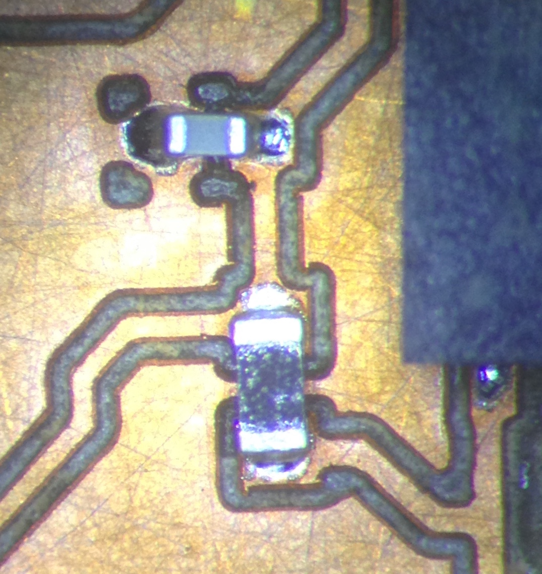
We also tried hand soldering a 0201 to see if it works. It... kind of works. Under the microscope, on a good day. It's no fun, though.
Downloads
| No Downloads here |
Lukas's Part
Eagle Process
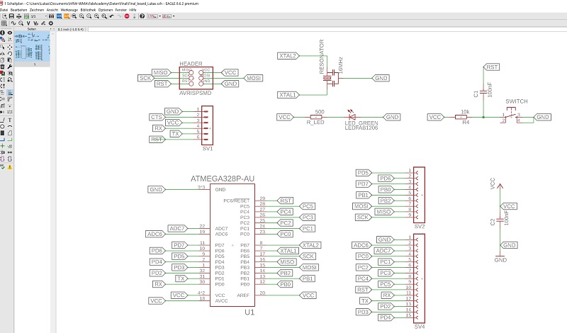
I used Eagle 8.6.2 for my board development. For students and scientific research assistants is this software for free. It uses the same login dates like Fusion 360, cause it is also a Autodesk tool. I´ve never worked with eagle before so I had to install it first. The installation is quite simple, and there is no additional explanation necessary.In Eagle the first step is always to develop a scheme of your platine. Here it depends on what you would like to make your board do. You need a lot of electrotechnical knowledge to generate a working scheme. There are a lot of standard components in the library you can simply add in your scheme and wire it.
At the end you are able to do a logical check if there are any problems in your scheme. See here a typical scheme of a Arduino-rebuild in Eagle :
Now you can develop your board layout. Therefor you change to the Eagle board design function. Eagle generates the single footprints out of your chosen components and connect the different pads like the scheme. The first quite useful step is to make the complete board GND (ground). Now a lot of connections between components disappeared. The next step is like a puzzle and you need a little bit of experience to generate a functional layout. Here it is smart to start with one component with a lot of connections and place the rest of the components around it und rotate and move them until the lines didn´t cross anymore. Often you won´t find a solution without crossing connections. Now you have to start wiring the single connections. See here the finished board-layout of the Arduino-rebuild of the scheme above:
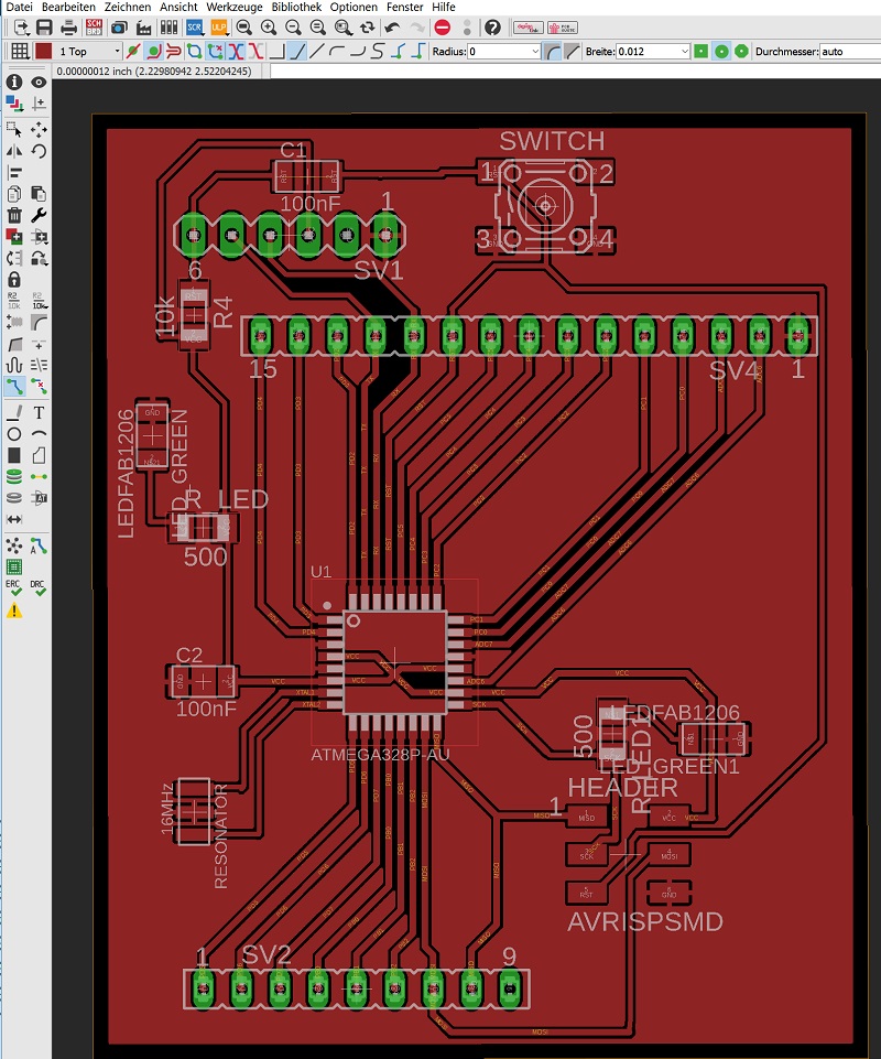
With this design you ca go on with the CAM prozess. See this step below.
Tanja's, Part:
Picking and placing the components
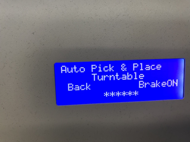
Protoplace is a semi automatic pick and place turning table. You can despence the soldering paste semi automatic. For this we use the function "Auto Pick and Place" and "Brake On" for precise positioning of the despenser.
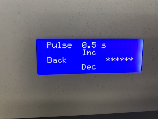
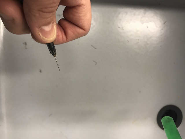
For the right amount of the soldering paste it is possible to set the dispensing time. E.g. "0.5 s" is good for bigger traces like footprints for header. For the chip footprint it is better to set the despenser to 0.3 s. You also have to take care about the size of the needle.
Dispenser above the plane board.
Now it is time to place the components. We should notice the right orientation of the MCU and the LED. MCU has an circle sign on the top. We should compare it with the pinout of the MCU to position it right. LED has a greeen point which should be oriented to the GND. Z-Diode has a mark which should be oriented to the signal trace. Resistors and capacitors have no certain orientation.
AtTiny45 Pinout, but notice that the real MCU has the sign on the corner.
After finishing the picking and placing one schould allways clean the despenser needles using compressed air until the air is going through.
Peter's Part
Isolation milling
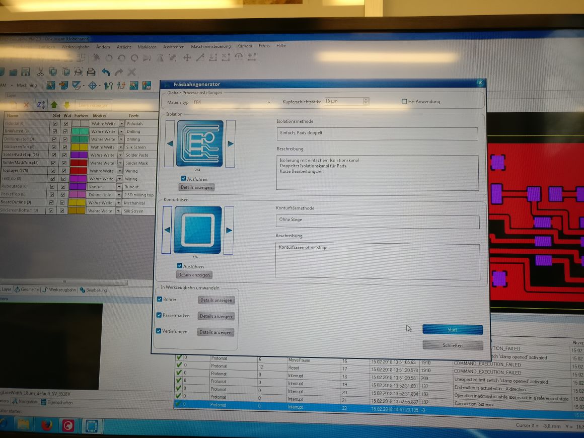
After I created and exported the Eagle files.
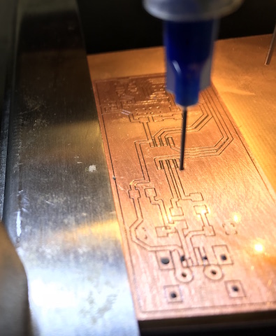
I start milling.
In our lab we use an LPKF isolation cutter.
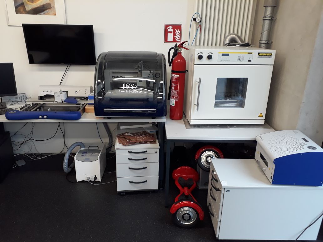
our electronics corner with the LPKF...
Basic setting of the PCB material in the LPKF.
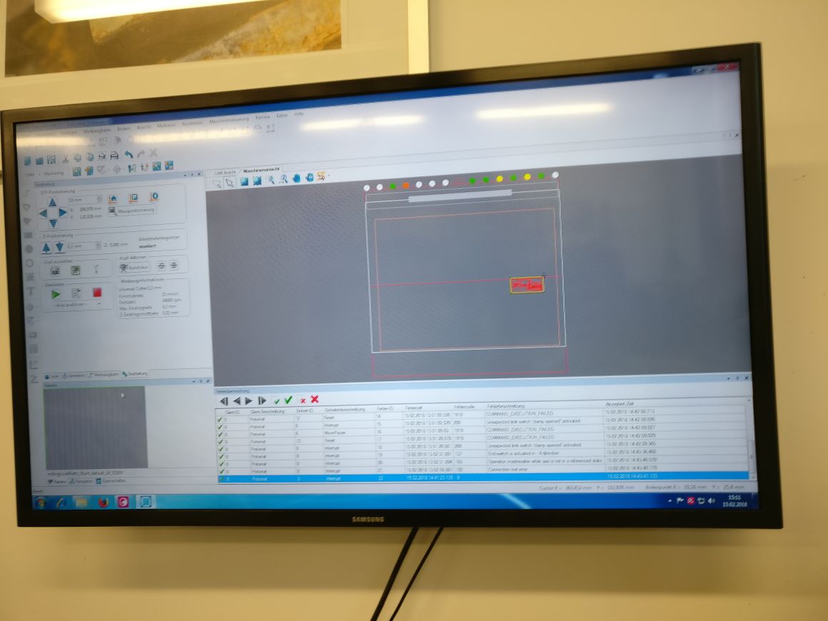
Positioning device on the board.
Then I milled the board.
I cleaned the finished board and sprayed it with solder varnish.
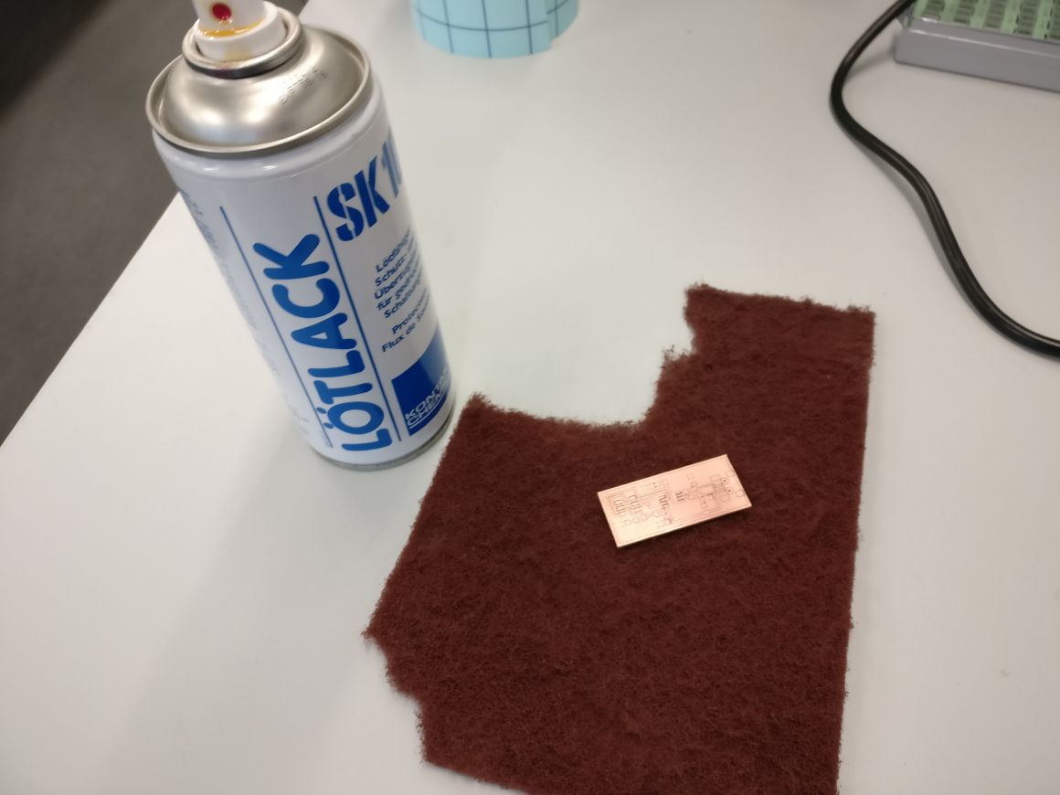
...cleaned and sprayed with solder varnish..
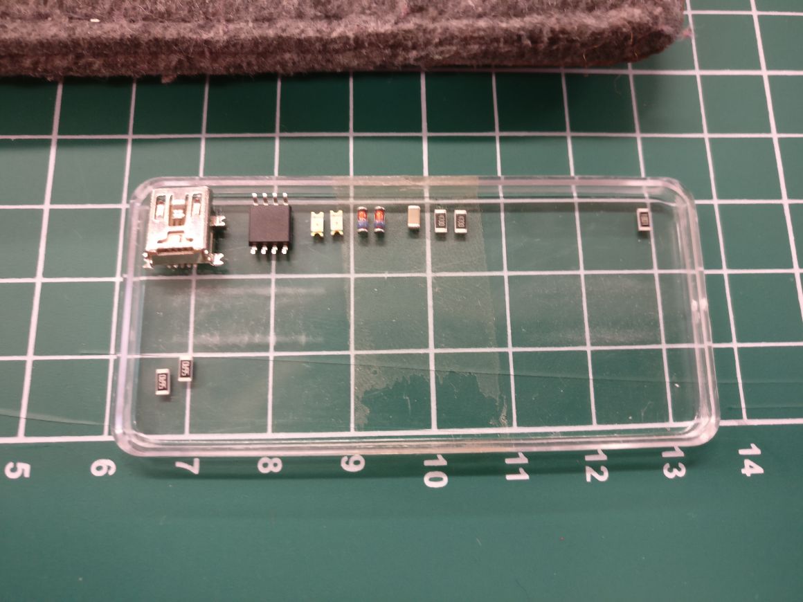
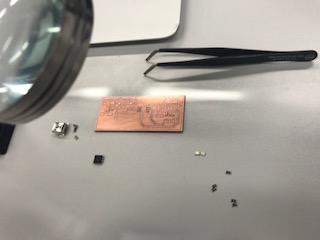
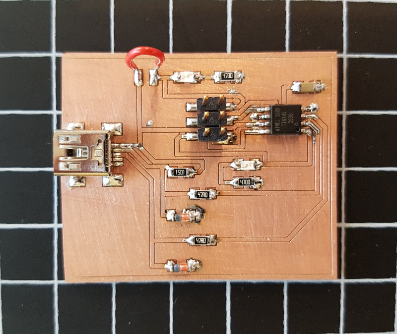
Put out the matching parts.
Equipping and programming
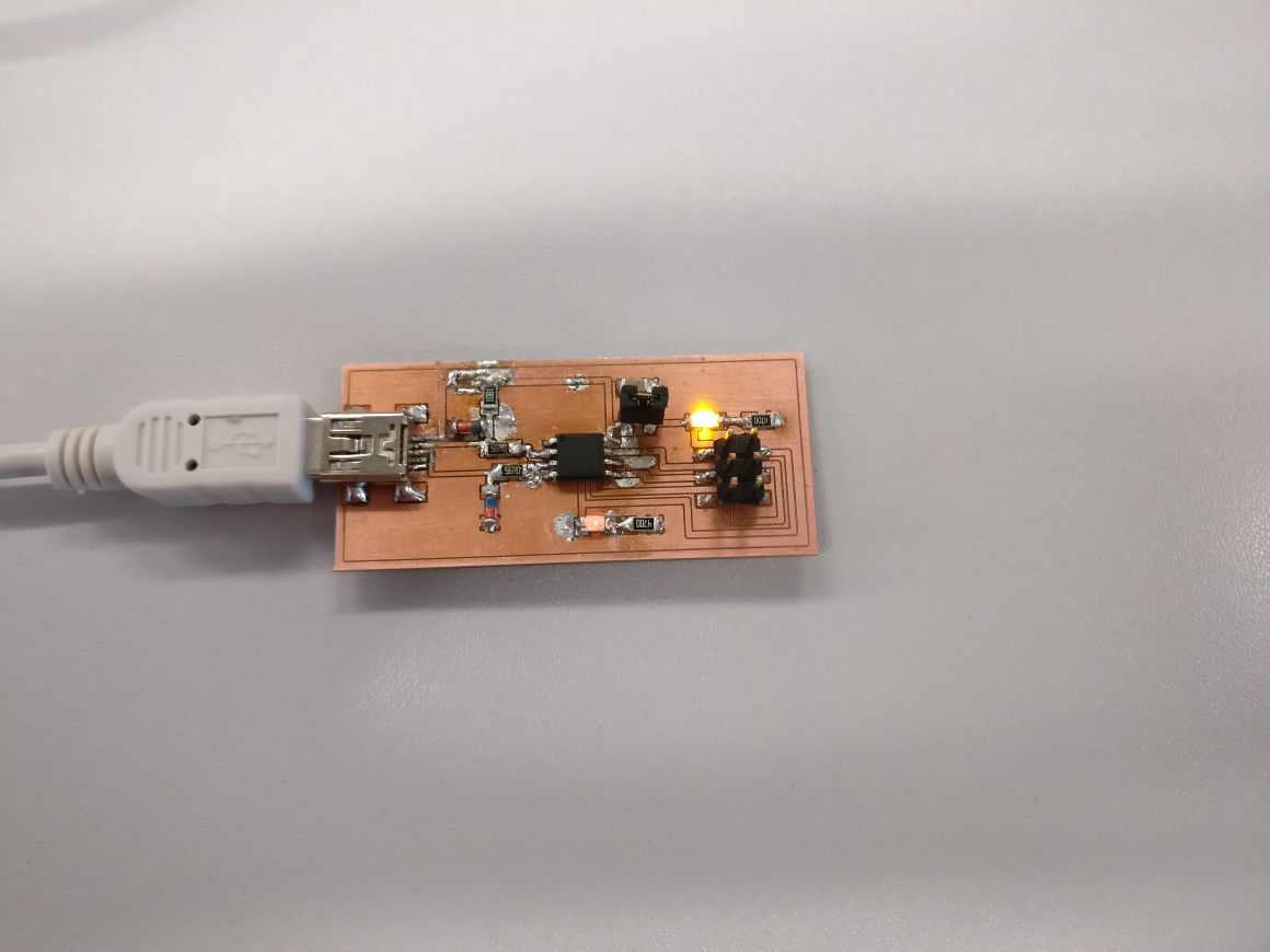
Finished board first test on fused 5V.
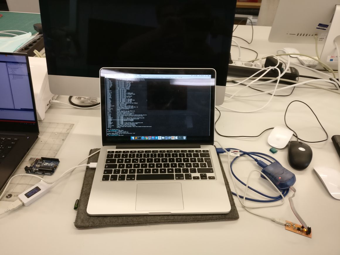
Programming construction.
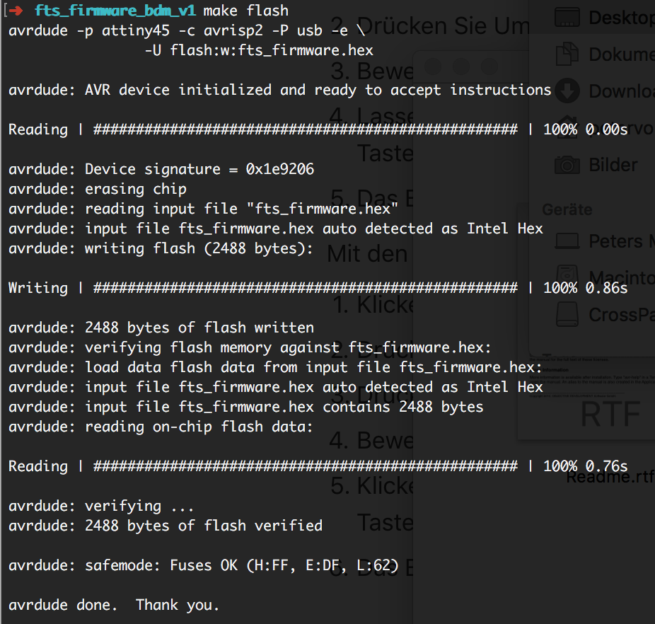
successful flashing...😅
I could also successfully set the fuses.
So far everything worked out but from now on the problems came.
He was not recognized by my Mac on a Win PC he was recognized but I was not able to address him.
Unfortunately, I can not continue at this point.😢
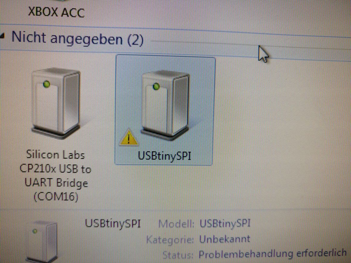
The recognized FabTinyISP whose drivers can not be loaded😢
Jimena's Part
Soldering
Soldering is the process of using a filler metal (solder) to joint at least two metal parts/components together. The solder has a low melting point and allows current to flow between the parts.
What do you need?
Before we started soldering the PCB, we checked if we had everything we need:
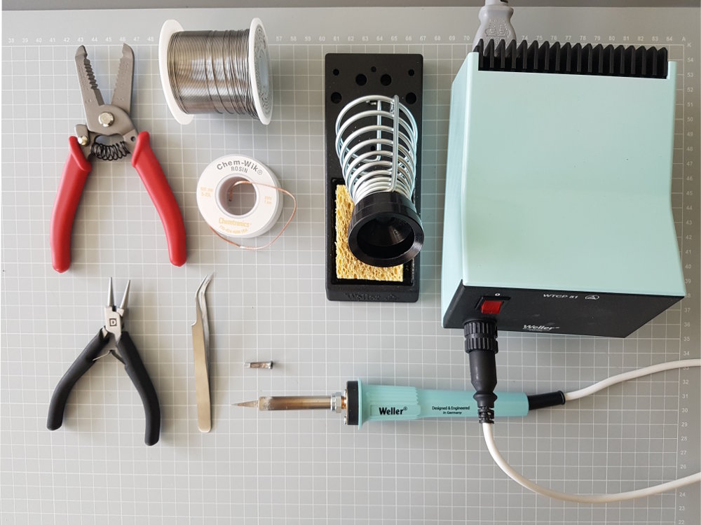
- Third-hand tool or vise: to hold the items you’re soldering.
- Soldering iron station with soldering stand and cleaning sponge:
You use a wet sponge to clean the soldering iron tip. The tip has to bee always shiny. Conical pointed tips are better for detail work.
We recommend a soldering iron with a variable temperature control. You can damage your components on your PCB while soldering, if you use a too powerful soldering iron.
- Lead-free solder: We recommend thin solder for detailed work: 0.5mm (0.020”) to solder SMD components.
- Tools: Wire stripper, wire cutter, needle nose pliers, tweezers
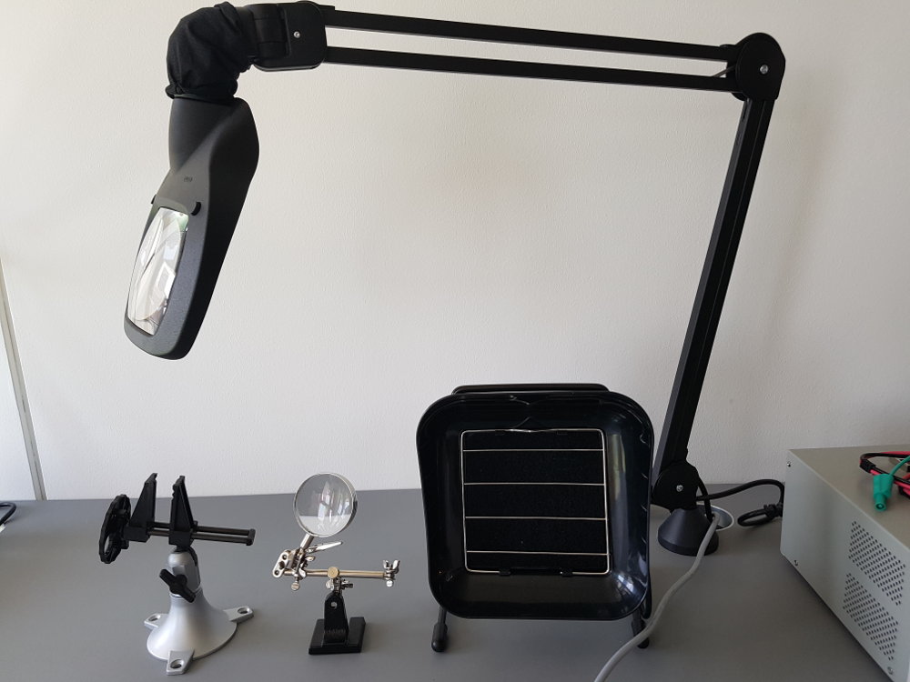
- Magnifying glass: for a better look at your project. We used a top desk magnifying glass with LED light.
- Desoldering braid: Solder can be re-heated, You use desoldering braid to undo soldered joints.
- Exhaust fan/ventilation with filter
- Eye protection: always when soldering!
- Parts you want to solder: before you start soldering make sure you have all the components you need, for example microcontroller, resistors, capacitors, wires, and so on.
Soldering Process | Assembling the PCB
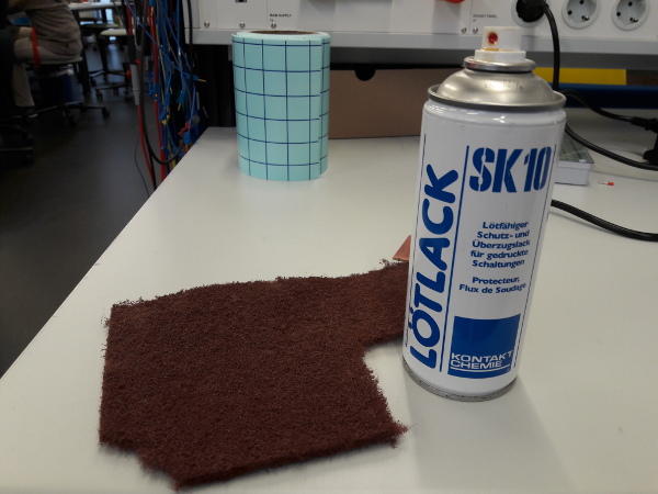
- Before we started soldering the components on the PCB you had to polish the surface with a metal-free, ultrafine board cleaning pads to remove the oxidation
residues from the copper layer on the base material. After that we used a soldering lacquer for the final finish, it has to dry for about 10 minutes.
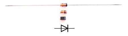
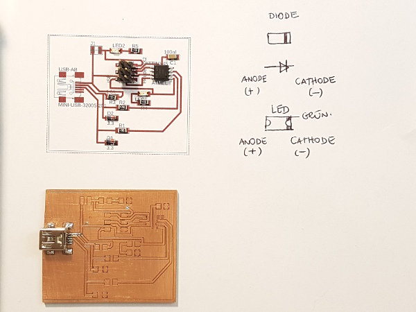
- Next, we recommend printing the layout of the PCB and placed the components in the right place and direction. If you don’t know which is the right direction, check the sketch (photo) about the anode and cathode in the diode and LED.
- Turn on your soldering iron and wait a couple of minutes until it reaches the set temperature. Then clean the tip with the wet sponge.
- At first, we put some solder on the hot tip, then heated the joint with the soldering iron tip.
You have to wait until the joint heats and add slowly solder to the joint. The solder will melt and flow properly to the metal parts.
When you’re finished, the joint should be shiny and smoothly.
- Tests: you can start making some tests with wires or cheap components on a board you don’t need.
- If you are ready and have a soldering station with a variable temperature control, set the temperature for your components: 20 – 30 Watt for PCB or IC, … and start soldering!
- Desoldering a joint: we put some solder on the tip first, so that the heat would spread better on the desoldering braid and the desoldering braid
‘absorbs’ the solder you want to remove easily.
Caution: the desoldering braid gets hot very quickly. We recommend tweezers to hold it on the joint.
- At last, don’t forget to clean up and turn off the soldering iron.