final project -- weekly assignments -- about me -- fab academy
Interlude: Stuffing Boards
Making blank PCBs is just one step for actually making electronics. Getting components soldered onto them is a different beast, and one that can make more than its fair share of problems. During Fabacademy 2016 I had to make new electronics for a robot in one of our labs, so Daniel and I took the opportunity to take a set of photos of the process I use. So, while it is by far not a universal solution for everyone, it does work for us, so it might be interesting for others.
This whole process assumes that you are soldering SMD components, including stuff with pads underneath them (like most QFN packages). Tight BGA packages are a different kind of beast, again, and I don't have the experience with them to give any kind of recommendation about tackling them. The LGA in some of the pictures works fine, but has much larger structures than a BGA.
Stuffing Boards
Solder Paste
Solder paste is a mixture of tin powder and flux, mixed to be a sticky paste that will melt into tin when heated. There are different ways to apply it - Industrially, it is usually printed onto the boards using metal masks called stencils, or printed onto the boards using special inkjet printers. There are also application tools to do it by hand, with varying degrees of automation and precision. In the most simple case, a needle or the tip of a scalpel works fine, too.
For the robot parts, I had the luxury of professionally fabricated boards and stencils, but that doesn't need to be the case at all - It is easily possible to laser cut a stencil from plastic (preferably 0.12mm thick plastic) to use on a milled PCB. I've done that, but not in a nice photo session leading to good pictures... Industrially, stencils are made from stainless steel, which is not that easy to cut, but will last way longer than the usual run of one to ten boards I have:
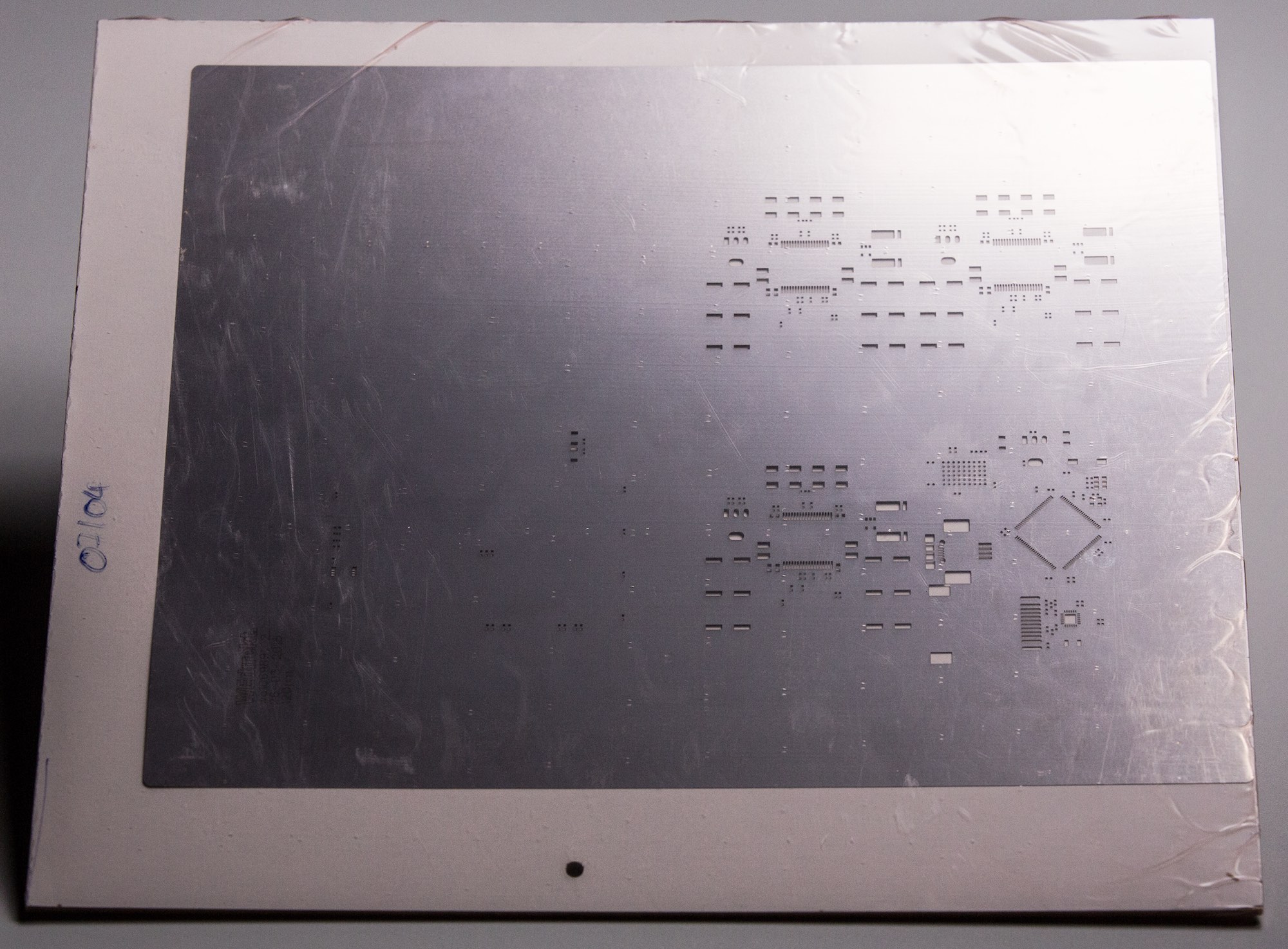
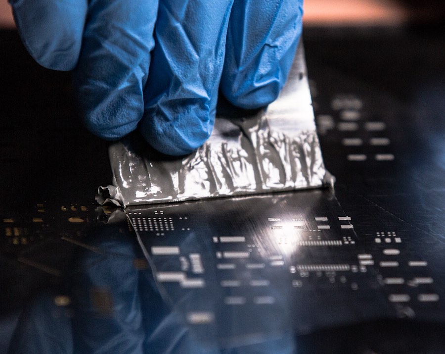
The stencil needs to be fixed in place to the PCB, so solder paste will end up in the right places an not all over the board. Industrially, stencils are usually fixed to a metal frame, slightly stretched so they don't buckle, and then pressed to the PCB using a standardised fixture. I don't have such a fixture, of course, as they are quite expensive, so I buy stencils without frames and fix them in a slightly simpler way. First, I tape some old or otherwise spoiled pieces of PCB material to the table, fixing the PCB in place:
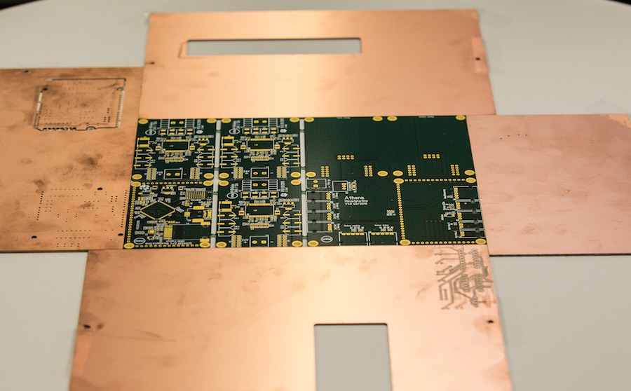
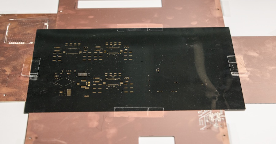
Then, I carefully align the stencil, and tape it to those scrap PCB pieces. It is a good idea to leave a "flap" in one of the tapes so it's easier to tear off, but I usually forget...
Solder paste... I bought solder paste that can be stored at room temperature, is lead free and uses a somewhat less toxic flux. Expensive stuff, but I really, really hate playing with my health. Any kind of solder paste you use should be stirred before use, as they tend to settle and unmix.
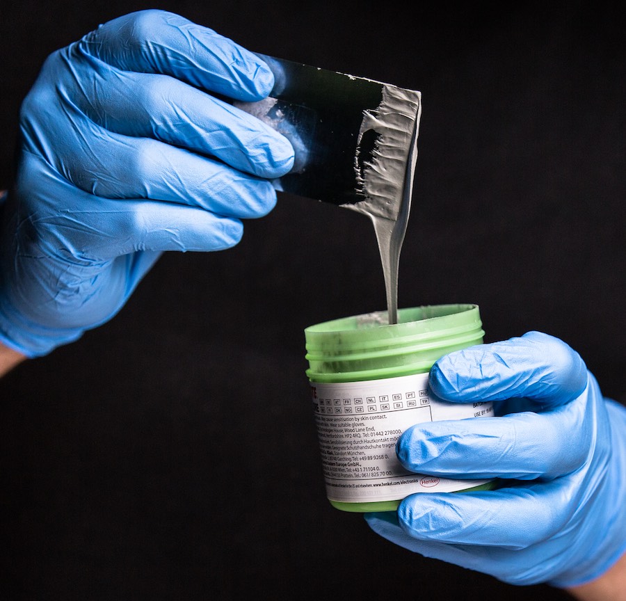
I usually use a simple, cheap scraper to apply the paste. An old credit card or one of the many other plastic cards will work fine, either. I take solder paste from the container, put it onto the scraper, then pull that scraper over the stencil, pressing down with a significant amount of force to get the stencil tightly onto the board. Doing too many passes will usually make the stencil move slightly, smudging everything and leading to bad results, so having a larger scraper than I had in those pictures would have been way better. It worked, though.
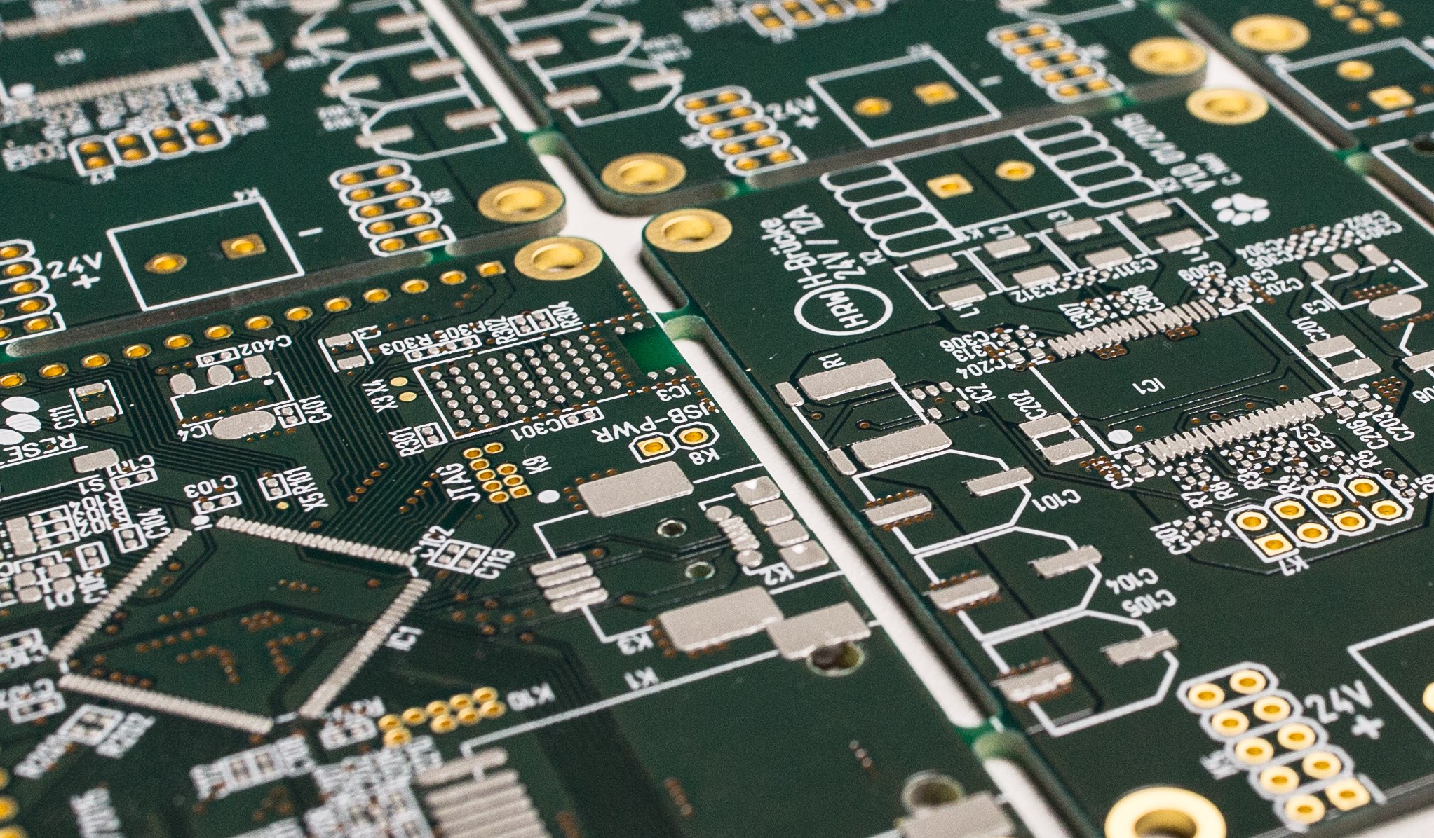
The result should be solder paste exactly on the pads, and no solder paste elsewhere. The result here is not perfect, as there are slight bridges between some of the closer set pads, but it worked out fine. In this case, the soldermask on the PCBs helped, of course - It's not only a coating for the PCB, but also highly repellent to tin. With components that have legs, resulting bridges are relatively easy to correct using solder wick, while on the other hand, QFNs and other legless cases tend to be very forgiving, as the tight space between the plastic of the case and the plastic of the PCB too narrow and the surfaces too repelling for tin to seep into. This part is a little harder with milled PCBs, though.
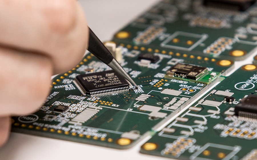
Next, components have to go into their places. Since I haven't found a well-working mechanical placer for my needs, I usually use tweezers of different sizes. Usually, I will place large, "accident prone" components first - Like large ICs of any kind, jacks of any kind, and large or heavy inductors. That leaves room to start over with little loss if anything goes really wrong with those. I sometimes do differ from that routine, though, when I feel like placing something like a USB jack will hamper my ability to reach parts of a PCB, in which case those components will go on last.
It is a valuable help and a lot less hard on your eyes to use a microscope or at least a large magnifying glass for that - For the photos, I did not, but that's to have the space for taking photos.
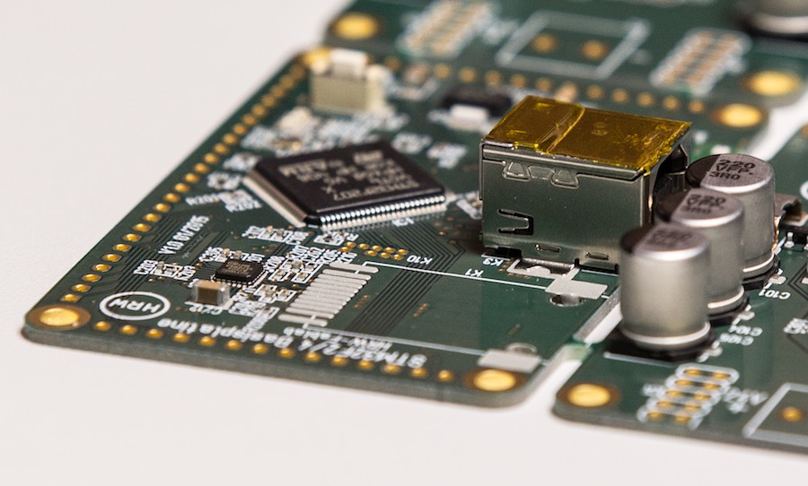
After what feels like an eternity of placing components, everything is on, and the board can go on into the oven.
There are, again, a lot of options here. I did my first boards, some 15 years ago, in a normal household baking oven, heating it up to (very roughly) 275°C and then putting the boards in, watching for when the solder paste melts. That is, of course, a massive health risk you shouldn't take, and very imprecise in temperature control. For now, I use the drying oven at our chemistry lab (set to 265°C, still watching for the solder to melt, with times around 2.5 to 3 minutes). The fablab also has a small reflow oven, which has the massive advantage of automatically going along a predefined temperature profile and sticking to that with good precision and repeatability. It is rather expensive, but something that a fablab doing lots of electronics can invest in good conscience.
What Will Go Wrong
There are, of course, things to go wrong. And they will go wrong, as things always do. One of the most common problems are solder bridges - Tin has an enormous amount of surface tension, so it will creep into any tight area with the right surface, like between the legs of a QFP:
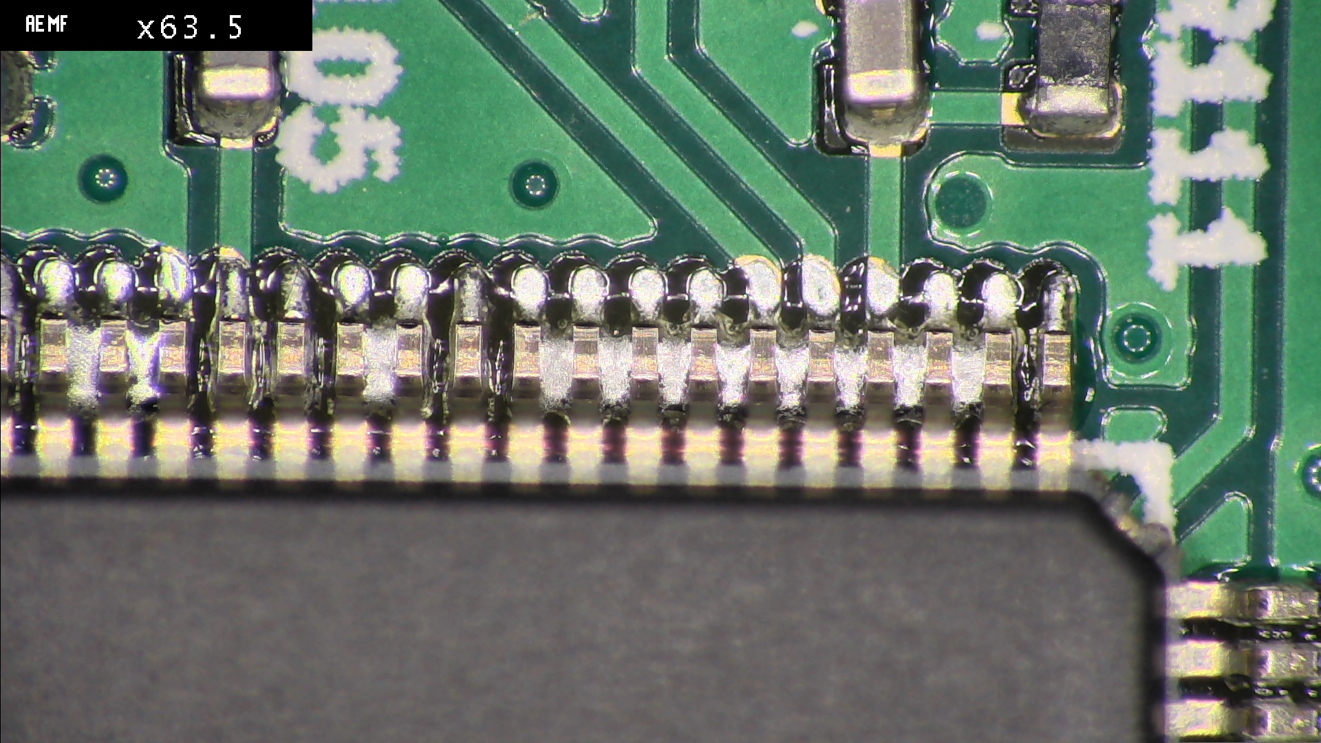
The solution, in those cases, is easy: Put the end of a strand of solder wick onto the pins, and heat through it until the tin melts - You can see that from tin becoming visible in the solder wick, and / or from the matte pins changing to molten tin shine. There is no easy, hard rule, you have to experiment a bit to learn.
A nice effect of this possibility is an easy way to solder some chips without a stencil: Just put a "dam" of solder paste onto the PCB covering all pads along the side of a chip, then suck out excess tin after baking it. That only works with rather robust chips, of course, as it will give them more than a bit of heat.
Another problem not only when using stencils is having way too much solder paste on the board. With most parts like resistors, capacitors and everything "leggy" in general, it won't really matter, apart from more bridging problems. For some parts, though, things can get interesting:
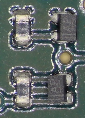
While the area covered by solder paste is usually smaller than the pad, and 0.12mm thick, that small an amount is almost impossible to manually apply, so having way too much paste is a normal thing when applying by hand. In the case above, the openings in the stencil were just twice their intended area (due to wrong design rule settings in Circuit Studio). The resistors, on the left, look rather normal, while the two little diodes on the right (they only have pads in the bottom, with no metal whatsoever at their sides) really don't cope well with it. They swam up (tin has really, really high surface tension, so it wants to ball up... and those diodes really don't pack any relevant weight) and tilted off to the sides. Which is acceptable, in that special case, as they are still connected, but it will degrade mechanical stability. And, of course, it looks bad.
final project -- weekly assignments -- about me -- fab academy
