
Task:
GROUP assignment: characterize the
specifications of your PCB production process
INDIVIDUAL assignment: make an in-circuit programmer by milling the PCB, then optionally trying other processes.
PCB: Printed Circuit Board
Characterize the specifications of your PCB production process
Make AN IN-CIRCUIT PROGRAMMER
EAGLE
EAGLE stands for Easily Applicable Graphical
Layout Editor. EAGLE is a scriptable electronic design automation (EDA) application with schematic capture, printed circuit board (PCB) layout, auto-router and computer-aided manufacturing (CAM) features.
For the layout of the PCB we use EAGLE from Autodesk and install the software in our laptops.
You can follow the instructions from Autodesk to install the software on Linux, Mac or Windows :
After that, you have to create a new project in the Control Panel of EAGLE. If you want to change the directory for the projects you have to go to >Control Panel >Options >Directories.
We became an EAGLE file from our instructor with a template for the layout of the PCB. Each student have to move the components and adapt the template so that there are no shorts. EAGLE shows this kind of errors automatically.
It is also important not to place the components to close as possible. You will need the place for soldering.
I found these tips to design/layout a PCB:
I open the file with EAGLE and switch the interface to
Board to start the layout of the PCB.
- Set the width for the route: 0.024
- Draw a rectangle with the Polygon tool around the components and named it (GND).
- Use the commands 'Route' to link the components or 'Ripup' to undo these.
- Check errors with >Tools >DRC and proof the defaults settings.
- Reduce the area to be cut out with “Move”
- To check the size of the PCB and the place for the components print the layout >Print
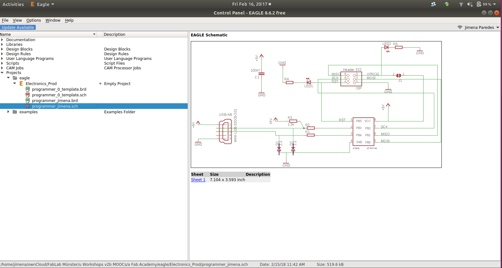 Eagle: Control Panel, new Project
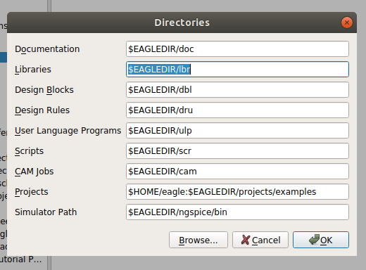 Eagle: Control Panel, Directories
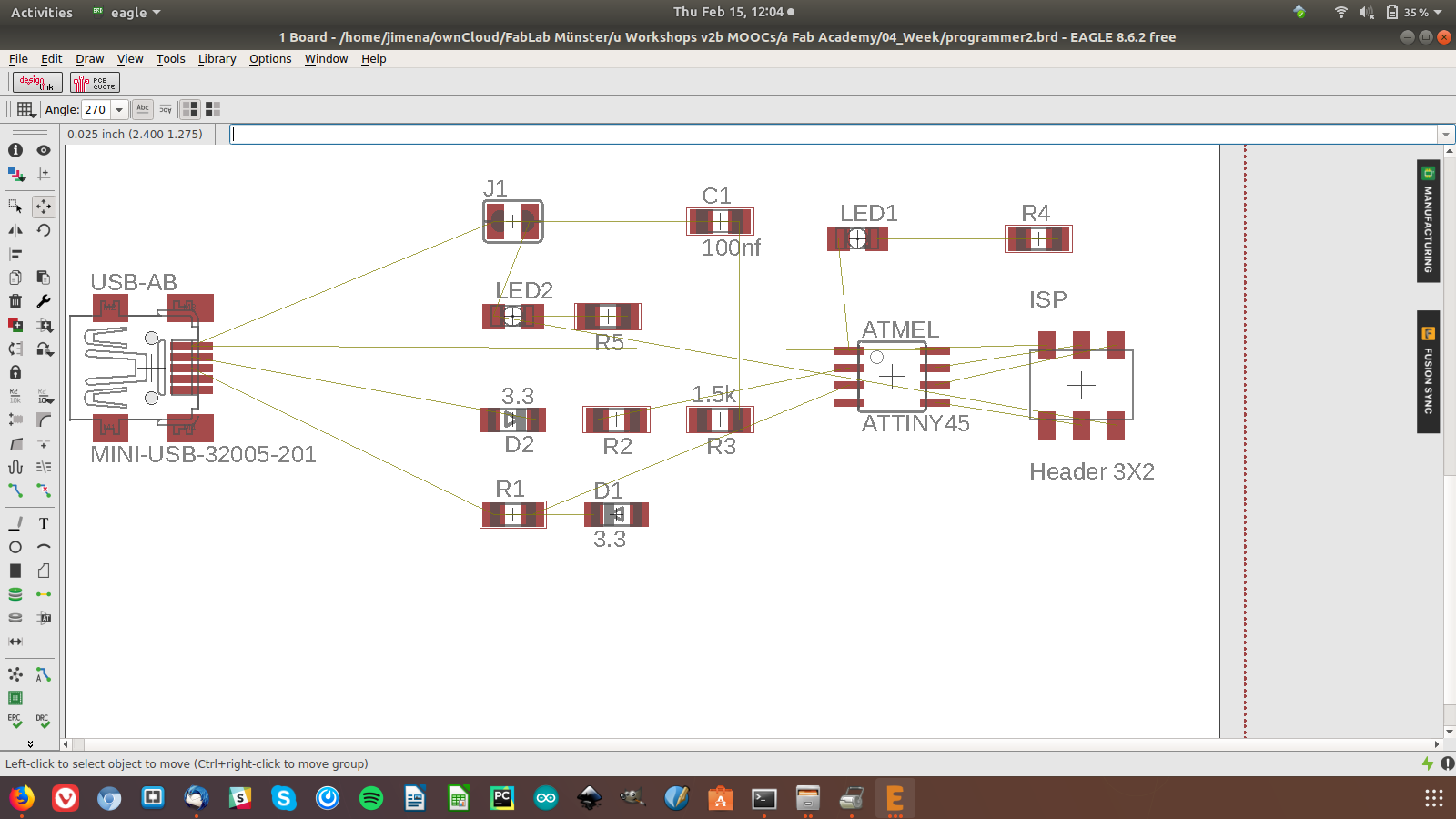 First try
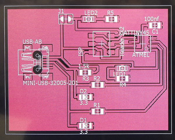
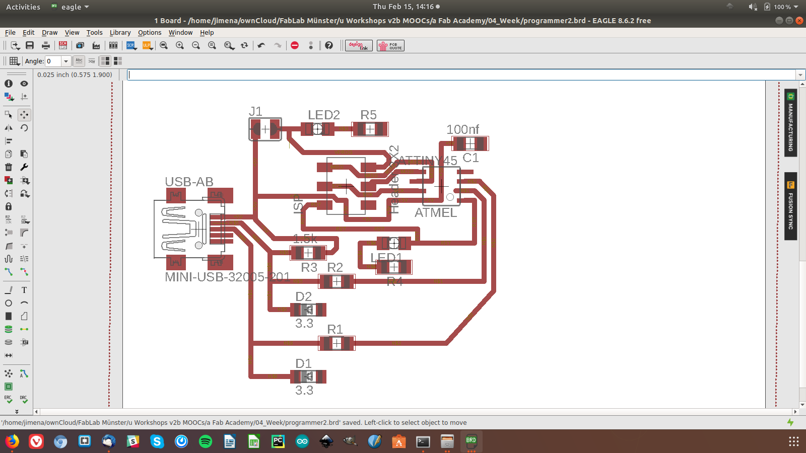 Final version
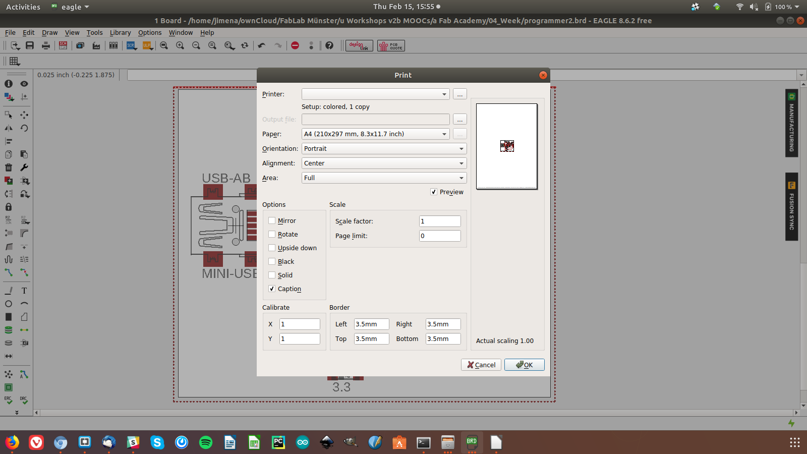 Print the layout
 PRINTING THE PCB
For the milling process I'm using the circuit board plotter
LPKF ProtoMat S63, which is used for any job in in-house prototyping. The ProtoMat S63 masters 2.5-dimensional material machining and features a faster spindle speed of 60.000 rpm. This also makes it suitable for drilling test adapters and housing production.
- Open the EAGLE file with the software of the circuit
board plotter “Circuit Pro” and export a LPKF-file.
- Open the “Cutting Generator” and enter the settings or choose a Template. I entered these settings:
Material: FR4,copper layer: 18 µm, Isolation: Single, double Paths, then press Start.
- Set the origin for the job.
- After the settings you save the file and send the data to the plotter…
- The circuit board plotter use three different end mills: 1x for the mini-USB pins, 1x for the paths, 1x for the PCB borders.
- The circuit board plotter use different end mills and has an automatic tool change bar. Important: you have to check that the open end of the milling tool always stays in the right position (doesn’t rotate).
Material:
Base material is FR4 with a layer of thin copper foil (only one side). Thickness 1.6 mm.
 PCB layout
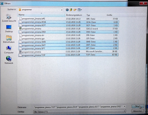 Milling Settings
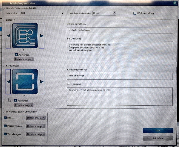 Cutting Generator
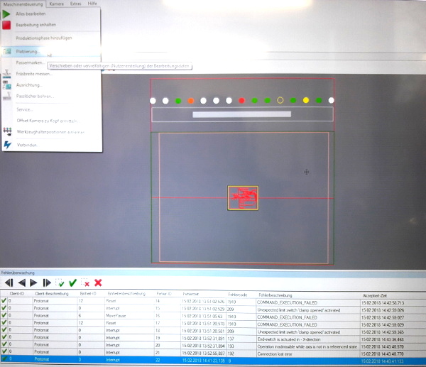 Origin point for the start
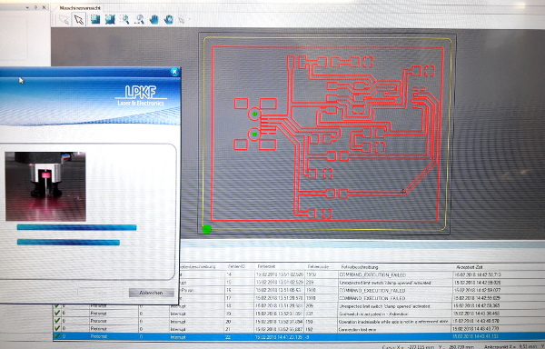 Milling process
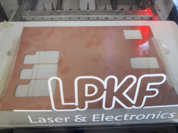 Milling
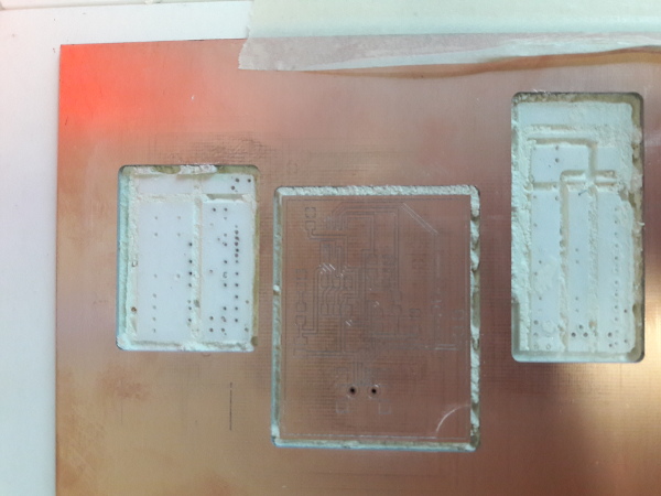 Milling finished
 USING THE MULTIMETER TO CHECK THE PCB
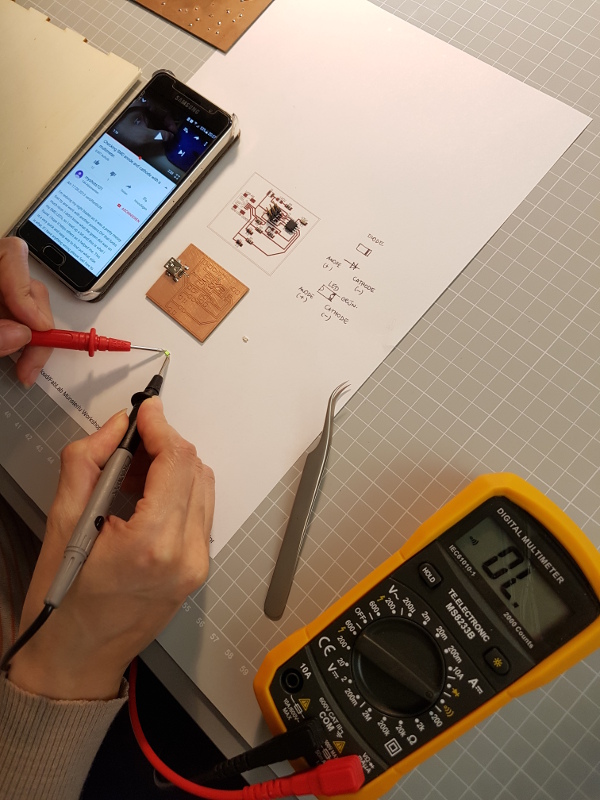
Check the continuity of the electrical pathways with a multimeter. Turn the multimeter to the desired test function and check if it is in working condition by touching
the both probes (test leads) together. Most multimeter will beep or show “0” or a low value on the display. Place the probes on the connection points and should hear a beep. If there is no connection, the display will show OL.
It is also important to check each component, if it’s not damaged.
 Using the multimeter
 COMPONENTS FOR THE PCB
| R1 | resistor 47 Ohm or 50 Ohm |
| R2 | resistor 47 Ohm or 50 Ohm |
| R3 | resistor 1.5 kOhm |
| R4 | resistor 470 Ohm or 500 Ohm |
| R5 | resistor 470 Ohm or 500 Ohm |
| LED1 | LED, orange |
| LED1 | LED, green |
| D1 | Diode 1 |
| D2 | Diode 2 |
| ISP | Pin Heaser 3x2 |
| C1 | Capacitor 100mf |
| J1 | Jumper |
| ATMEL | ATtiny45 |
| USB-AB | Mini USB connector |
 Checking the components
 ASSEMBLING THE PCB | SOLDERING
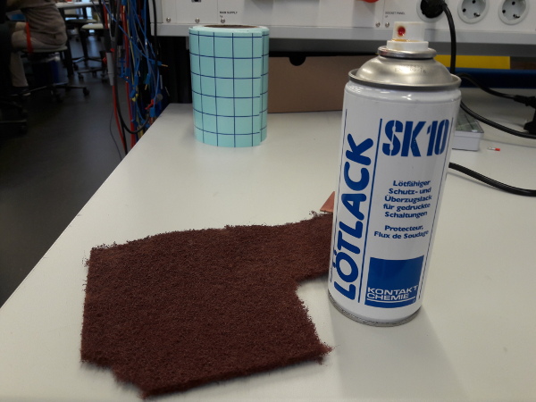
- Before you start soldering the components on the PCB you
have to polish the surface with a metal-free, ultrafine board cleaning pads to remove the oxidation residues from the copper layer on the base material. After that you use a soldering lacquer for the final finish, it has to dry for about 10 minutes.
- Next, I recommend printing the layout of the PCB and place the components in the right place and direction. If you don’t know which is the right direction, check the sketch about the anode and cathode in the diode and LED.
To understand the values on the SMD resistors I found this 4-digit value calculator.
Soldering:
- Turn on your soldering iron and wait a couple of minutes until it reaches the set temperature. Then clean the tip with the wet sponge.
At first, you have to put some solder on the hot tip, then you heat the joint with the soldering iron tip.
You have to wait until the joint heats and add slowly solder to the joint. The solder will melt and flow properly to the metal parts. When you’re finished, the joint should be shiny and smoothly.
- Tests: you can start making some tests with wires or cheap components on a board you don’t need.
- If you are ready and have a soldering station with a variable temperature control, set the temperature for your components: 20 – 30 Watt for PCB, IC, … and start soldering!
- Desoldering a joint: you have to put some solder on the tip first, so that the heat would spread better on the desoldering braid and the desoldering braid ‘absorbs’ the solder you want to remove easily.
Caution: the desoldering braid gets hot very quickly. I recommend to use tweezers to hold it on the joint.
- At last, don’t forget to clean up and turn off the soldering iron.
If you want to know what you need before you start soldering, check our Group Assignment Site:
 Cleaning pad, lacquer
 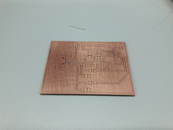 Ready for the soldering
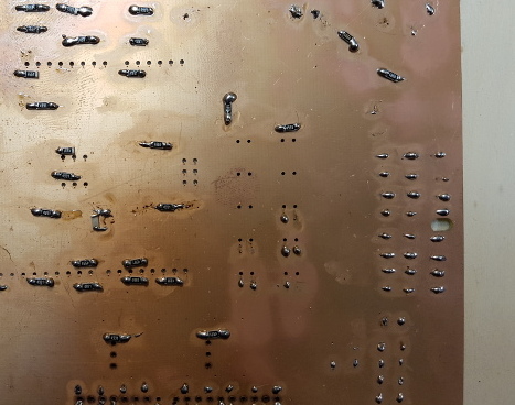 Soldering tests
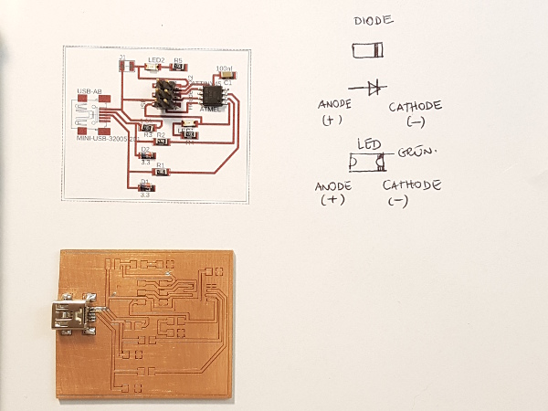 Placing components
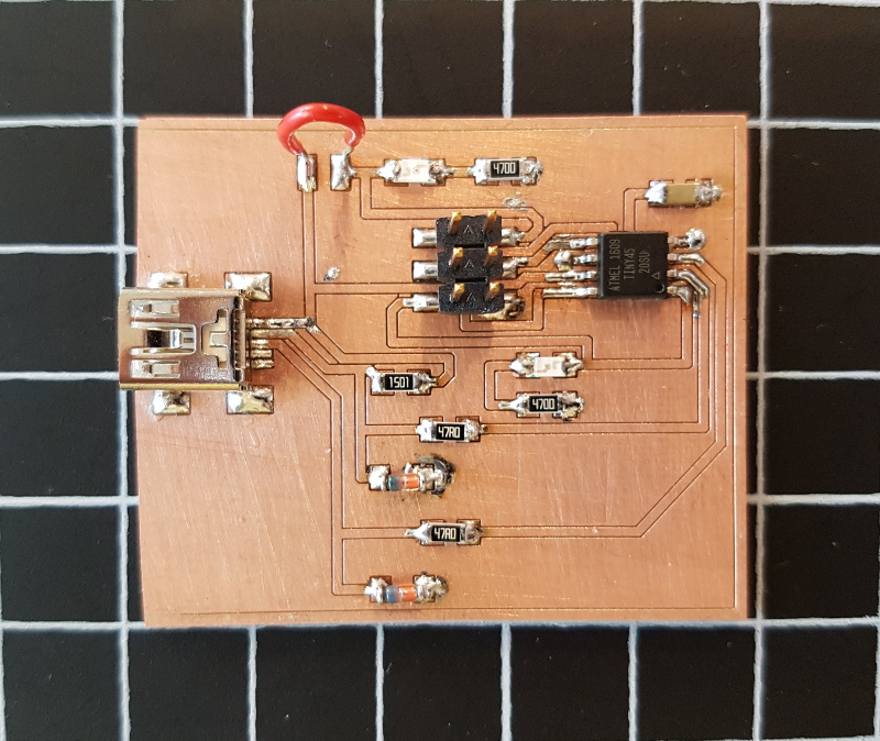 PCB
PCB PROGRAMMING
The first step is to install the software 'avrdude' in Linux
using this command line in the terminal:
→ sudo apt install avrdude gcc-avr avr-libc
Download the firmware source code and unzip it.
→ cd Downloads (cd into the source code directory)
→ unzip fts_firmware_bdm_v1.zip
More information about this: http://fab.cba.mit.edu/classes/863.16/doc/projects/
ftsmin/index.html
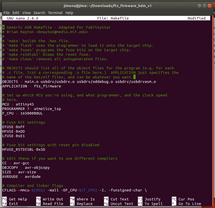
→ cd fts_firmware_bdm_v1$ make the file fts_firmware.hex is added in the directory
To check which programmer you are using in the Makefile use:
→ $ cat Makefile
To change the text use nano:
→ nano Makefile
If you are using the ATMEL ICE, it should stay (second row):
PROGRAMMER ?= atmelice_isp
- Save the nano file and close it:
→ $ Ctrl+O
→ $ Crtl+X (escape)
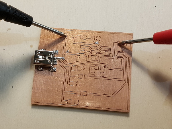
Plug the PCB into a mini USB port, the red LED should light up.
It is important that you get pin 1 in the right place. For the Atmel ICE connector I found this graphic:
To program the ATtiny45, its own flash memory with the fts_firmware.hex file:
→ $ make flash
If it doesn’t work you have to check the components, its direction and connections. Perhaps there is a shortcut.
The next step is to set the fuses that control the microcontroller. Enter this command in your terminal:
→ $ make fuses
If you see several progress bars and no errors, it has worked.
Now it is important that you check the USB functionality of your board. Unplug your board and disconnect the programmer. Now plug your board again into your computer.
NOTE: After running ‘make fuses’ in the terminal and not showing any errors, Ubuntu doesn’t find the microcontroller.
→ $ lsusb (to see all devices)
→ $ dmesg (this command provide you more information about the errors)
Response:
→ new low-speed USB device number xx using xhci_hcd
…
→ device not accepting address
→ unable to enumerate USB device (screenshot on the right).
Next week I will check this error with my instructors.
 Makefile
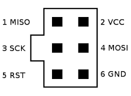 Atmel ICE Connector
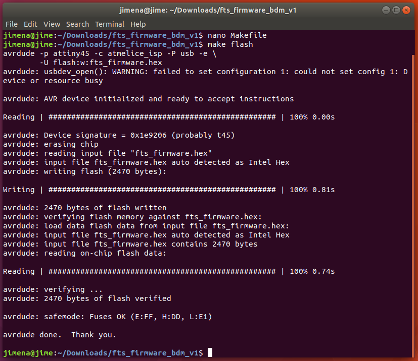 Make flash
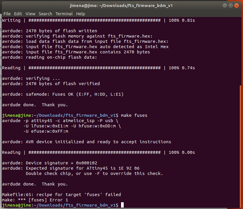 Make fuses
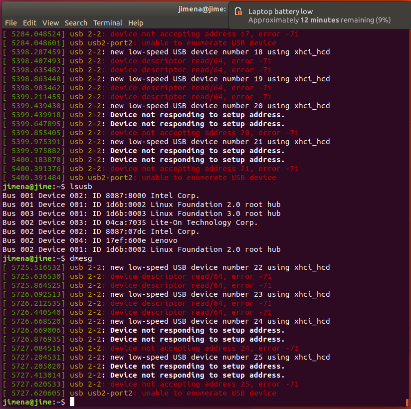 .
.Download
| EAGLE files(zip) | Download |