Week 4: Electronics Production
Assesments for this Week:1. Characterise the specifications of your PCB production process (group project)
2. Make an in-circuit programmer by milling the PCB (program it, so that you can use it to program your board in Electronics Design week, and in other weeks), then optionally, trying other processes.
Many thanks for help in this week to Tobias, Aleksandra, Florian, Marcel and Peter.
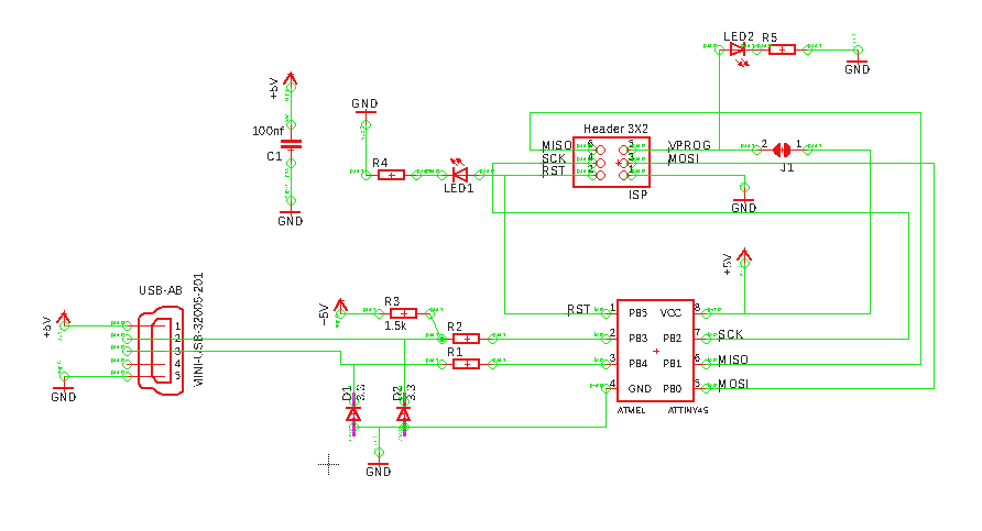
For the production of PCB board we all used the finished Eagle-schematics (see next image) that our colleague and Instructor Florian Paproth had created. He was a FabAcademy student from HRW-FabLab Bottrop in 2017.
For the download of Eagle (Autodesk) we could use our Autodesk account. There is also free version of the program for noncomertial use. The version I have used is Eagle 8.6.2 for MacOS X (64 Bit).
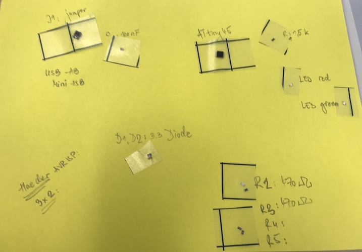
From the Eagle file you can export the BOM as a text file, which can be seen in the folowing image.
Partlist
Exported from programmer[10].brd at 21.02.18 01:27
EAGLE Version 8.6.2 Copyright (c) 1988-2018 Autodesk, Inc.
Assembly variant:
Part Value Package Library Position (inch) Orientation
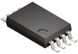
ATMEL ATTINY45 SOIC8 attiny45 (0.55 1.68696038) R0
C1 100nf C1206 rcl (0.47372293 2.16967483) R270
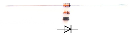
D1 3.3 MINIMELF diode (0.73017101 0.92477338) R0
D2 3.3 MINIMELF diode (0.3 0.95) R180
ISP Header 3X2 2X03_SMT pinhead+ (0.8 2.45) R270
J1 SJW jumper (0.30136565 2.3568702) R0
LED1 1206 led (0.75717594 2.16958674) R270
LED2 1206 led (0.34759264 2.59588164) R90
R1 R1206 rcl (0.66271371 1.16209646) R90
R2 R1206 rcl (0.5 1.05) R90
R3 1.5k R1206 rcl (0.30909338 1.29589985) R0
R4 R1206 rcl (0.58735273 2.16929626) R270
R5 R1206 rcl (0.46054392 2.59588164) R270
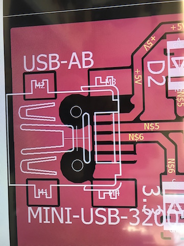
USB-AB MINI-USB-32005-201 32005-201 con-cypressindustries (0.51737143 0.62505992) R90
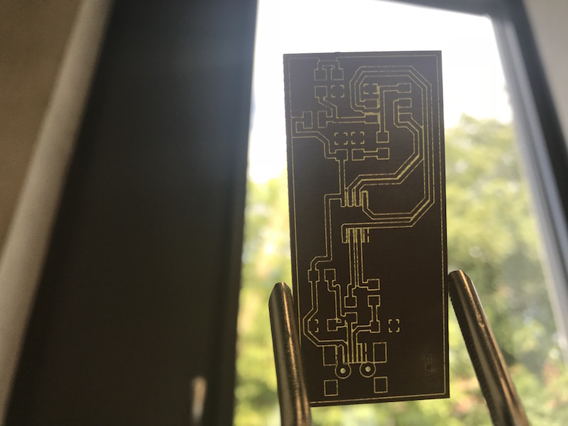
Arrangement of the Board Layout
As mentioned before Tobias our main Instructor recommended us to copy Florian's scheme and to arrange our own board layout using Eagle. For the board layout I used following tools: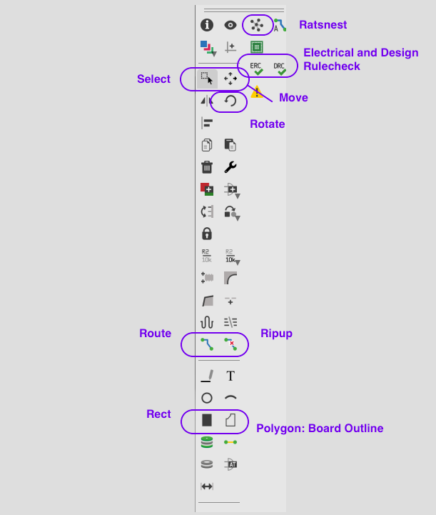
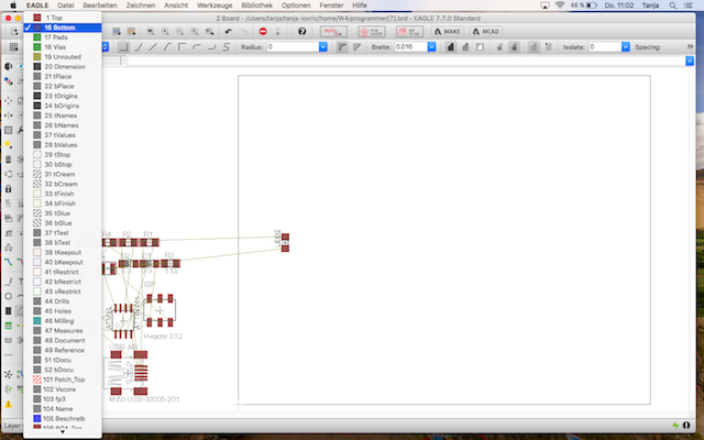
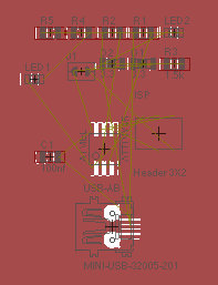
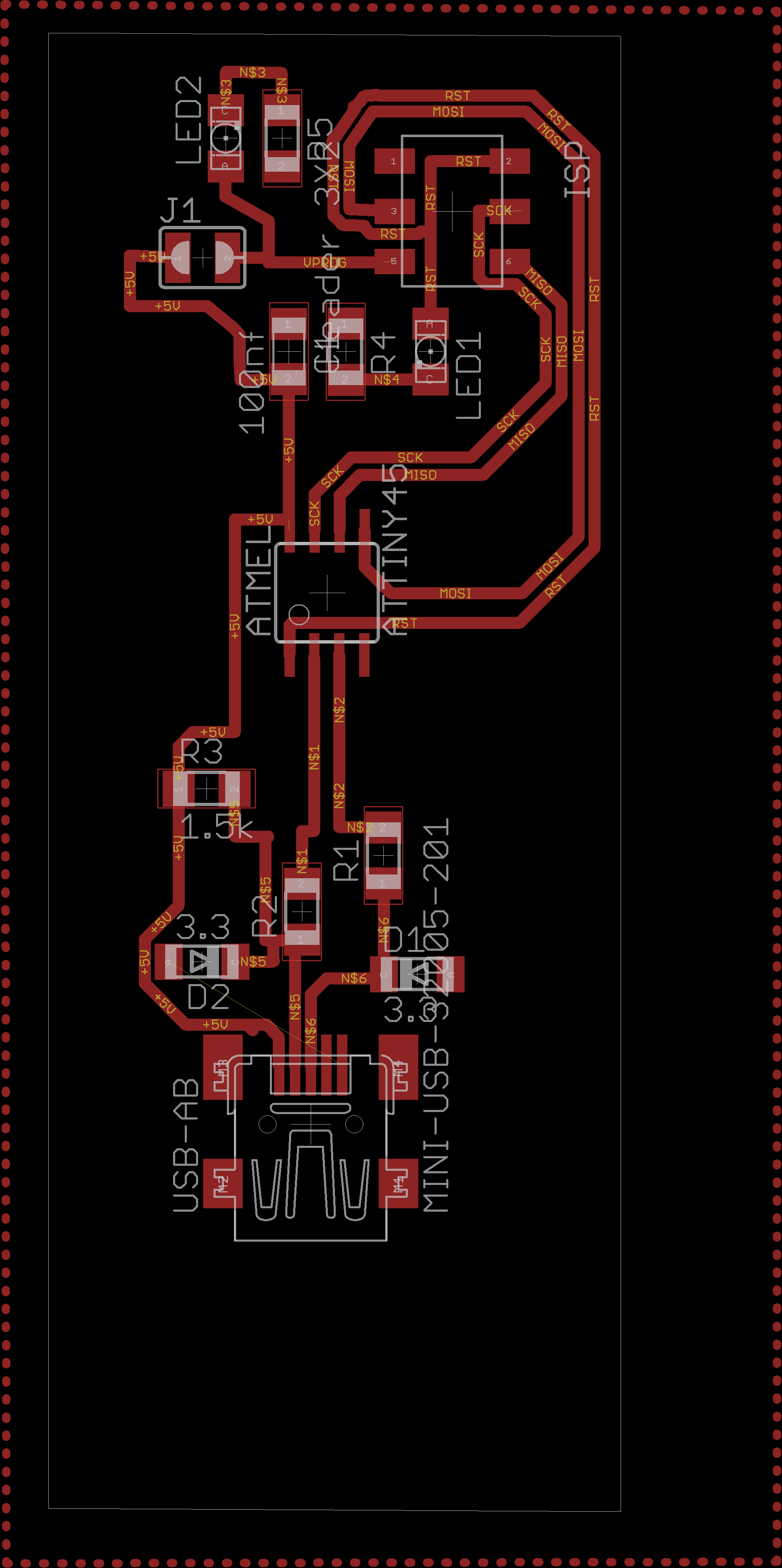
First I dragged all components into the outlined field using "move". After that there were a lot of air wires as a connection between componenets. Using "rotate" and "route" I connected and designed the layout as see below. I had to look after traces routes not to cross each other. In opposite to the scheme layout it would cause the short-circuit fault on the real board.
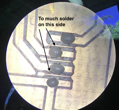
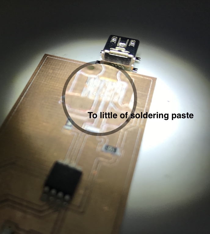
Trouble shooting
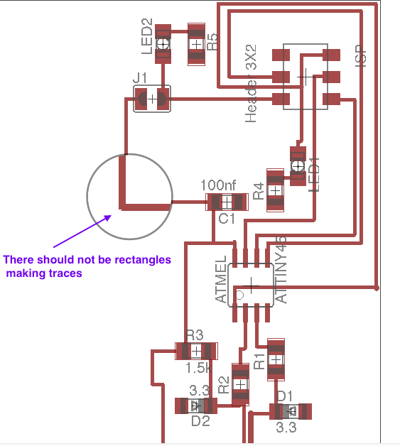
Left image: Avoid rectangle corners
Middle image: Left over air wire hard to see
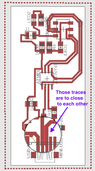
Right image: The traces are to close to each other which can cause production problems
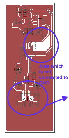
Left image: Missing GND connection in upper circle
Right image: One of the pins on the mini-USB module does not need to be soldered
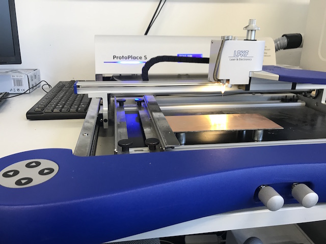
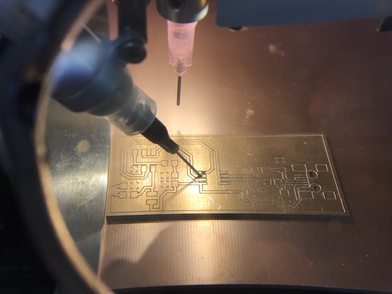
Milling and Soldering
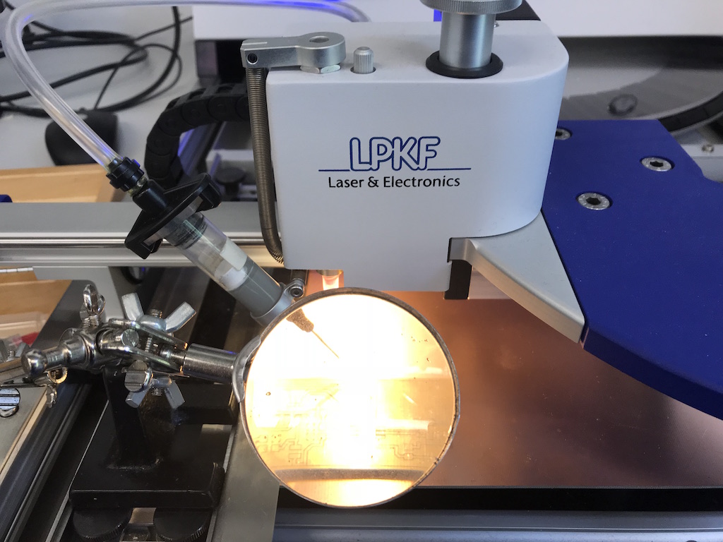
For milling we are using LPKF Protomat S63 milling machine which is very convenient to use.The perfect tutorial for using of LPKF Protomat was made my colleague Aleksandra Konopek which I appreciate very much because it was plenty of work to make it. She describes how to use the Circuit Pro system tool for rapid prototyping.
Aleksandras LPKF Milling Tutorial you can see below.
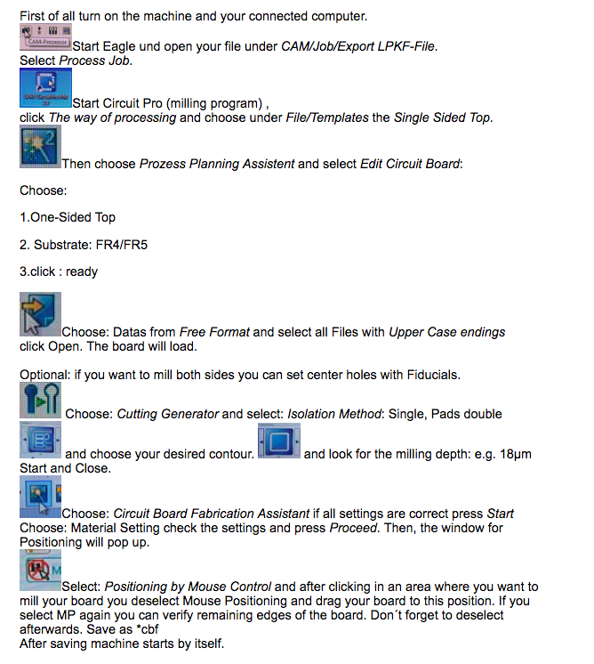
For my milling job I used Aleksandras tutorial above as a guidance.
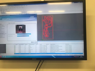
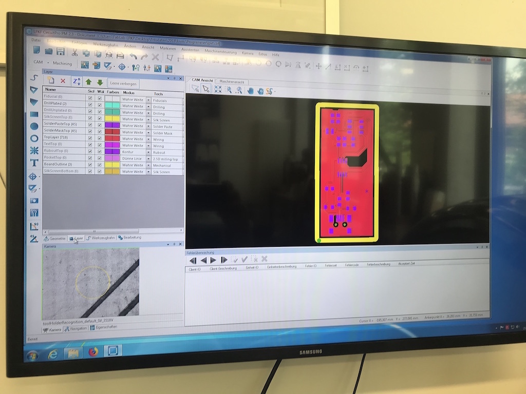
After finishing and proofing my board layout using Eagle, I saved it to an USB flash drive and loaded it on our Windows computer which is connected to the LPKF milling machine.
I started Eagle (old version) on our Windows computer and loaded my board layout file.
Then I opened the "CAM/JOB/Export" menue to generate the CAM file, which can be understand by Circuit Pro.
After starting Circuit Pro software I had to connect it to the Milling machine.
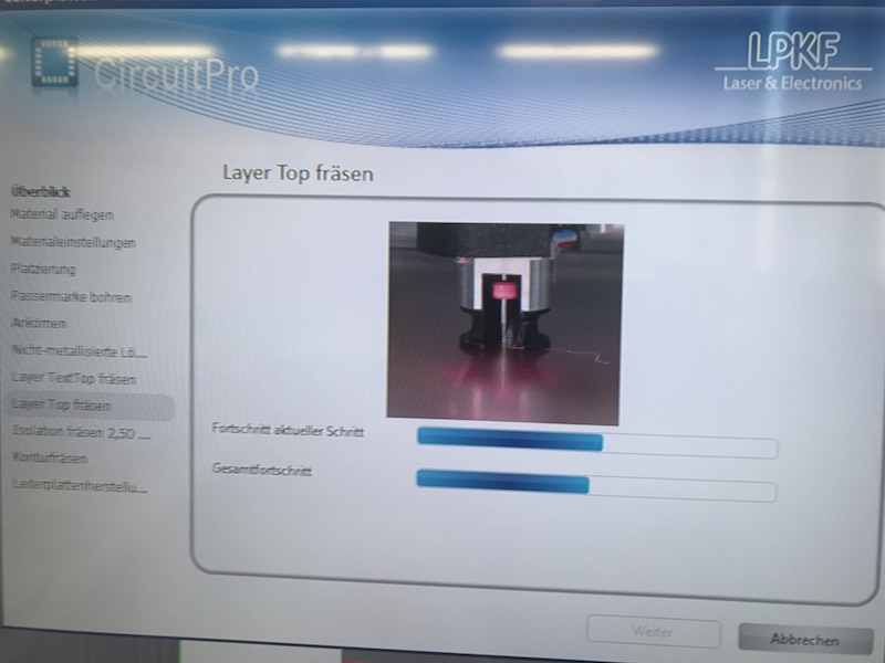
In the Circuit Pro our instructor Tobias Poppe prepared a order of helpful icons, which we should use for preparing the milling process. Those are:
Edit circuit Board (here I have choosen "one-sided Top", "FR4/FR5" as a substrate)
Then I could load the Eagle data from the CAM folder which had endings in upper case.
After that the board data of my programmer were loaded to the Circuit Pro.
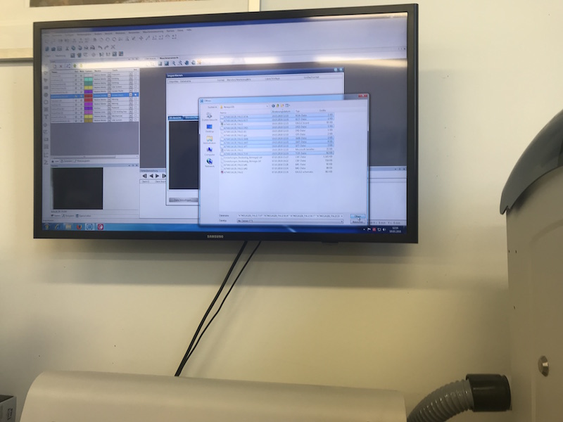
Following image shows my programmer board loaded into the Circuit Pro software of the milling machine.
Next icon was the "cutting generator" where some settings about the contour and traces should be edited.
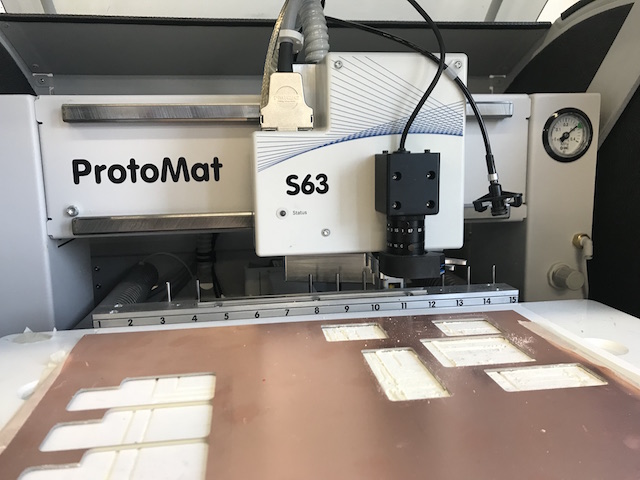
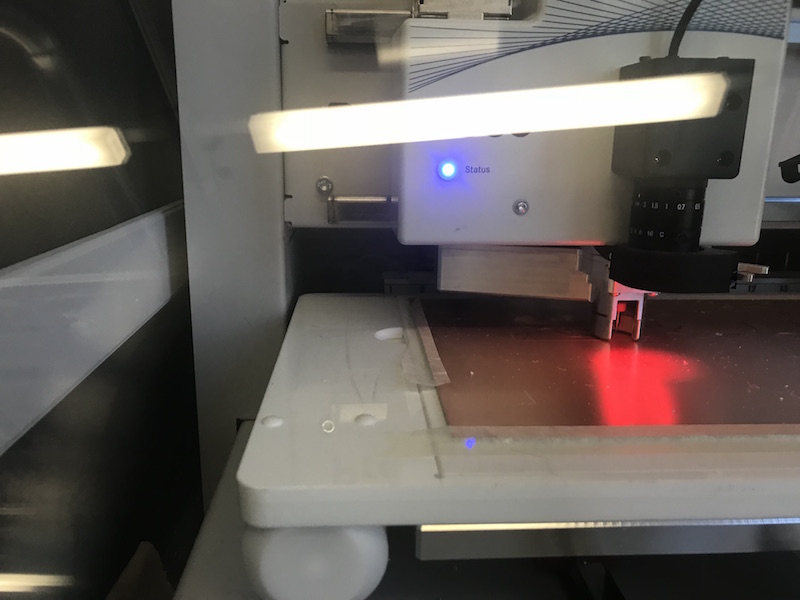
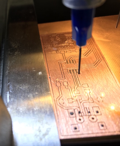
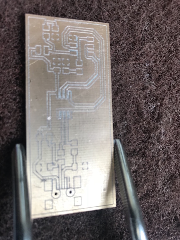
Upper image shows the milling machine just finishing the milling job of my programmer.
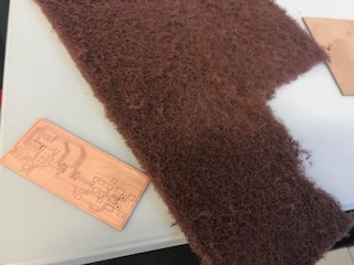
As my board was finished I hat to burnish it and to sprinkle it with the protection laquer.
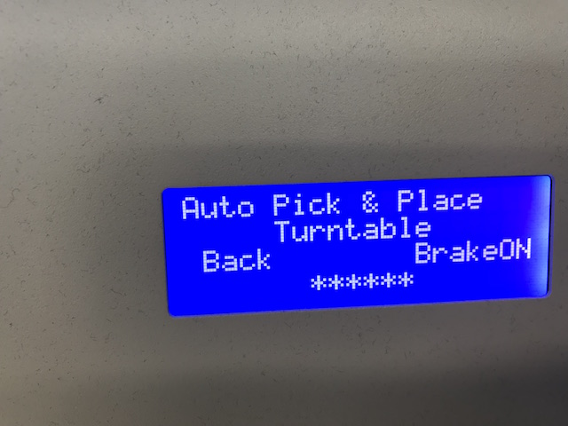
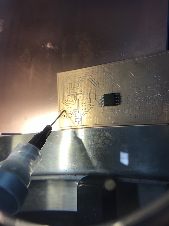
Groupassignment: Picking and placing the components
Protoplace is a semi automatic pick and place turning table. You can despence the soldering paste semi automatic. For this we use the function "Auto Pick and Place" and "Brake On" for precise positioning of the despenser.
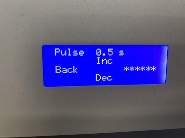
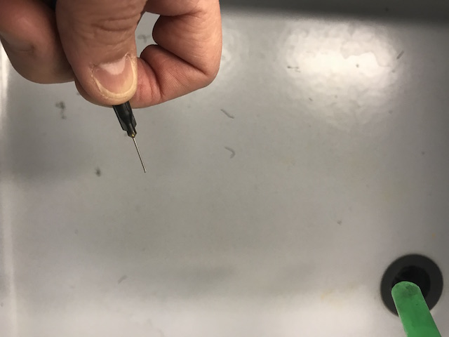
For the right amount of the soldering paste it is possible to set the dispensing time. E.g. "0.5 s" is good for bigger traces like footprints for header. For the chip footprint it is better to set the despenser to 0.3 s. You also have to take care about the size of the needle.
Dispenser above the plane board.
Now it is time to place the components. We should notice the right orientation of the MCU and the LED. MCU has an circle sign on the top. We should compare it with the pinout of the MCU to position it right. LED has a greeen point which should be oriented to the GND. Z-Diode has a mark which should be oriented to the signal trace. Resistors and capacitors have no certain orientation.
AtTiny45 Pinout, but notice that the real MCU has the sign on the corner.
After finishing the picking and placing you should always clean the despenser needles using compressed air.
Soldering and making corrections
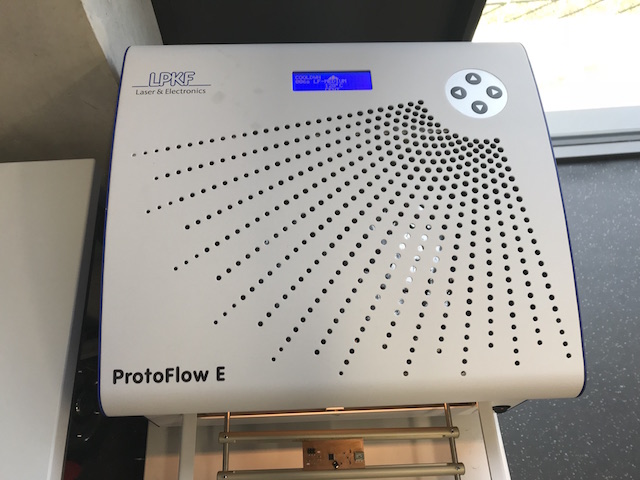
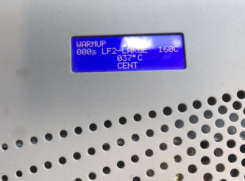
Now you can put your board into the LPKF ProtoFlow E oven and choose the setting "large" for heating temperature profile. As I have used "medium" setting some parts were not soldered properly. If they do not look shiny after burning process they were not burnt long enough. According to this the connections will not be stable.
Manual soldering
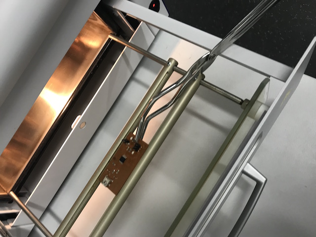
As the jumper can not be burnt in the oven, it had to be soldered manually
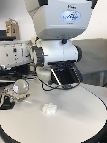
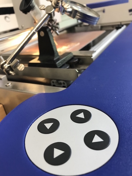
The Lynx Dynascope is a stereo microscope with 3d perception of the board. It has a 3.5x - 120x stereo zoom magnification range which allows us very comfortable working with the PCB.
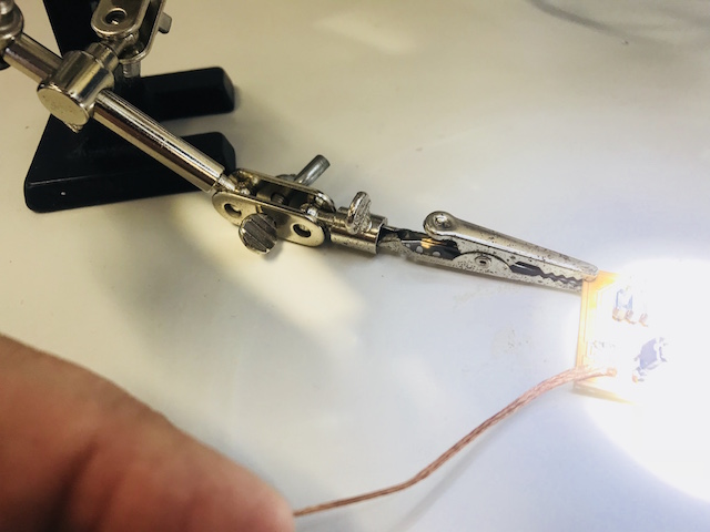
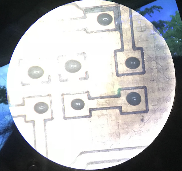
Troubleshooting: Broken connection has to be repared with the cupper wire.
Programming the Board
For programming I needed the firmware which I loaded here.Kreatives Chaos is the site on which I found the pin assignement on the 6-pole Header.
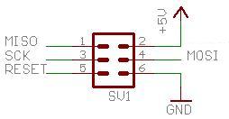
For the connection between Programmer (AVR ISP) and my programmer board it is important to know where the pins are placed.
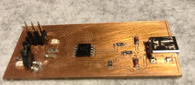
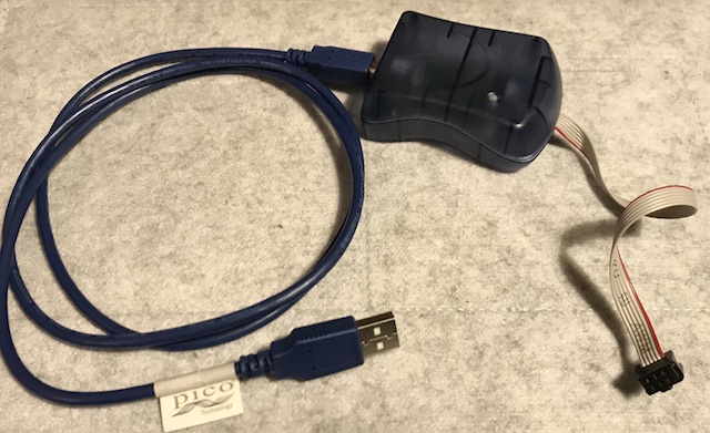
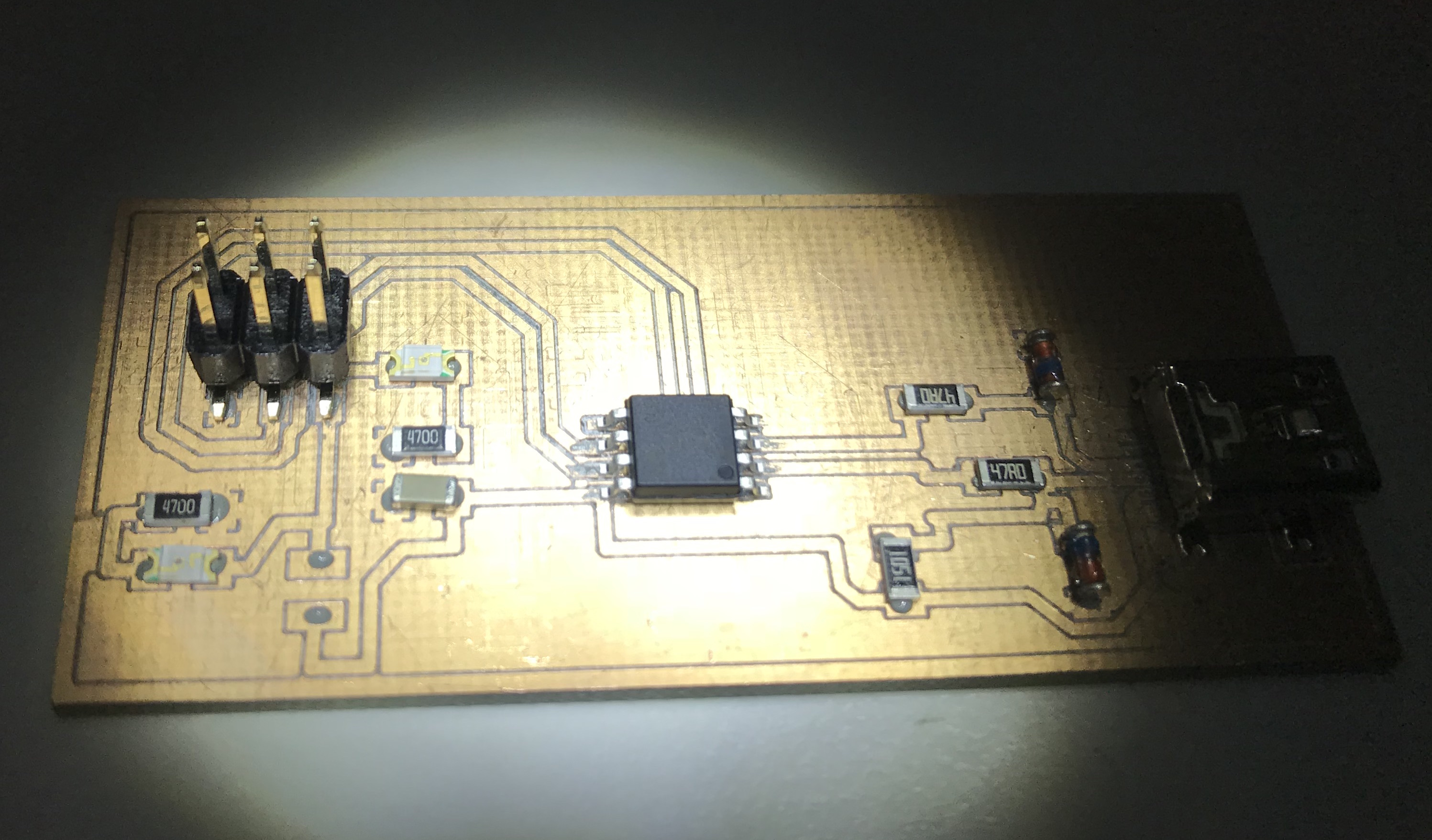
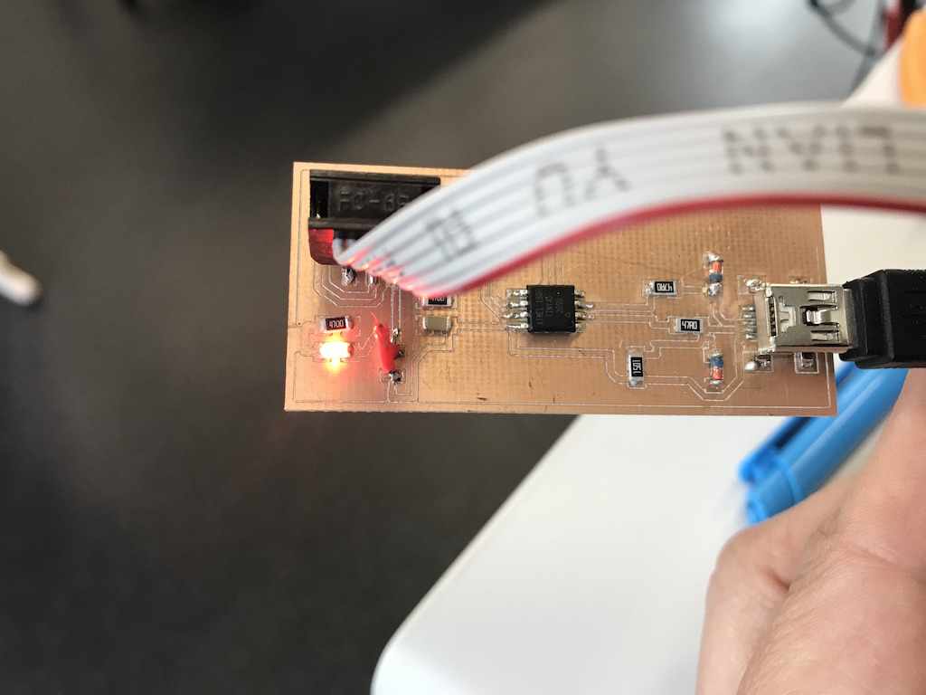
The left image above shows my finished programmer board. The right image shows the Atmel AVR ISP Programmer which I used for programming my programmer board.
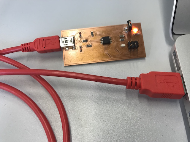
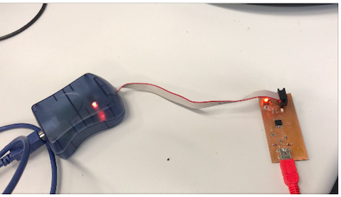
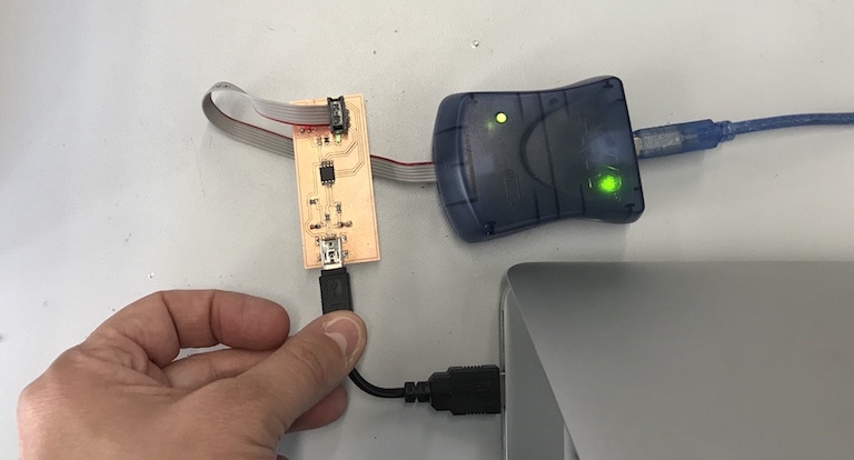
Upper left image shows my programmer connected with my MacBookAir and red LED which is switched on signaling the funcionality of power supply. The righ image shows the connection between the AVR ISP Programmer and my board.
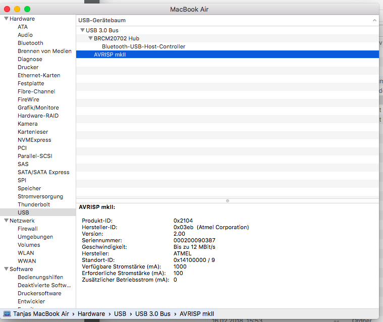
Some computers do not recognize the Programmer Boards. My MacBook Air did recognize the AVR ISP Programmer as to see above.
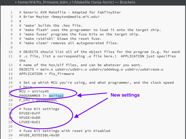
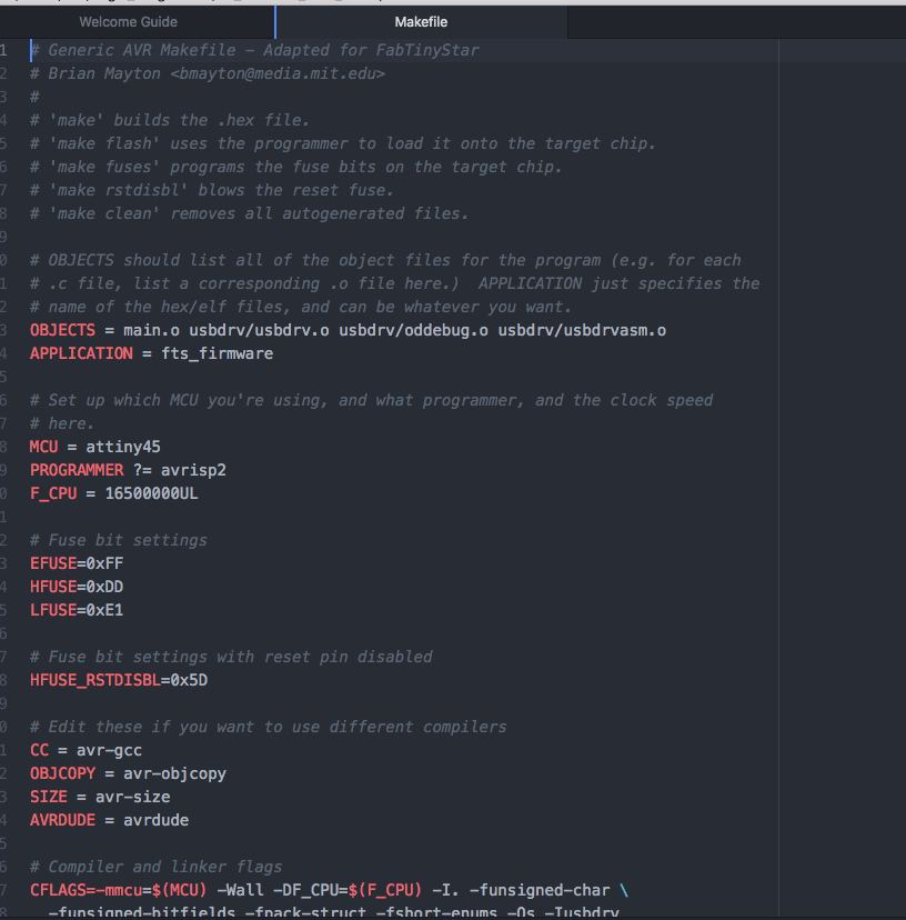
I download the firmware for using the Programmer and to changed to this folder using terminal. Now I had to make some changes in the Makefile. I changed the name of the board, fuses and the name of the programmer.
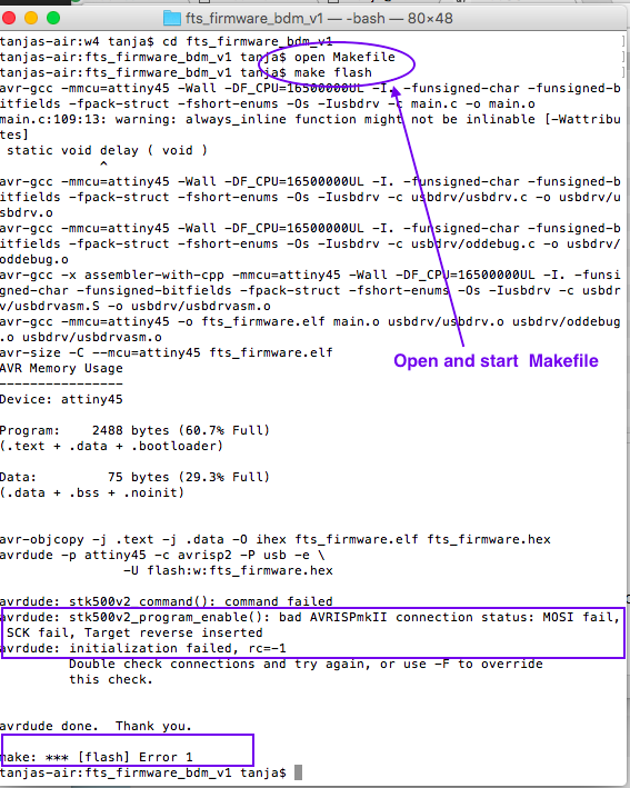
Now I could open the Makefile and start the program using commands "open Makefile" and "make flush". First it seemed to work, but then I got an error message. I checked all connections using multimeter but found nothing wrong.
My instructors and another electrical engineer tried to find out the reason for the error, but could not localized the problem. So I decided to make a new one.
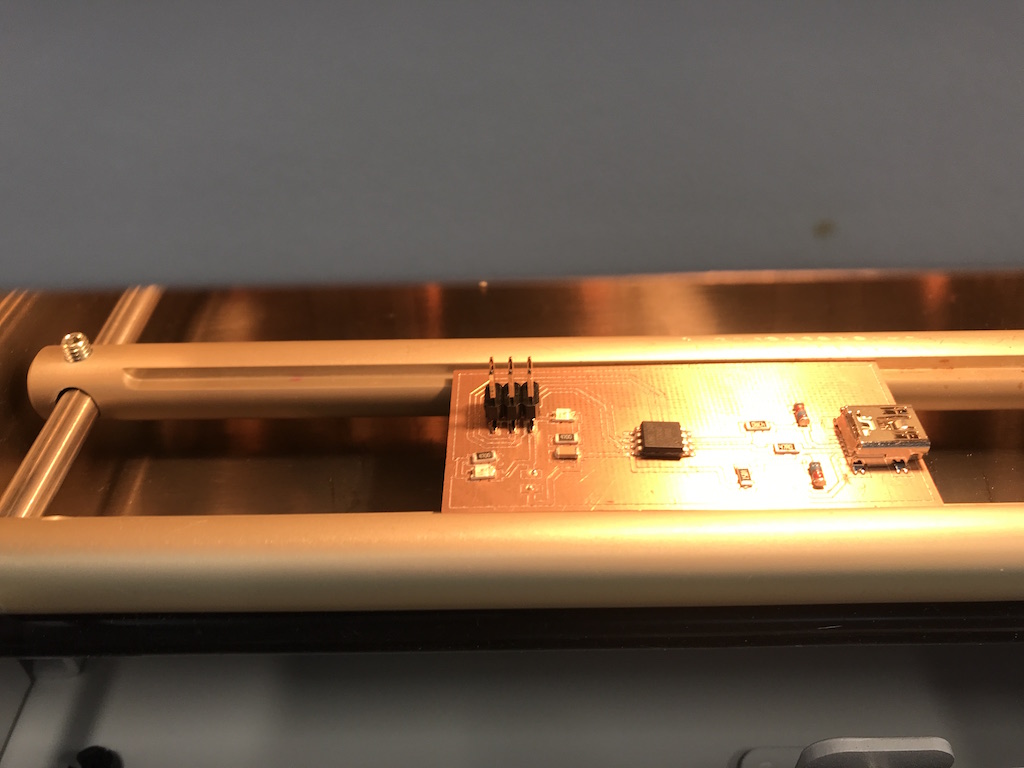
My New Programmer
For my new programmer I used the same board layout as I supposed that the reason for the mistake was my soldering. One air wire which you can see was not there in the final version of the layout.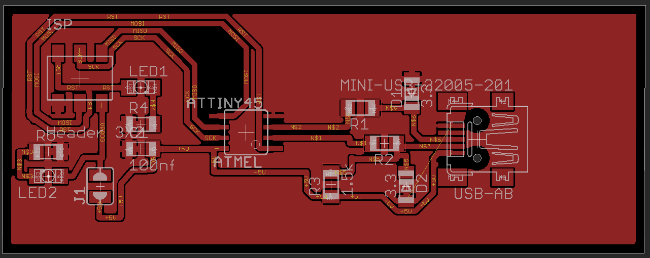
As we use FR4 in our Lab, exaustion starts automaticly with the milling job because of glass fiber particals dust:
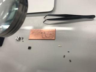
I can recomend to use adhesive tape to collect all parts you well need for soldering and to write on the paper which resistor or LED you use. On my List there is a mistake about resisotors: R1 and R2 = 47 Ohm (needed for USB) and R4 and R5 should be 470 Ohm (needed for LEDs). Many usefull tips I became from Christoph Niess who took a time for my obsacles even if he had lot to do. Thank you so much Christoph!
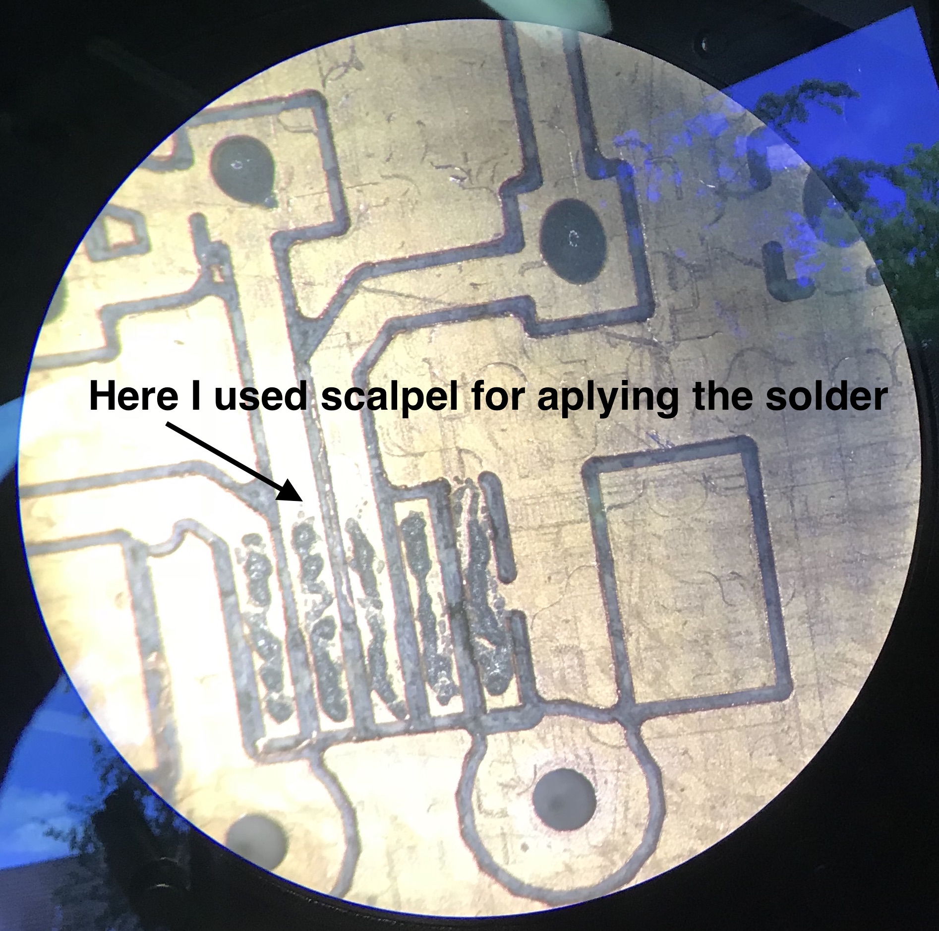
At the beginning I used the soldering pick and place LPKF machine. But the applicator diameter we had was a bit to big. So I switched to the technic I have learned by Daniel Bruns. He uses scalpel for application of the solder compound. For some parts it was still easier to use the LPKF Proto place aplicator, but for smal narrow traces such as chip or mini usb I would recomend to use scalpel.
I wanted to show how it looks like after dropping the soldering compound on the certain poits of the PCB. The solder has a strong surface tension which helps to hold one big drop of tin solder. It is made out of many small tin globulis which looks like a foam.
I made another mistake, as I put the board into the soldering oven. As I pushed the door to close it, there was a short flip there. I suppose that this was also the reason for not such good result. After the heating process in the soldering oven, usb and the chip were not soldered properly. So I soldered those parts again with a bit more of solder.
Even if I used the "Large" programm for heating and cooling process the solder was not shiny after that. But it still worked.
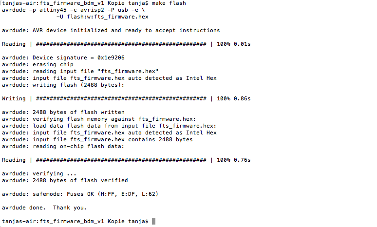
Finaly I could connect my new programmer to my computer and program it using AVR ISP programmer.
I am so happy to have finaly a working programmer. Now I cann programm other boards using my own programmer! :))
Downloads
|
Download crosspack
Zaerc's FabTinyStar page download Programmer board and scheme (zip) |