Week 7 - Electronics design
Group assignment assignment
use the test equipment in your lab to observe the operation of a microcontroller circuit board. This includes oscilliscope (look at the signals), signal generator (), multimeter (measure voltages to check that the supply voltage is correct), bench power supply (to set the voltage and then dial up the current).
Here is a link to our lab's page which includes links to all our group assignments.
Assignment summary
what I achieved/learned this week:
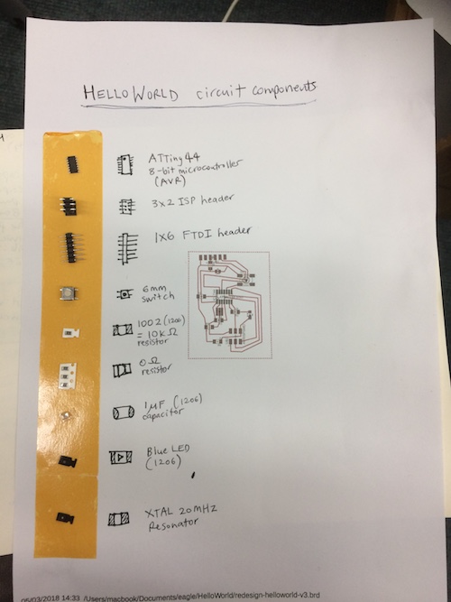
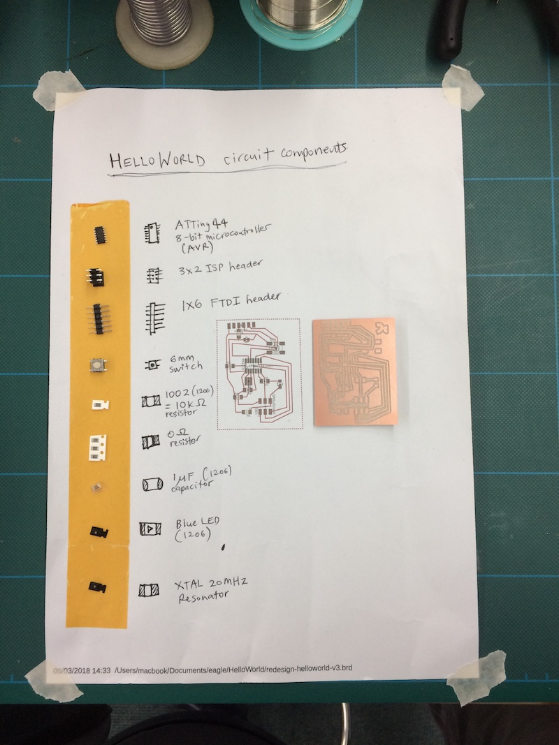
- designed the echo hello-world PCB in Eagle software with button, LED and resistor
- brought the .png files into photoshop to add logos
- generage g-codes using fabmodules.org
- setup the machine and CNC milled my board
- stuffed my board with all components
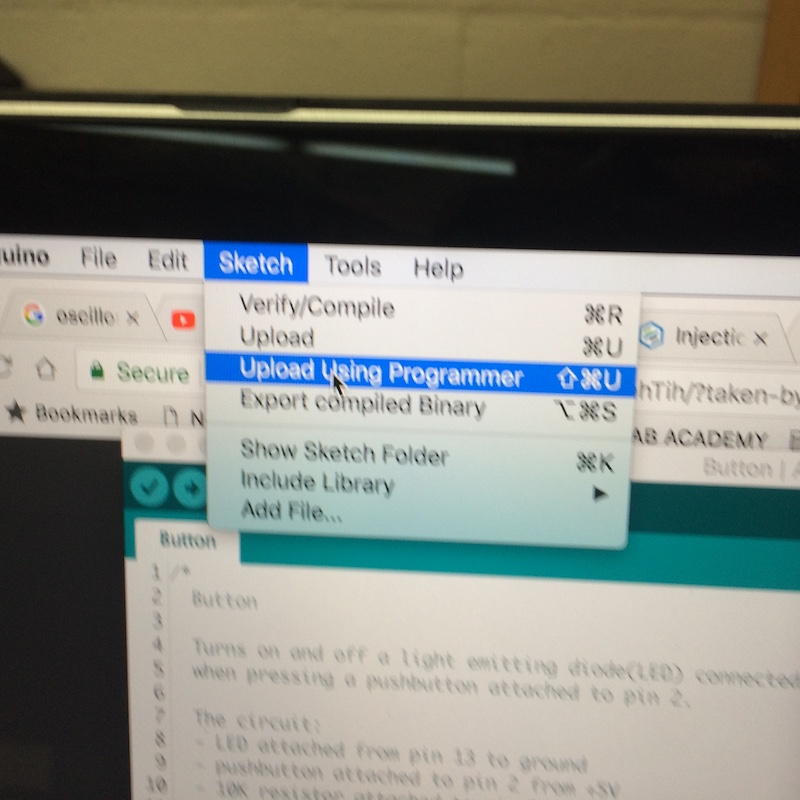
- programmed my board using my ISP programmer
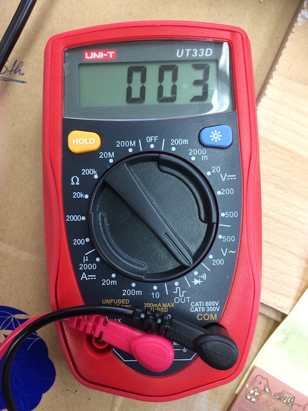
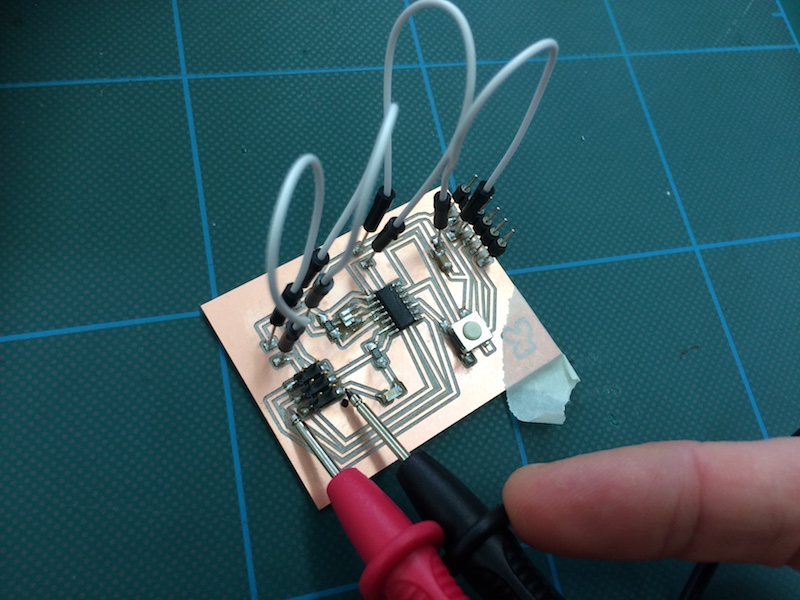
- debug/tested the board using the multimeter and oscilliscope
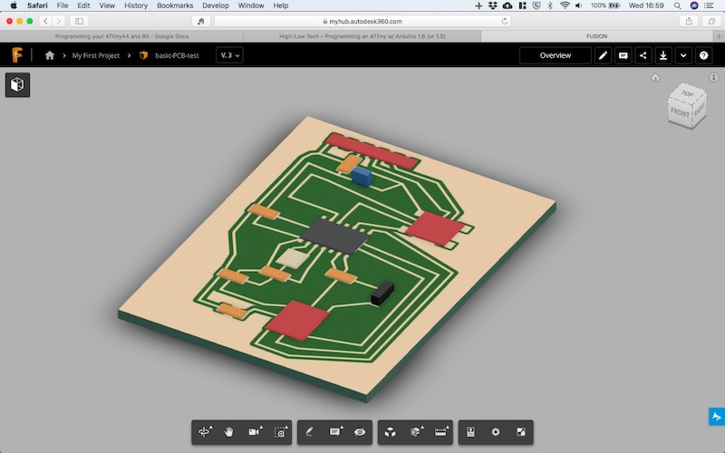
- created CAD model of my board using the associative link between Eagle and Fusion 360
Individual assignment for this week
redraw the echo hello-world board, add (at least) a button and LED (with current-limiting resistor) check the design rules, make it, and test it. Extra credit: simulate its operation extra credit: render it
To summarise the key aspects of electronics design I found:
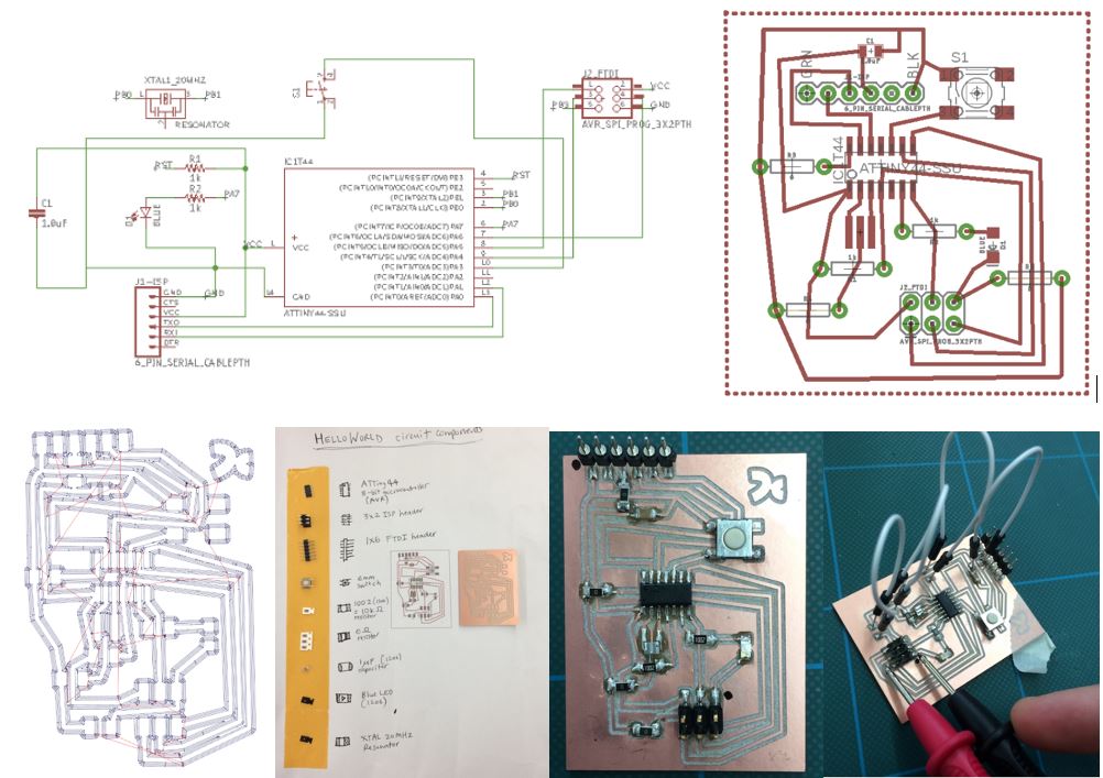
- adding buttons: connect a resistor (in the order of 10kOhm) between the button and VCC. This is a pull-up resistor which stops a short when the button is pressed. The button is connected to a digital PIN
- adding LEDs: add a resistor in series with the LED. This creates a voltage divider circuit, which specifies a correct voltage (called the forward voltage, Vf) to be lost across the LED. This is typically 1.8V. LEDs can be connected to a digital pin (specified then as HIGH/LOW in the code), or an analogue pin (specified as a number between 0 and 1023 (10 bit) that is proportional to the amount of voltage being applied to the pin.
- pull-down resistors are used if you want the default to be HIGH/ON (note both pull up-down resistors are used also with PNP and NPN transistors with opposite effect
- capacitors (used close to the microcontroller or crystals) are used as decoupling capacitors (to supress high-frequency noise in power supply signals), power supply filtering (to help convert AC to DC - used with diode rectifiers), energy storage and supply (for quick energy delivery), and signal filtering (they can block out low-frequency or DC signal-components) - make sure to design your circuits with capacitors that have a much higher tolerance than the potentially highest voltage spike in your system. A good
- external crytals/resonators are used if you need something more stable than the internal oscillator that is built into the microcontroller. They can also be used when you want an exact clock speed at a different frequency to the internal oscillator
It is worth showing this up front. I found this sparkfun page on pull-up resistors to be incredibly helpful. It took me a while to get my head around these, but this page explains everything very well including what they do, how they work and how to calculate their values. The take home messages are:
- pull-up resistors (pulling to Vcc) are more common that pull down (to ground)
- typically they are in the order of 10kOhms
- they are used to stop a short between Vcc and GND when the button is pushed. The default here is OFF.
- the value of resistor controls how much current you want to flow from VCC, through the button (when pressed), and then to ground. The pull-up resistor also controls the voltage on the input pin (it needs to be close to Vcc), when the button is NOT pressed
- you can enable an internal pull-up resitor with the following code:
pinMode(5, INPUT_PULLUP); // Enable internal pull-up resistor on pin 5
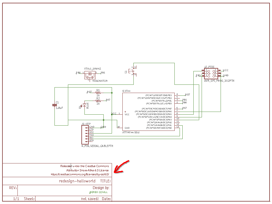
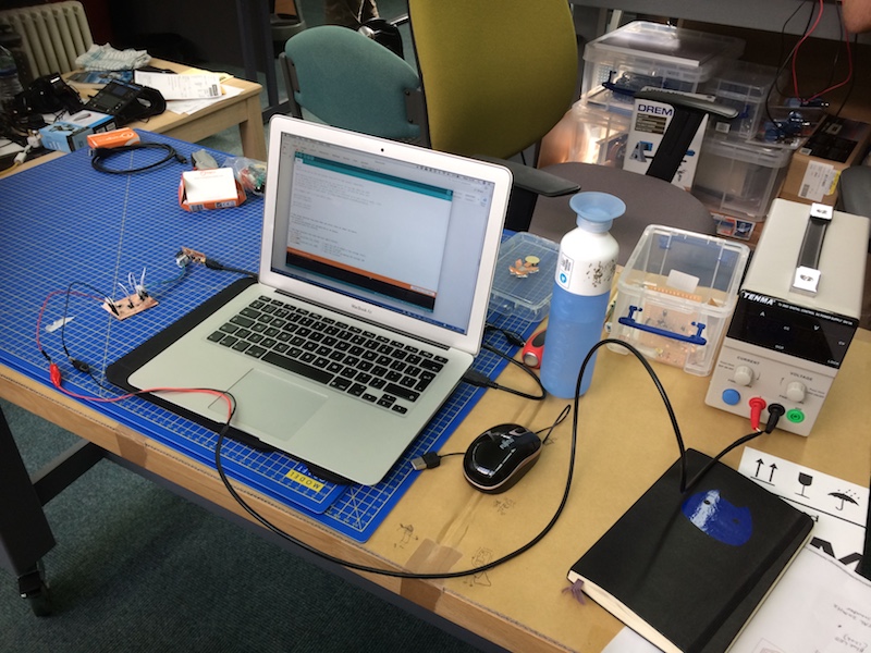
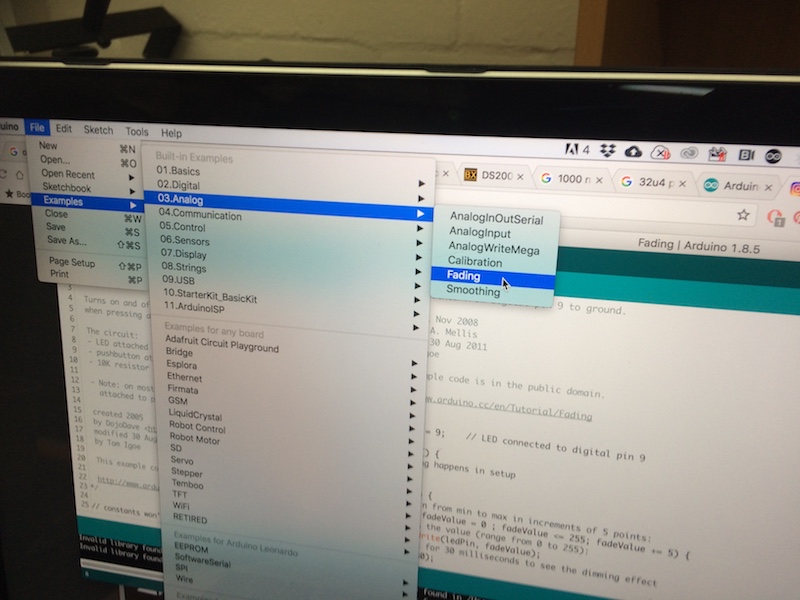
I used Eagle to design my circuit (free download here, and after some initial frustrations found it to be ok, although to some extent I was flying blind, at each step not really knowing about the next. I found the tutorials by Sparkfun to be quite good in general - both for creating the schematic in Eagle, and for creating the board layout to be milled> but also for using test equipment (multimeters, power supplies, oscilliscopes, signal generators). They may not be the best, but their quick, consistent format makes for easy digestion. These videos are embedded a bit further below for reference.
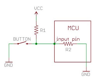
Anyways, here is the original trace that we needed to create.
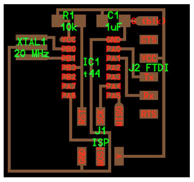
and here's how these pins relate to the Attiny chips.
and here are the original components on Neil's board.
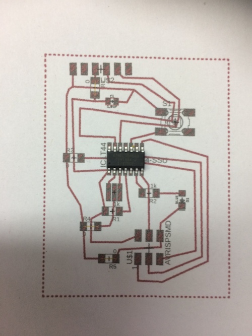
Here is my early schematic in a Frame. There were a few problems with this. The connections at the C1 were not quite right, so I had to redo these. I found this out in the traces diagram where there were no connections! Also, I got the naming for J1 and J2 around the wrong way, so I needed to rename these. Also there was a connection missing from the J2, so I needed to redo that.
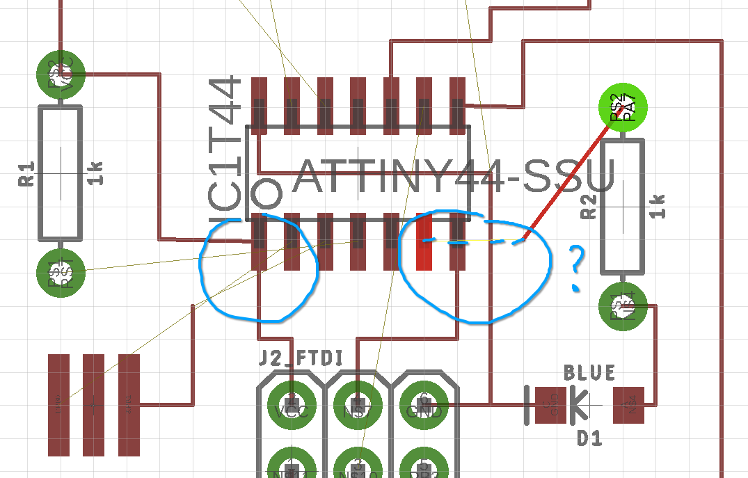
I struggled early to get the traces not to cross. In the end, I used a few 0 Ohm resistors, but that felt like cheating. I realise that you can use boards with multiple layers, but I didn't want to do that in the first instance.
I also used the default 10mil trace width which really is very small, so I updated these to 16mil all round. Here's the early crossover challenges shown with the old trace width (10mil).
I used resistors that were too big, so I need to update these. Here's the original traces diagram with the polygon border which I then used to create 'copper ground pour' to fill the board with copper so it won't be milled later on.
Here is the board with the copper fill too.
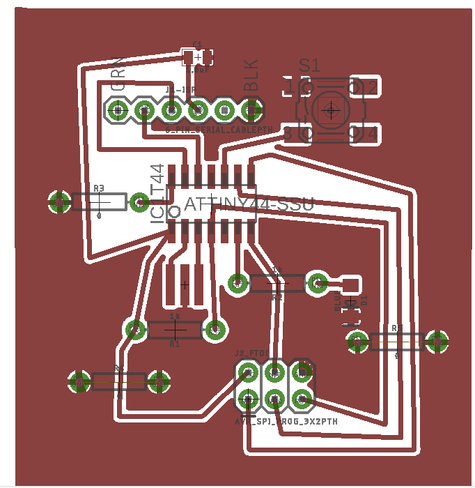
Then I adjusted the schematic to include some 0 Ohm resistors. I wasn't sure if the tracks would fit underneath the connectors, so I thought using 0 Ohm resistors was the best option.
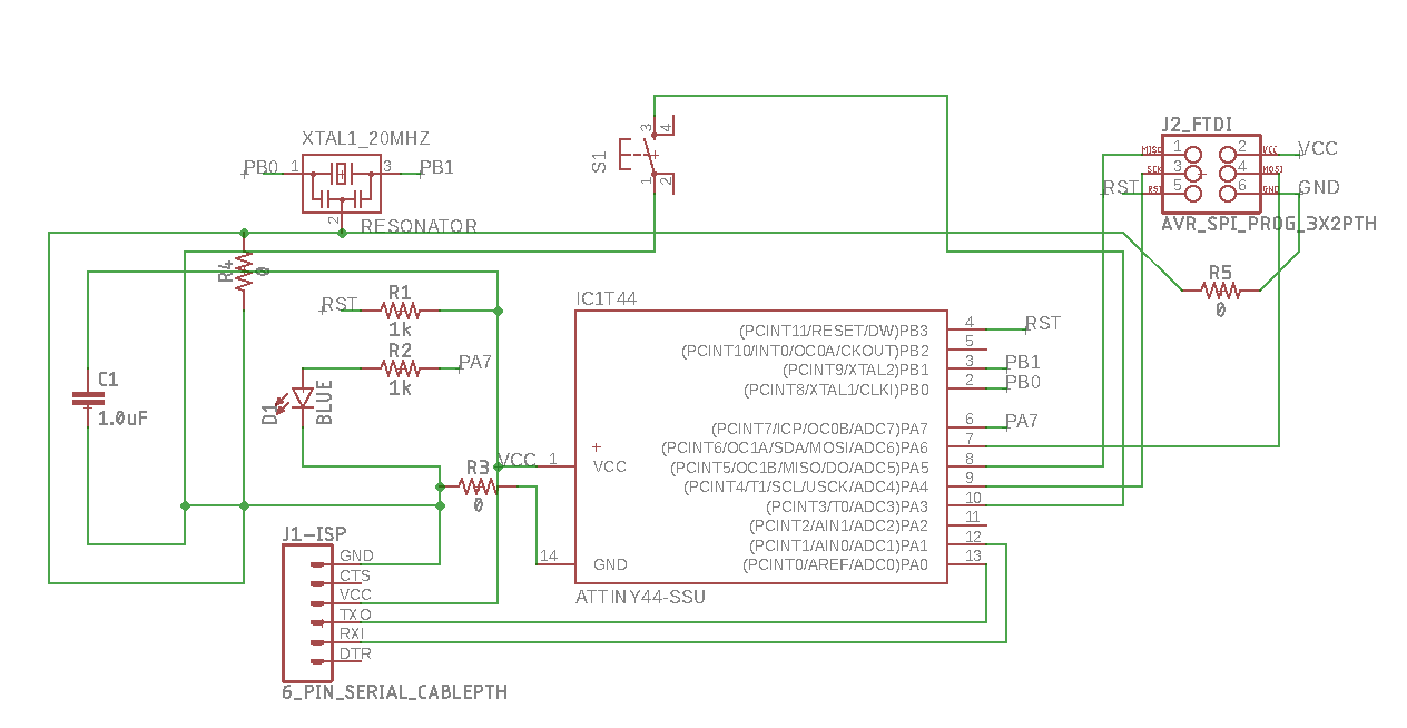
Then I found out that some of the components that I had selected from the library wen't compatible - then I actually found out about the fab library which was quite frustrating. I had to redo quite a few connections and this took a bit of time. Anyway, here's the updated schematic.
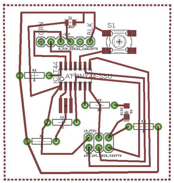
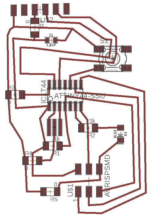
And the updated board design.
Then I heard that printing a paper version of the PCB was a good idea to check that the scale was right using the chip to check. Here's the printout..it looks so small in real life!
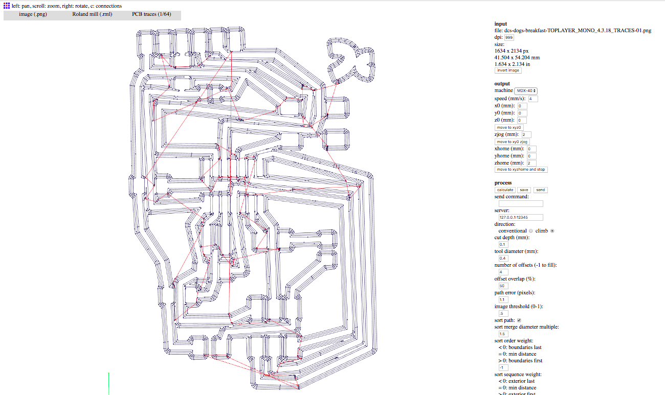
Then I transferred the high res png file (1000 dpi) to Illustrator, using the EXPORT option as PNG, and making sure the MONOCHROME option was checked. Before I exported the image, I also turned off the display of the pad/signal names (options/misc). Then I cropped it in Illustrator, checked the size (sometimes the sizes aren't right), then I made an outline on a different layer and saved out the two layers (outline.png and outline.png - as outlined in our group milling tutorial. Then I uploaded the traces.png file to fabmodules.org and milled the board (making sure the scale was right and the image was inverted). Then I uploaded the outline.png and milled this (making sure I changed the tool diameter to 1mm).
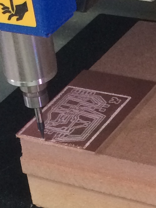
Here's the board milling, it didn't take too long, perhaps 5 minutes?
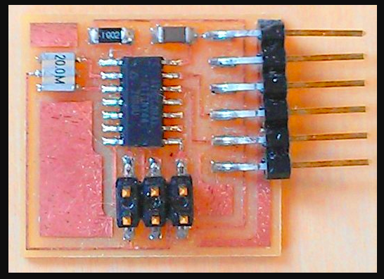
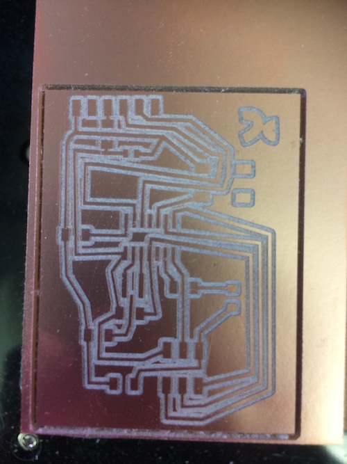
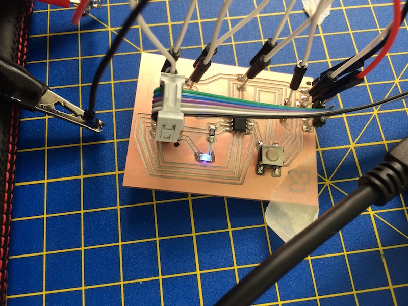
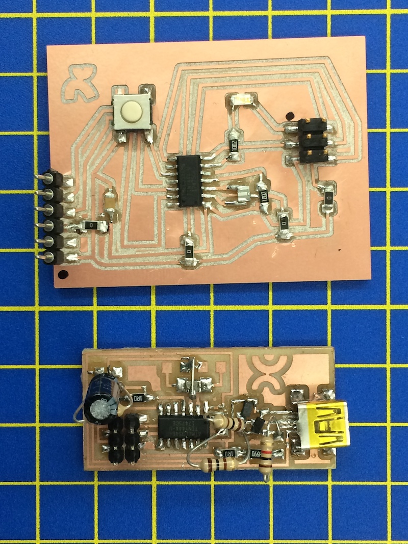
Here's the board as milled. It came out quite nicely, although there are some slivers that I'd like to design out in the next iteration.
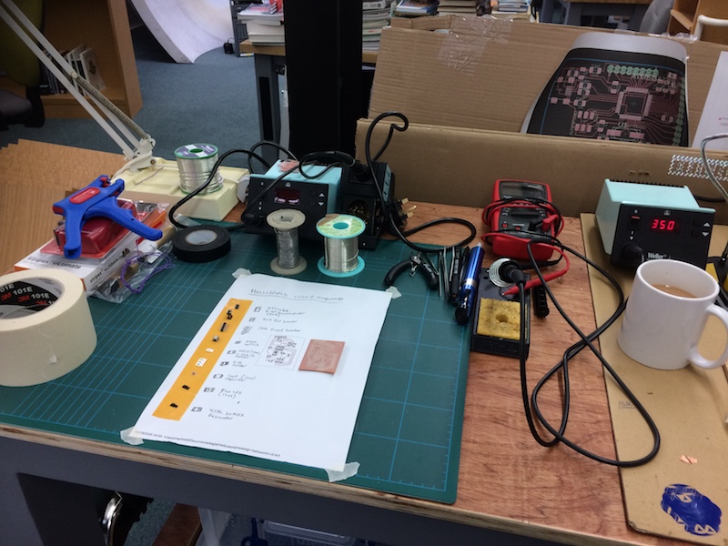
I am trying to be more organised with my soldering this time, so here are all the parts laid out ready to go. I need to check though, I think the 0 Ohm resistors in the lab 1R0 are actually 1Ohm resistors...I wonder if that is sufficiently low to be acceptable?
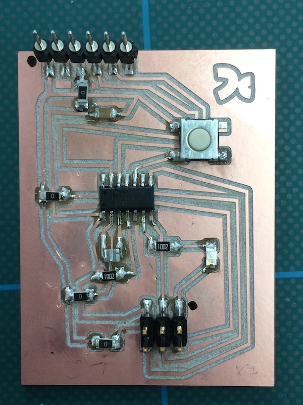
Ok, so ready to solder everything up.
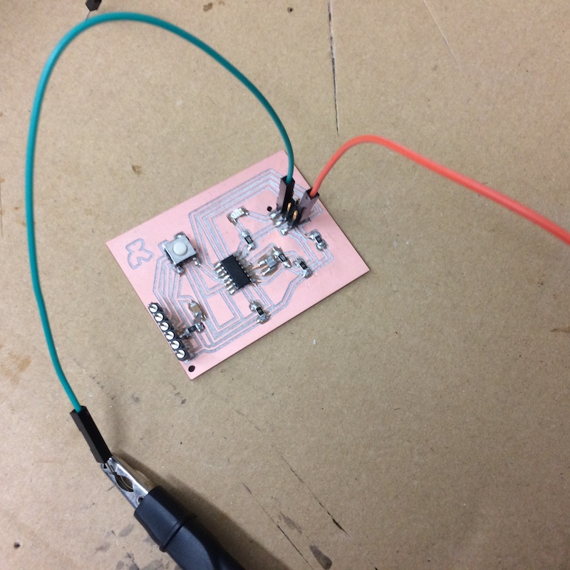
and here it is soldered and ready to go! I used these white jumper leads as we only had 1R0 resistors, not real 0 Ohm resistors, so I thought I'd use these just in case and test them then do some calculations to see if the system would be sensitive enough to deal with the 1 Ohm resistor...that can come later.
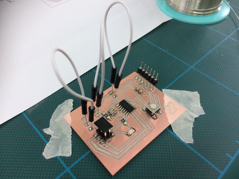
so then I installed the arduino IDE and the library for the ATTiny boards. Then, allocating the board, processor and programmer to the correct chips (all in TOOLS menu), I then did BURN BOOTLEGGER to get things happening. It was a dissappointing end...there were errors.
So doing some debugging with Luiz, we realised that one of my 0 Ohm links wasn't there... I'd completely missed it! I had also connected the J1 ISP the wrong way on the programmer board. After connecting the last 0 ohm, it worked! Oh so happy!!!!
Then after redoing the 0 ohm resistors (doing them properly this time)
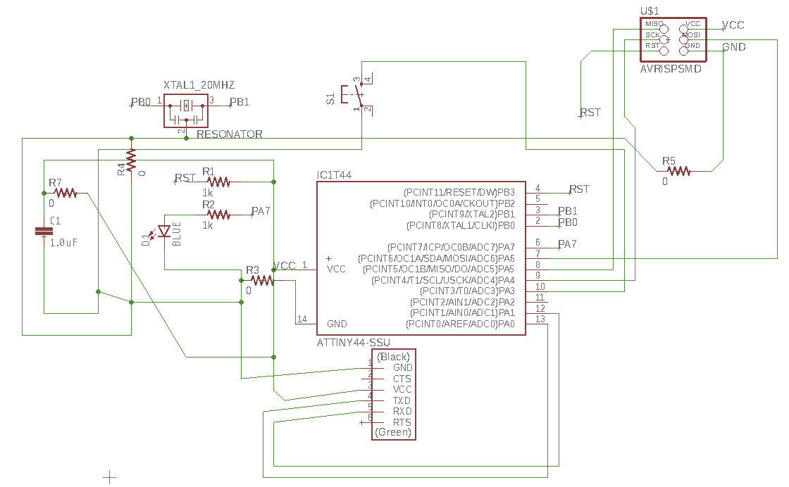
I managed to then integrate the PCB design in Eagle with a basic part in Fusion. First I checked the rectangular dimensions of the board I created in Illustrator in order to create the correct size envelope. I used a good tutorial to take me through step by step, here tis:
Latest files to download
Still some things to do though:
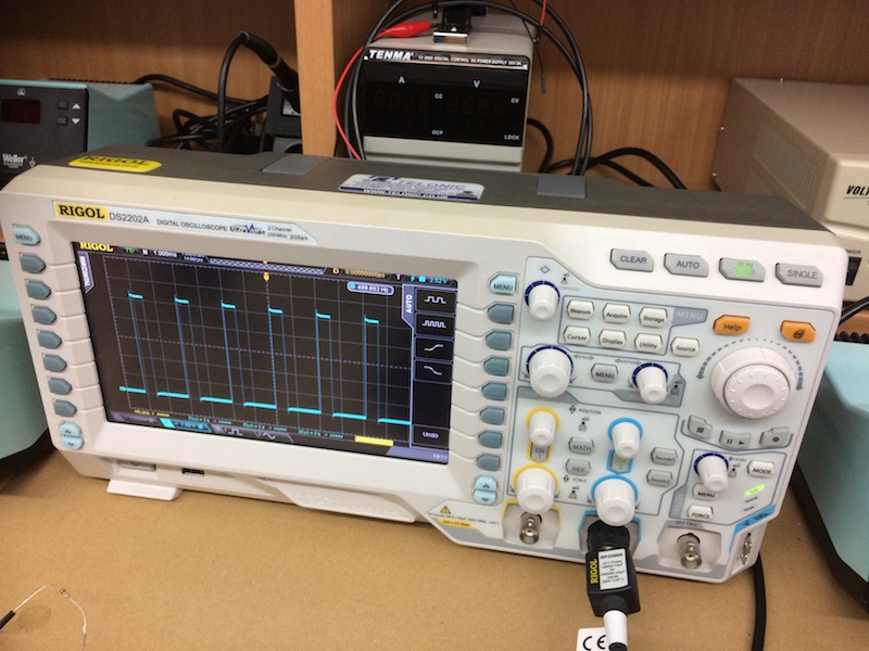
- use the osciloscope to analyse if there is any noise in our board
- to simulate what happens, and document what's happening in this circuit. For instance I used a 10k instead of a 1k resistor. This made the LED quite dull.
- document the learning that took place with out mentor. I learned a lot during a short tutorial session, and I want to make sure I capture this and build upon it here in my documentation.
- to try to fix my original programmer, and use this to program my board!
- try to synchronise Fusion with Eagle, and Solidworks with Circuits plugin. Here's a good example how to link Fusion/Eagle . Also, here's a tutorial that I used to sync the two: https://www.autodesk.com/products/eagle/blog/fusion-360-integration-eagle/
Here are those handy videos from Sparkfun I mentioned earlier. How to use a...
Multimeter
Benchtop power supply
Oscilloscope
Function or Signal generator
I did quite a bit of work to produce our group page showing how to generate the HelloWorld board in Eagle.
Here is a link to our lab's page which includes links to all our group assignments.
NOTES FOR MYSELF TO TIDY UP later... a good example watch video again!! describe what the components do and what they're used for (and symbol...USE EXAMPLE BASIC CIRCUITS TO DESCRIBE WHAT THE COMPONENTS ARE DOING: resistors: limit the flow of current. They are used to protect the circuit from high currents, e.g. current limiting resistor is a term often used. voltage: difference in potential. Analogies include capacitor: inductor: crystal resonator diode zener diode LED can blow LED with power supply (ie not with small battery with high internal resistance, but not with good power supply) transistor bipolar vs mosfets Mosfets are good up to a few hundred volts: we use these to switch power. note: RDS (resistance between drain and source), you want this to be very low. op amps: analogue amplifiers, used to amplify voltage or current or to filter. Microcontrollers now have that capacity built into them. Microcontrollers: 1. draw a schematic circuit to define what components are needed and how they are connected. Note that I will need a library of the parts before I get started. 2. draw position where they go on the board 3. route how the traces make the connections (can be done by hand or automatically called autorouting) 4. fabricate it on the mill design rules: - how skinny traces can be - how close they can be - number of layers needed the header is where we load the programme. capacitor is filter to clean up the power there's a lot of inductance in the board FTDI connector - RTS (or RTR)- ready to send CTS - Transmit pin Receive pin Resonator to tell time can pour a ground plane (to connect everything to ground) Can use Fusion for CAD and have this synchronised with Eagle circuit design software. Similar there's Solidworks PCB integration (Altium). I should try both packages, and another e.g. fritzing or other entry level version. There are programming languages for circuit design! e.g. verilog. how to good example of documentation: http://archive.fabacademy.org/archives/2016/fablabbcn2016/students/4/exercise06.html