Electronics continues to be a new challenge for me. We have some good help on what to do during this week, but understanding what I am doing is a bigger hurdle to climb, but I hope to overcome on this course.
We are taking our skills that we learnt from week 4 - electronics production on how to produce a board, but this time we are introducing the actual design of the files to be milled and putting together an electronic circuit. For this we are using a program called Eagle which has recently been purchased by Autodesk. There are some limitations with the autodesk version, such as board size, but hopefully shouldnt effect me with the work I am doing. I am using this program in particular over others as we have available to us the fab library (download here)of components to choose from.
I have heard bad things about the UI of Eagle and that it is generally a frustrating program. I agreed at first, but once you get over its quirks it is not so bad. The hardest part I found was sorting the spacing of my paths and components at the end, but more on that later. Along with tutorials in class I found this set of tutorials helped a great deal.
Here is a list of commands that can be typed into eagle as a shortcut.
Here you can find detailed instructions using eagle as part of our 2018 FabLab Brigthon group assignment.
The Hello Board
The first task was to recreate the hello board in eagle
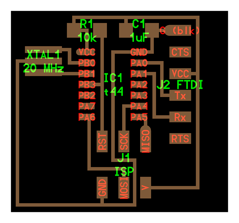
The first picture shows the board I had to recreate, I used the fab library to find the components and placed them on the screen you see in the middle.
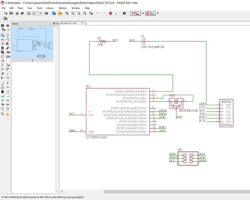
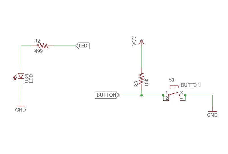
The second picture shows the schematic. This is a visual, easy to read representation of the components and their connections. This is also vital to create the final board.
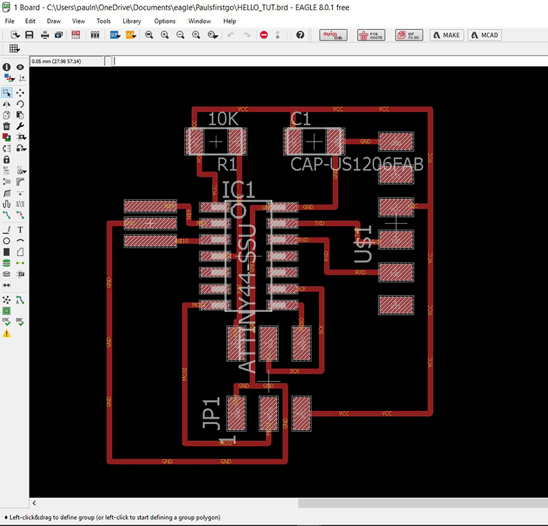
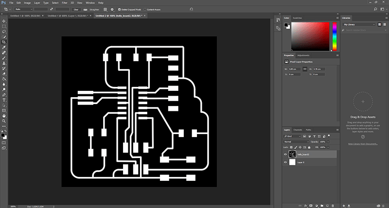
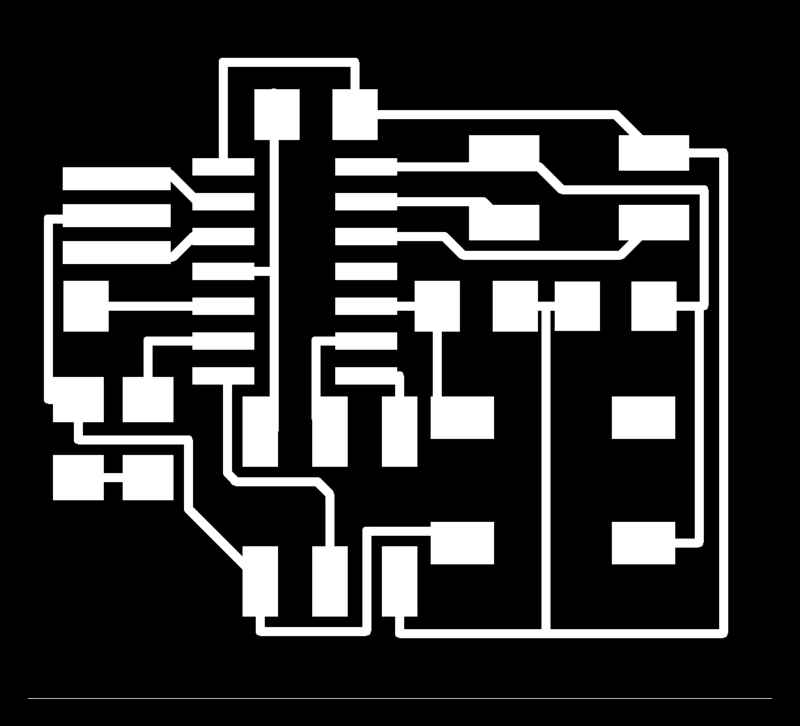
The third picture shows the board layout. This is where we create the actual paths to be milled by precisely placing the components and mapping the paths.
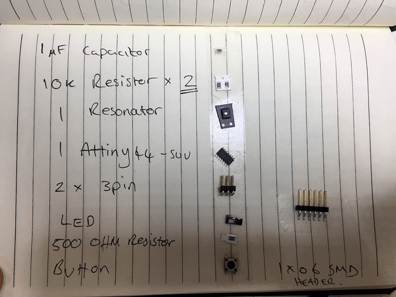
Next I have to add the LED and button to the hello_board along with a resistor
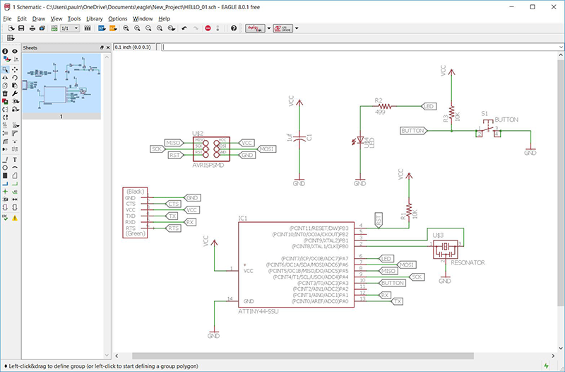
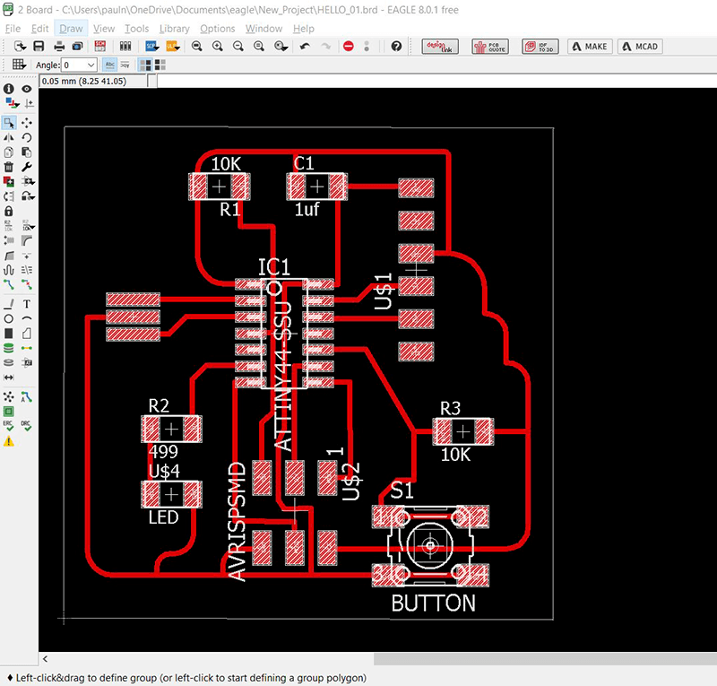
Again it was difficult to make it all fit within the tolerances. After reducing the grid spacing and discovering the different types of wires I could draw I ended up with a succesful board.
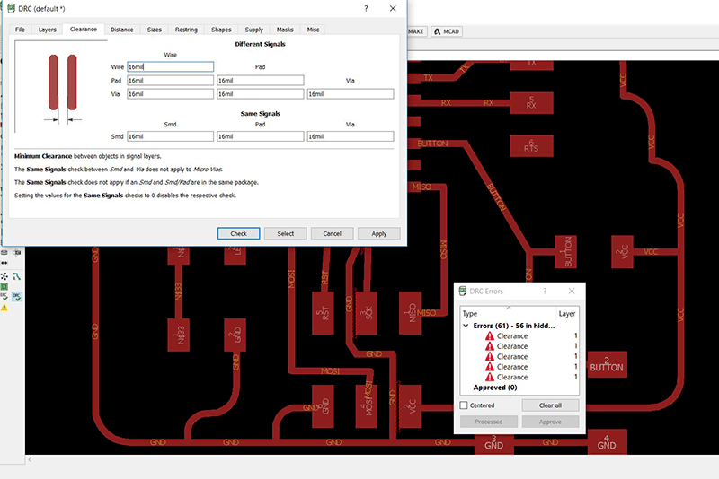
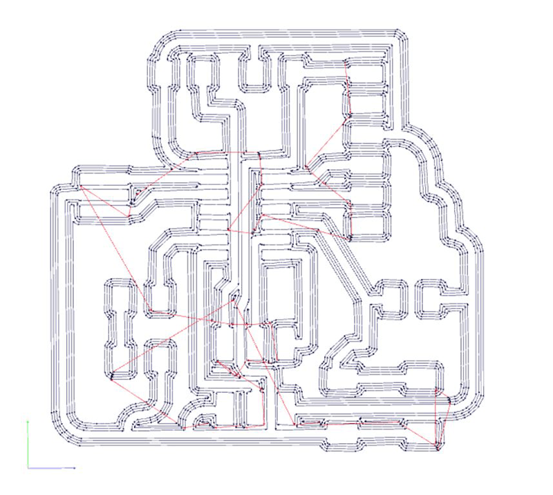
I had to confirm the board was within tolerance using DRC (Design Rules Check) to make sure I had enough clearance between traces. For this value I used 16mil (1mil = 1/1000 of an inch). This converts to 0.4064mm, so slightly larger than our 0.4mm bit. I found at times sometimes the traces were still not recognised as separate by FabModules (perhaps due to a resolution error).
It is worth mentioning there is an 'Autorouter', but I found this often led to the program creating a double sided board, which I did not want in this case.
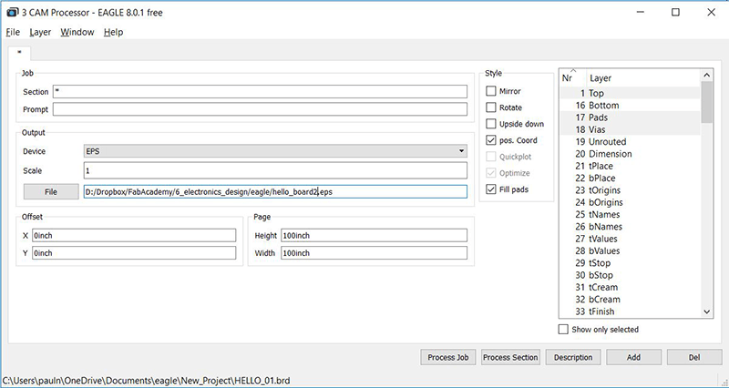
Finally the board was ready for export which I did by going File > CamProcessor and saving the top layer as an EPS file. I then used photoshop to edit (ctril + i to invert the image, ctrl + e to merge layers, SAVE AS as png) the board to create files ready for milling
I followed the same procedure as during the 'electronics production' week to mill using the Roland SRM-20. Unfortunately this time I was not so succesful and there were a few improvements I could have made on my work flow.
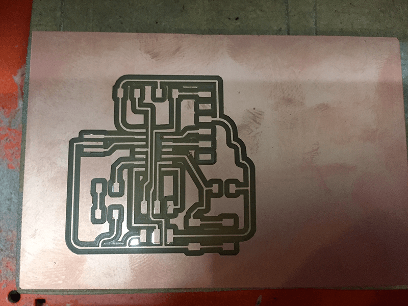
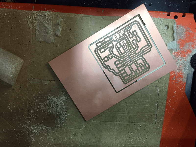
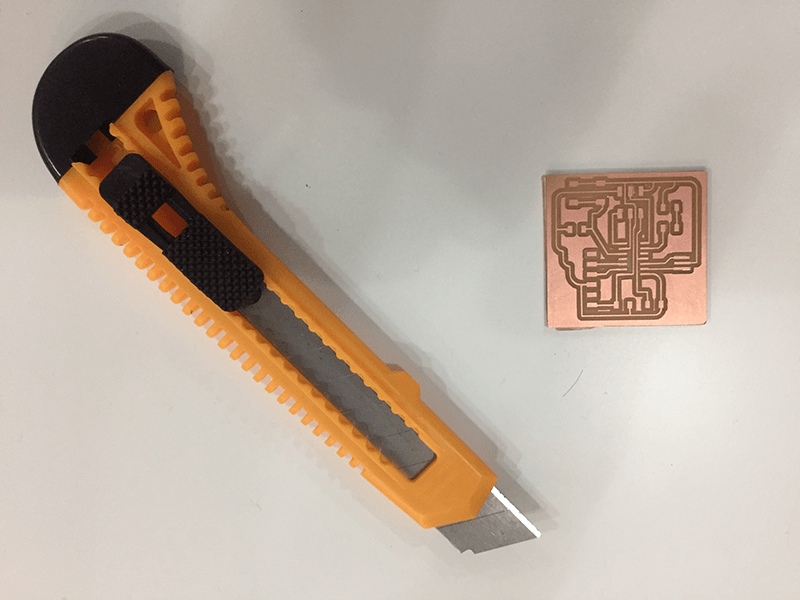
Firstly, I should have placed my X,Y zero much closer to the corner of the board, this would have allowed two PCBs to be cut from this one piece. Secondly, the board came loose during the milling of the outside using the 1/32" bit. Fortunately it had made 1 pass all the way around and was nearly all the way through when this happened, so it wasnt to difficult to free the board with a stanley knife. It did however lead to a rough edge that requires extra work that could have been avoided with a bit of extra care and attention at the beginning. Lesson learnt.
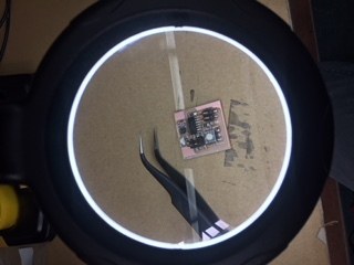
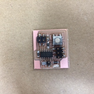
Now I have cut, it is onto the soldering of the pieces.
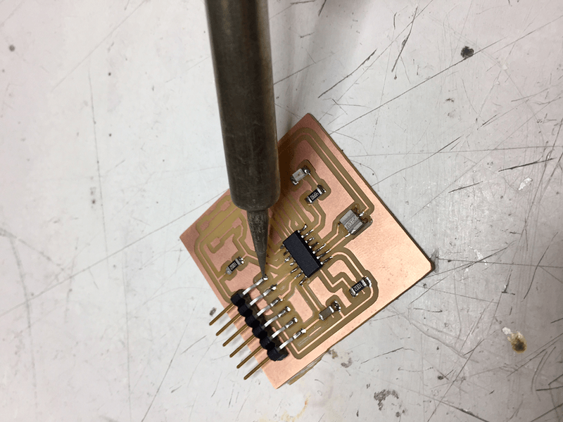
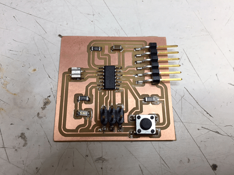
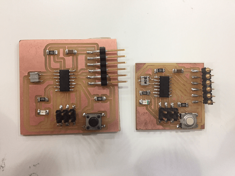
I was much more succesful at soldering after my first board. I did not have to reflow any of the solder at all and it looked pretty good by the end. The last image shows how much smaller I could have made the board and I will definitely look to do this in the future to save on materials.
I jumped ahead to get on with the board prgramming so click here to jump to week 8
2018 I made my board much smaller, removed some of the redundant FTDI pins and added an extra pin out to use if I need it.


I had an issue programming, after having a look under the microscope, I could see I had a dodgy SCK pin.
A quick reflow and it was working
Here you can find our group assignment page where we used an Oscilliscope to measure different aspects of our board.