Electronics Production
Assignment
group assignment:
characterize the specifications of your PCB production process
individual assignment:
make an in-circuit programmer by milling the PCB, then optionally trying other processes
Intro
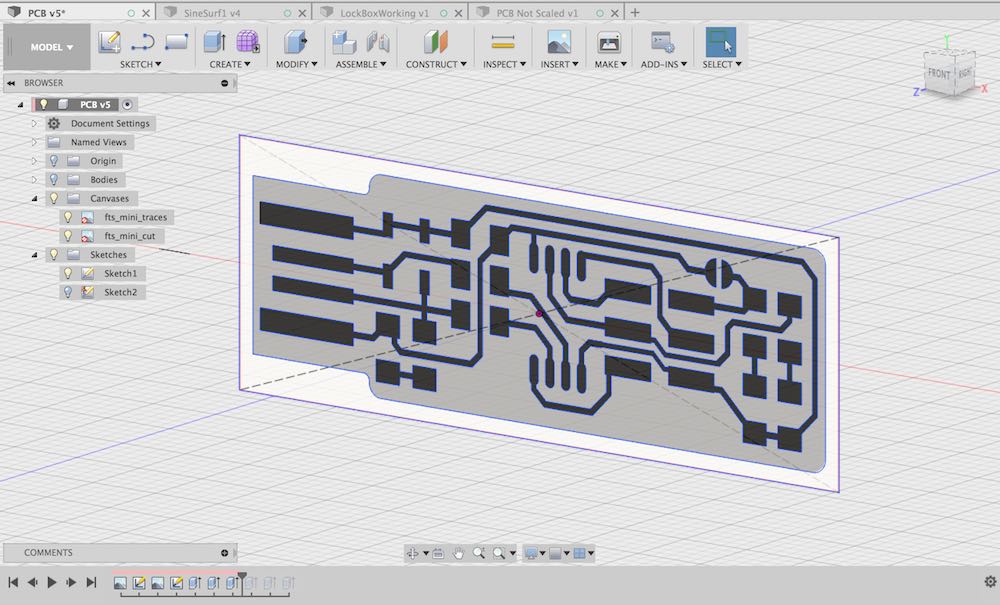
So I've built a lot of things, but I have no experience making circuit boards. I know EagleCAD is the autodesk's specific PCB design, CAD, and CAM software. I downloaded it and watched a couple tutorials but am still a little overwhelmed by the program and my lack of electronics knowledge, so I opted for just using other methods to get this board milled. A PNG file of the traces and board outline was all Brian's tutorial provided. I realized that I could probably trace the image in Inkscape and import the SVG to Fusion, but I wanted to trace it by hand in Fusion, to get a little more experience with the program.
UPDATE: Using FabModules was definitely the easiest, quickest way to get g.code for the PCB mill. That process is outlined further down the page.
Tracing
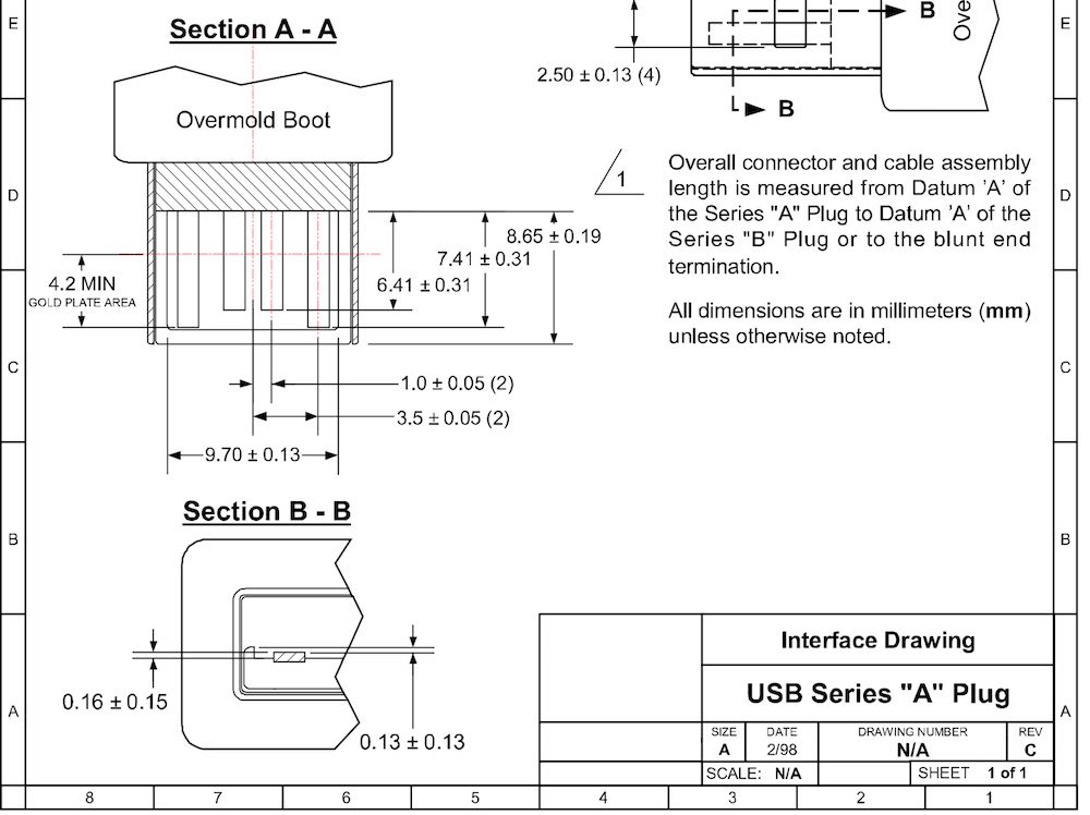
The calibrate feature for images in Fusion is very convenient and easy to use. I found references for the lead spacing on the ATiny45 that's specefied as well as for the spacing on the USB pads. I calibrated the canvas using the ATiny spacing and confirmed that scaling by measuring the USB pad spacing. Everything was within a couple thousands of a millimeter, well within tolerance.
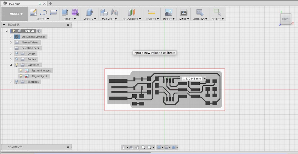
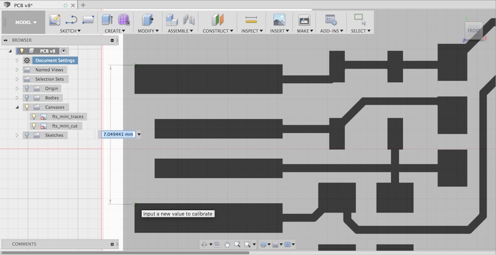
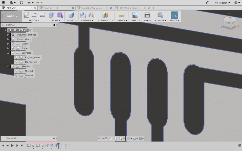
I really like the "smart snapping" in the Fusion sketch environment. It made the tracing a bearable experience. Once a few corners and lines have been layed out, most other geometry is in line with previously placed geometry and the snaps make the process intuitive and the drawing very regular.
Below is a short screen recording of the smart snapping that made sketching in Fusion so bearable. I would have recorded more of the process, but screen recording and running Fusion at the same time on my computer made things unbearably slow.
Modeling/CAM
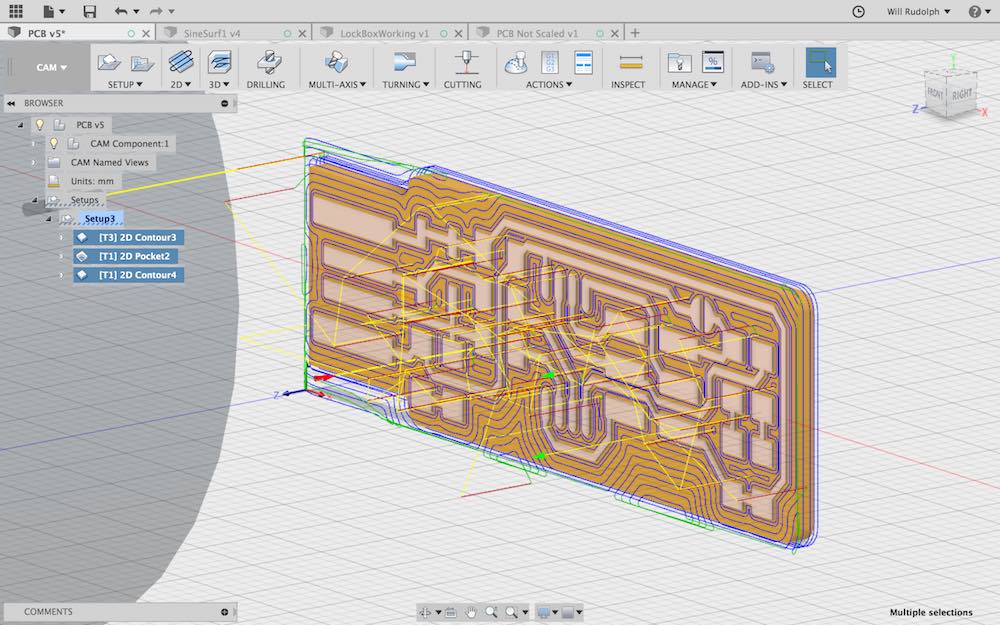
I was thinking about 3D printing some kind of case for this board, so I figured I'd model everthing to size from the beginnning. That way I can also simulate all the milling in Fusion and make sure nothing will go awry. I think you could also just make the toolpaths from the sketches, but I've been frustrated trying to do that in Fusion before.
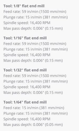
I found the correct speeds and feeds for milling FR-1 with the OtherMill listed on Bantam Tools website.
Using FabModules
This made the process a lot more simple and streamlined. Took a little time to get used to navigating. Had luck with fabmodules.org not with mods.cba.mit.edu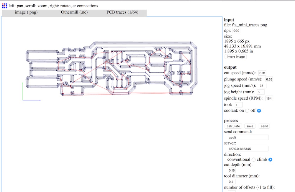
Milling
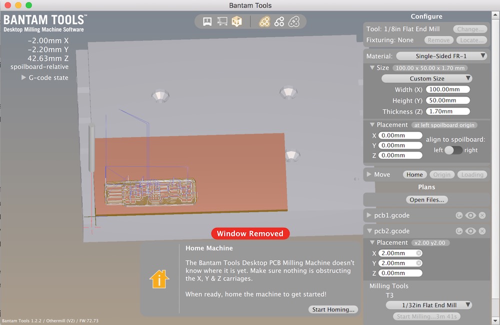
So our Lab's equipment for producing PCB's is the OtherMill Pro, a small desktop multipurpose CNC's with the required resolution for milling circuits. We have one sided FR-1 boards that seem to measure about 1.55 mm thick, 1.65-1.7 mm with double sided tape applied. We have 1/64th, 1/32nd, 1/16th, and 1/8th two-flute, flat-bottomed, carbide endmills available for these machines.
Othermill's proprietary software, Otherplan is quite intuitive and easy to use.
First, I began by entering the stock thickness, (including the thickness of any tape or attachment material) 1.7 mm. The xy size of the material is not essential to have exact for our purposes, I set it to 50 x 100 mm. This is such a small board, I'm going to use scraps of old pieces of FR-1 to mill. Otherplan very nicely shows a 3D rendering of the milling table with the stock shown at the size that is entered. Then when we load our .nc or .gcode files and choose a milling bit, the toolpaths and stock removed are simulated and shown on the material. This is very handy for confirming that everything looks as it should in our file. Homing the machine, changing out and locating new bits is as easy as following prompts from the OtherPlan software.
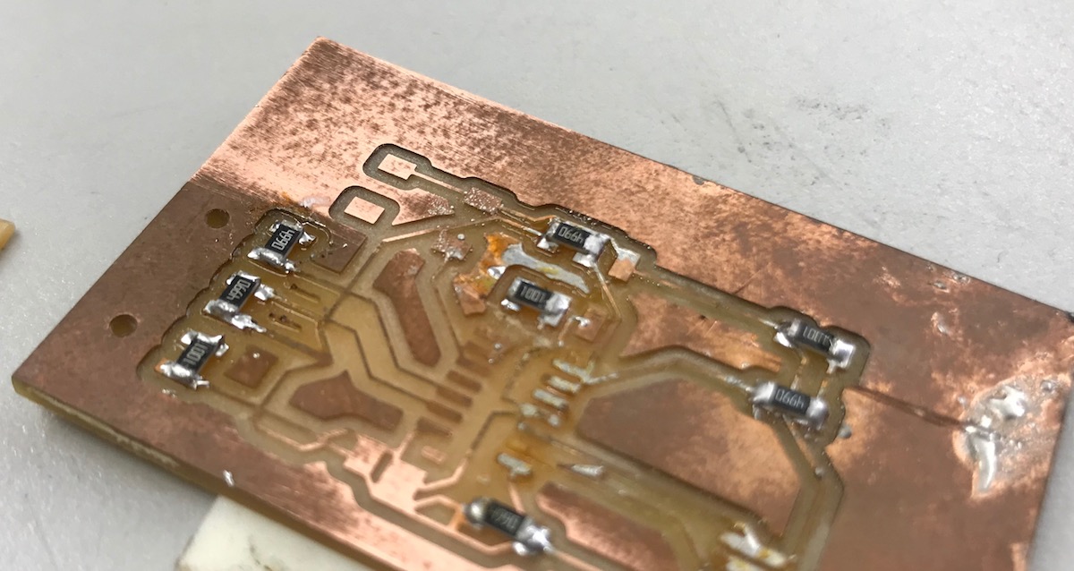
Though FabModules made generating the .gcode from the .png much easier, it limited my ability to alter toolpaths, and since I already had PCB modeled in Fusion, I figured I'd go with the toolpaths I created, rather than those generated by FabModules. Partly because we only had two 1/64th inch endmills left and I was the first to mill, so I didn't want to risk breaking anything. Taking that into account, I only ran a single tracing path with the 1/64th inch bit. For the rest of the stock I removed with a 1/32 bit. I just pocketed the remaining area to remove all of the copper. I havent seen any other boards that do this. I assume one ususally only mills around the traces simply to save time and cut down on tool wear. Finally, for the final outline cutout, I used a 1/16th inch endmill.
I was a little terrified starting the milling process I didn't want to break any endmills and we were already low on them. I though everything would go to plan, I had watched the simulation run in fusion, double checked all my measurments, double checked all my input values, and finally started the file for the traces. The first plunge was an anxious moment, but once the bit started milling everything looked like it was going well. After a few more moves and plunges I became comfortable with the macine running at the set speeds and feeds. The sound was quite nice (in the sense that I heard no undue vibration, chattering, straining, just smooth cutting. All the traces looked like the appropriate size, tiny. I switched out the 1/64th inch bit for the 1/32nd and continued on to run the next file that would clear out the remaining copper. Finally, I switched out for the 1/16th inch endmill to cut the board outline. I wanted to run through the process once more to get further aquainted with PCB work and to make a second board in case of catastrophic failure of the first. One thing I noticed while running the files on the first board is that if the board were cutout first, it would eliminate some of the material that was being cut by the 1/32nd bit. I figured less tool wear on the tiny bit would be better. Everything went smoothly again. I was so wrapped up in the excitement of the process and things going well that I did not take any photos or videos of the milling process.
Soldering
So I enjoy very detailed craft work and figured surface mount soldering would be a nice exercise in such work. I found this video (below) that gives a very nice overview of the principals and practices of soldering. It's a little dated, no surface mount parts, but does a very good job of explaining what good and bad solder joints look like and how to achieve them.
I got so concentrated and focused soldering that I forgot to take any videos or pictures along the way again. I kept in mind a lot of advice I've gotten over the years concerning detailed handwork:
-keep breathing calmly
-perform the actions taking the most concentration/stillness as you breathe out
-Keep a light grip on the your tools (soldering iron and tweezers), just enough to hold something and no more
-Move the workpiece constantly to find the best location and approach
-Check your work as you go
-Check your work when you're done
-Walk away, come back, and check your work once more with fresh eyes
I added the last piece of advice after I realized while looking at a picture of my board that I had completely missed solder on one pad. For very small detailed work such as this, looking at a photograph was incredibly helpful to check out things up close. The missing solder really jumps out in the last photo.
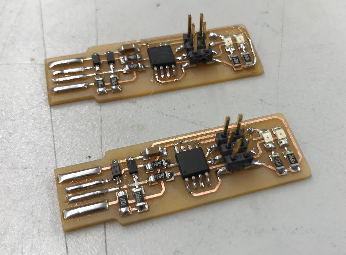
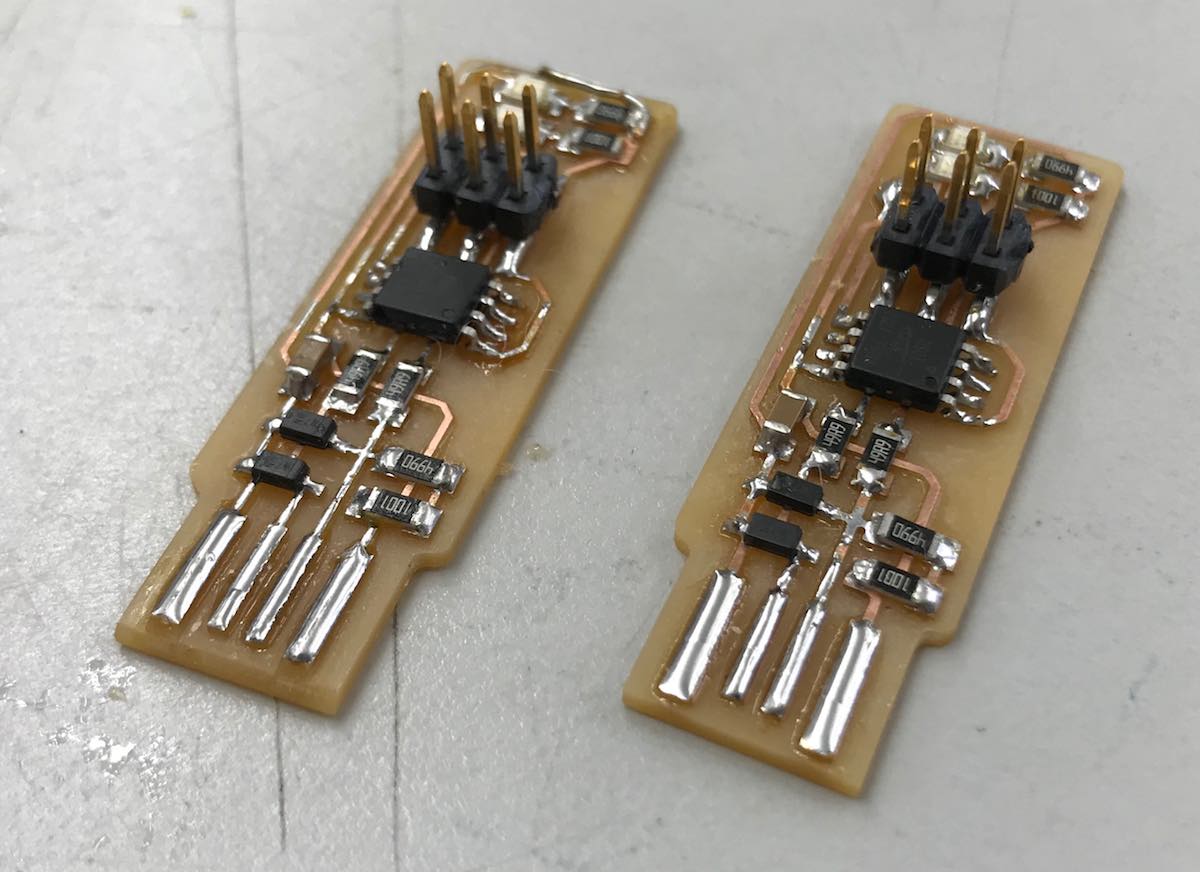
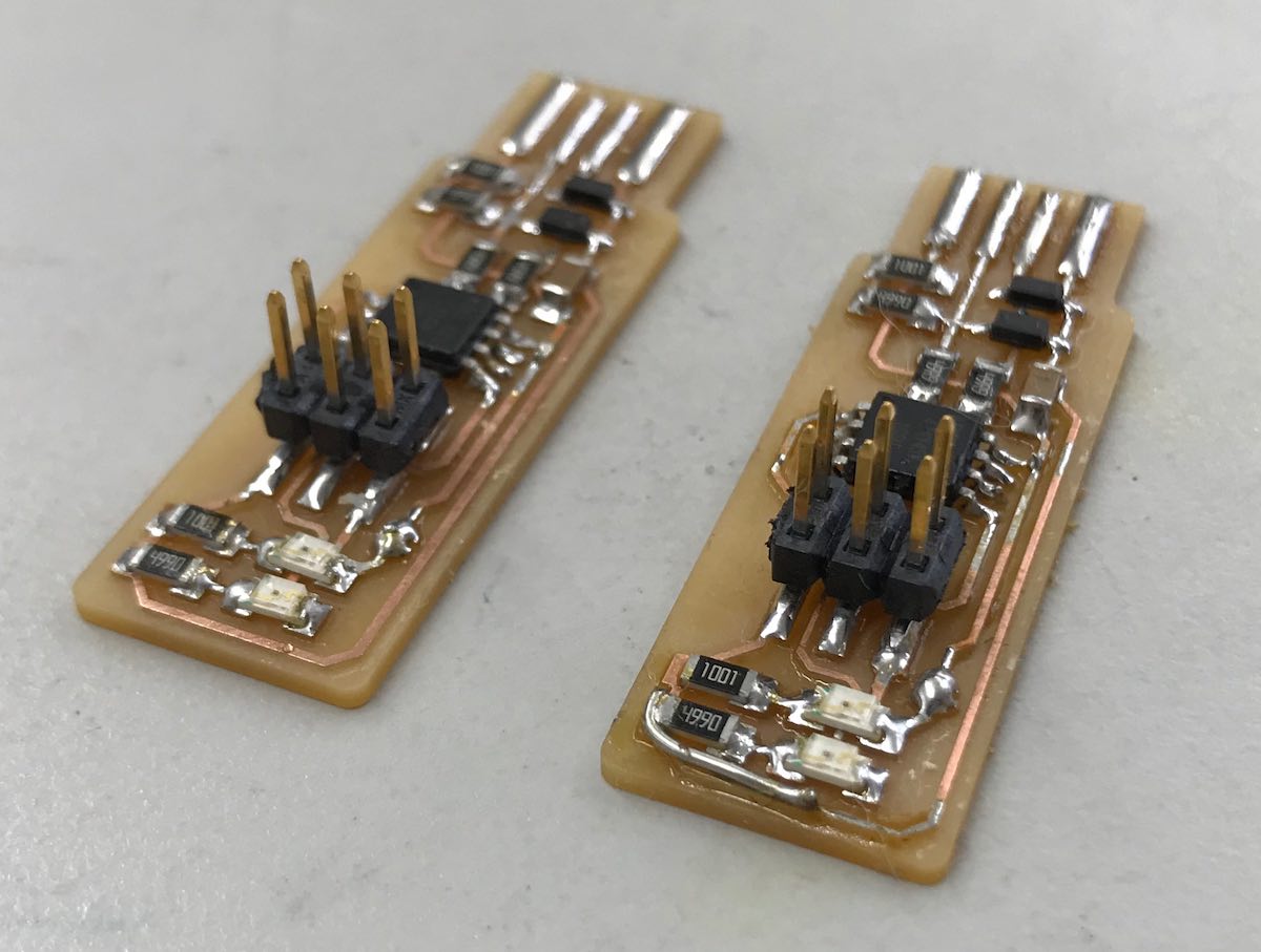
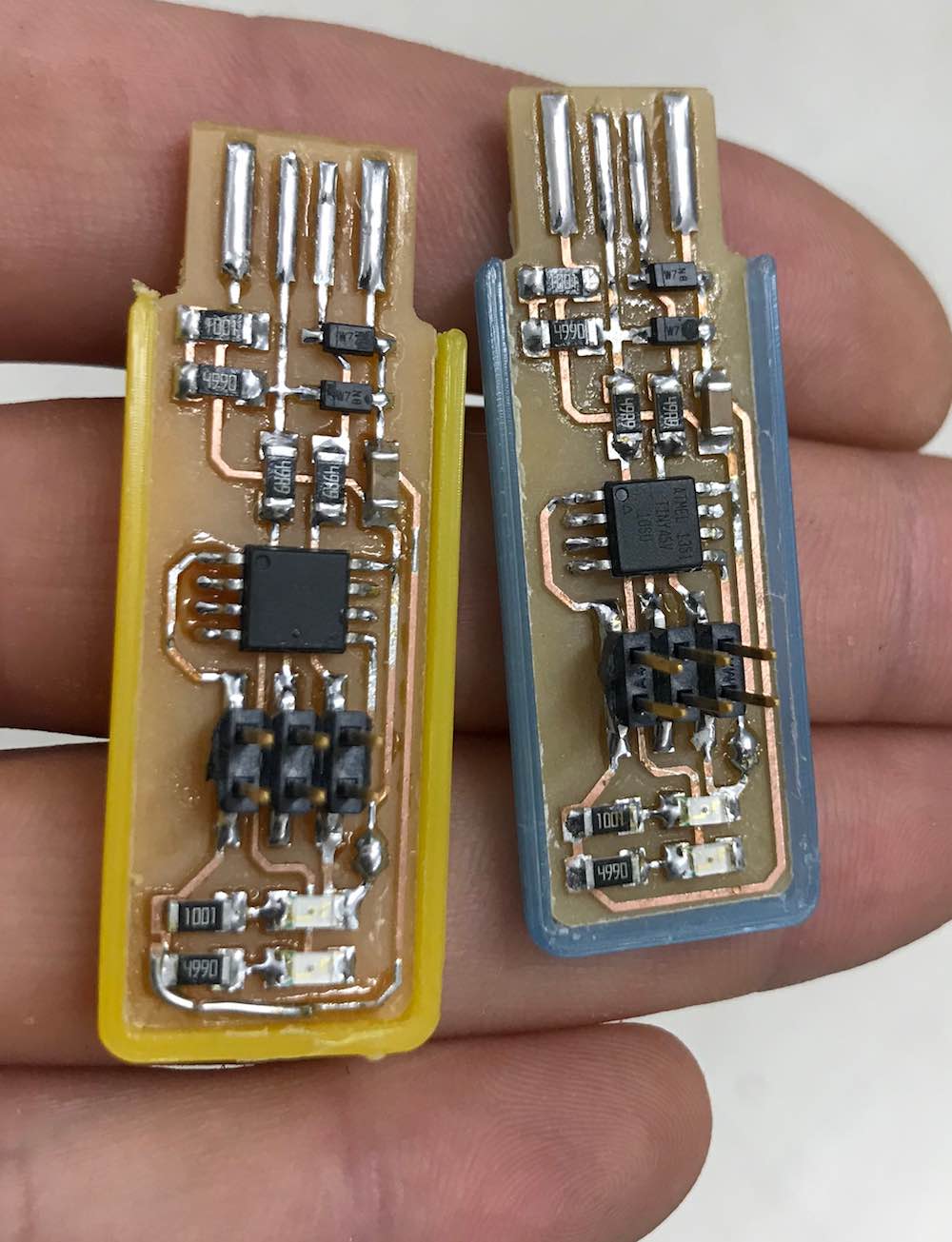
So I made two boards, assuming I'd make some mistakes while soldering, but surprisingly, the first one came out better than the second. Since I already had the fusion model, I quickly extruded a couple sketch elements to make a simple "case" and had a .stl ready to 3D print. With the cases attached, the boards fit snugly into a usb port. If you'd like to make your own, the .stl is included in this weeks files linked below.
To download my files click here: