Electronics Design
Have you:
[x] Shown your process using words/images/screenshots
[x] Explained problems and how you fixed them, including how you worked with design rules for milling (DRC in EagleCad and KiCad)
[x] Included original design files (Eagle, KiCad, Inkscape, .cad - whatever)
Group Assignment
For group assignments, there were two activities that really helped me with this lesson. First, at Fab Lab BCN both Fab Academy and MDEF students participated in a Club activity. Clubs are weekly projects that cover either: making, coding, or growing. The Club related to this assignment is The Resurrected Web. We covered: imaging a Raspberry Pi and connecting it to solar power in order to run a web server.
Group project:
Descriptions of diagnosing issues with the project can be found on individual student pages.
Adrien Laveau:
At Dassault Systemes, Greg Buckland held a session to cover continuity testing with a multimeter.
Continuity test Dassault Systemes:
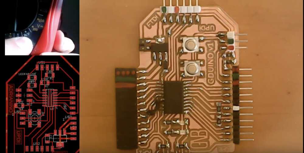
This is Greg showing the dial setting for continuity. It looks similar to a WiFi icon. If selected correctly, the leads of the VCC and GND will sound a beep alert when touching. In the multimeter that Greg demonstrated, the VCC goes in the center hole. The GND goes in the hole on the right.
The two straight lines indicate direct current. The dial is set to 20V to test if the microcontroller is receiving 5V. This is done after the board is connected to GND and a 5V power source such as an Arduino.
Back at Fab Lab BCN, we don’t currently have a working oscilloscope. I did however follow Carla’s documentation and reviewed an oscilloscope recitation:
Link to debugging recitation:
Link to presentation slides:
Individual Assignment
In the course of working on my final project, I visited Beach Lab in Sitges. There I worked on electronics design and programming with Francisco Sanchez Arroyo.
I had a couple of design constraints. At Beach Lab, there was one board of single sided FR-1. I worked in KiCAD to design the board. The concept of the board is something that would be usable throughout the project. I used an ATTiny44 for the microcontroller.
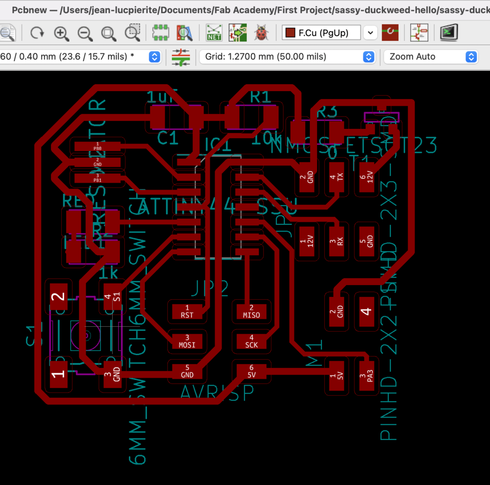
I then added a MOSFET P-CH 30V 1.1A SUPERSOT3. This is to connect to 12V and then power the board at 5V through the Drain of the component.
Datasheet:
I had a 0 Ohm resistor, which after some debugging I found that it was not soldered to the pad. I then switched out for a Zener diode. Originally the idea was just to skip over GND to connect the 5V line. Because the MOSFET cannot receive back 5V, the diode is there to block the flow of 5V into the MOSFET.
Datasheet:
I ran design rules checks on the board and made necessary adjustments. Then, I sent the PNG traces and outline files to the OtherMill through the Mods community project.
Finally, I programmed the board with the Micro USB Tiny AVR ISP. I switched the pins around on my boards ISP header. So, I after I successfully flashed the board; I wrapped the connectors with tape. That way, I can plug and unplug from my custom header.
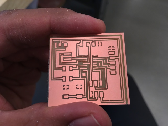
Hero Shot
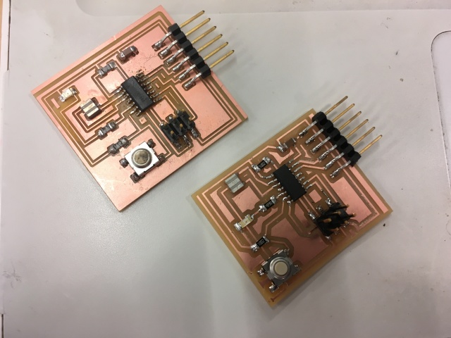 Two versions with and without ground plane.
Fabricating the Board
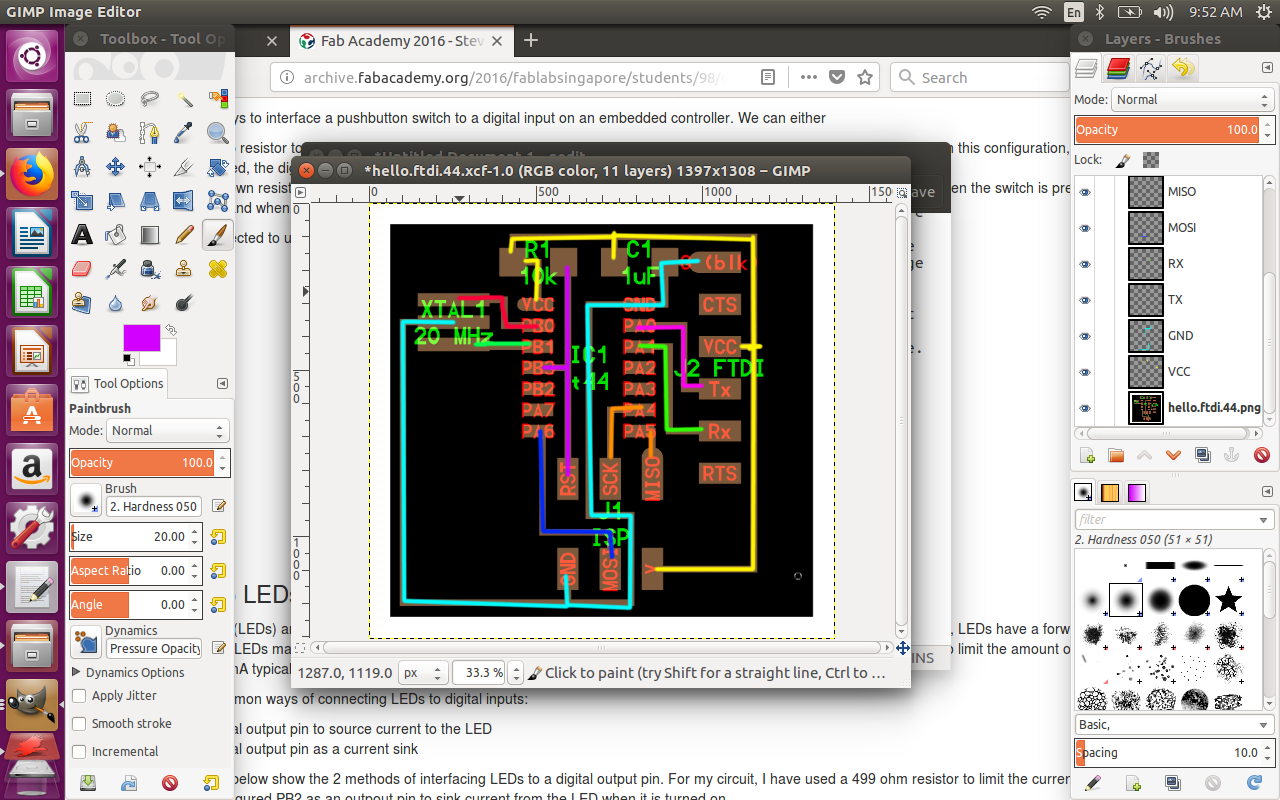
The first step was to download the board preview for hello FTDI 44. In GIMP, I created a new transparent layer named VCC. I traced the connections on the board preview with a distinct color. I repeated that process for all layers. These are the descriptions of the connections from the ATTiny44 datasheet:
VCC - Supply voltage GND - Ground TX PA0 - ADC0: ADC input channel 0. AREF: External analog reference. PCINT0: Pin change interrupt 0 source 0. RX PA1 - ADC1: ADC input channel 1. AIN0: Analog comparator positive input. PCINT1: Pin change interrupt 0 source 1. MOSI PA 6 - ADC6: ADC input channel 6. DI: USI data input three wire mode. SDA: USI data input two wire mode. OC1A: Timer/Counter1 compare match A output. PCINT6: Pin change interrupt 0 source 6. MISO PA5 - ADC5: ADC input channel 5. DO: USI data output three wire mode. OC1B: Timer/Counter1 compare match B output. PCINT5: Pin change interrupt 0 source 5. RST PB3 - Reset input. A low level on this pin for longer than the minimum pulse length will generate a reset, even if the clock is not running. SCK PA4 - ADC4: ADC input channel 4. USCK: USI Clock three wire mode. SCL: USI Clock two wire mode. T1: Timer/Counter1 counter source. PCINT4: Pin change interrupt 0 source 4. XTAL1 PB0 - XTAL1: Crystal oscillator input. PCINT8: Pin change interrupt 1 source 8. XTAL2 PB1 - XTAL2: Crystal oscillator output. PCINT9: Pin change interrupt 1 source 9.
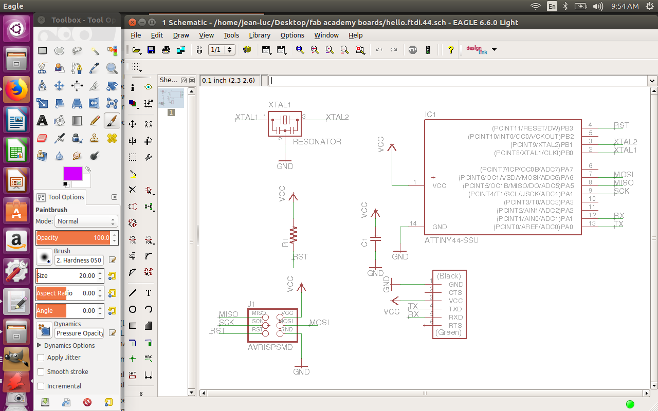
Reviewing these connections for documentation pointed out that I missed connecting PB3 to the other RESET connections. I opened the file in Eagle and corrected the schematic.
I cloned the FabAcademy Resources repo from GitHub. When I opened Eagle, I added the path to the downloaded lbr and dru files. It's important not to replace the default paths in Eagle, as symbols are needed from the included libraries.
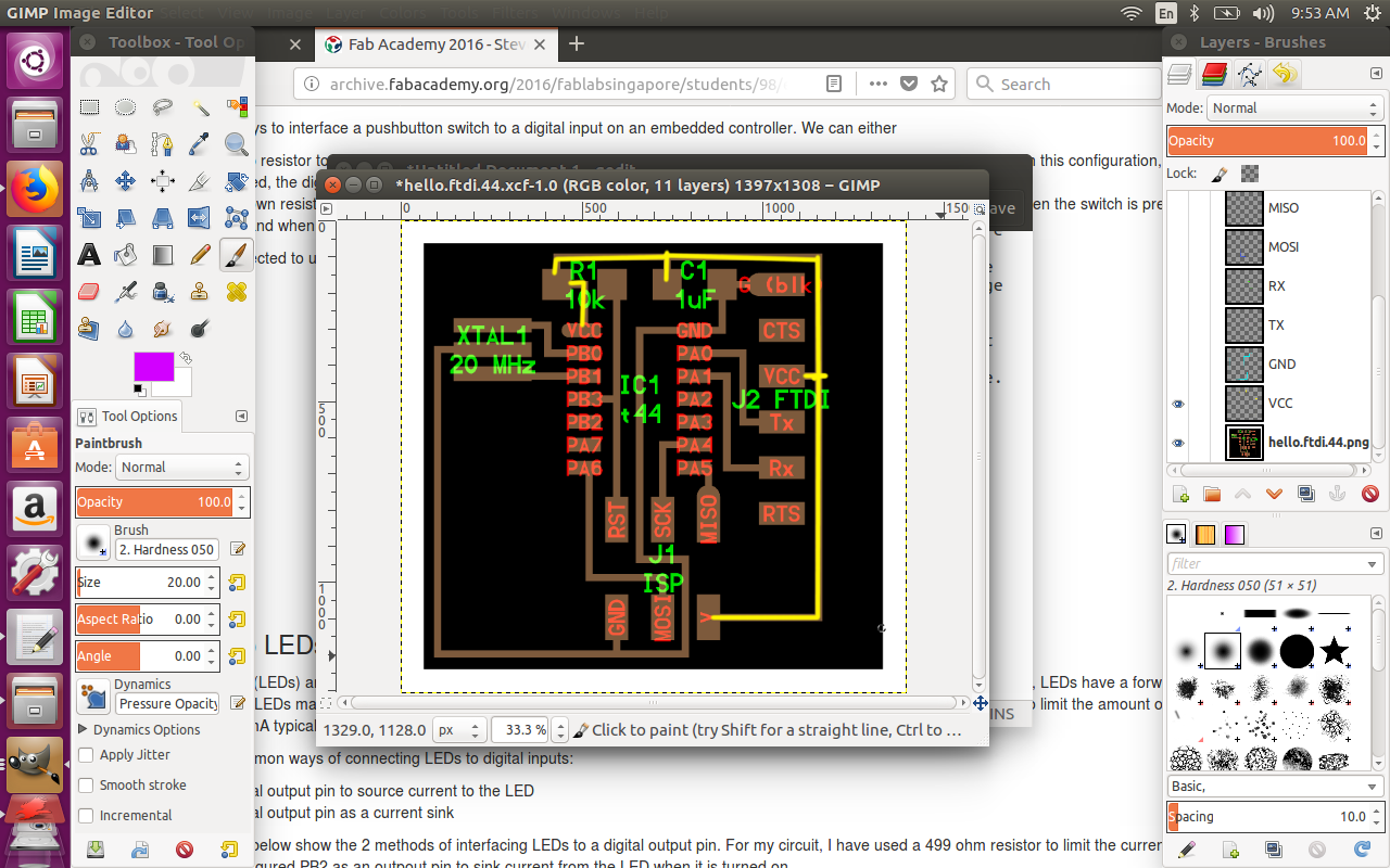
I began placing the components from the fab library. VCC and GND symbols are in a supply library. Using nets and labels, I then started to make connections following the highlights in the GIMP file. I switched layers on and off as I progressed to place components and make connections.
Steven Chew connected the Pushbutton Switch with a 10k pull up resistor tied to PA7 "to tie the digital input to a logic 1 and connect the pushbutton between the digital input pin and ground. In this configuration, everytime the pushbutton switch is pressed, the digital input will be pulled low. When the pushbutton is released, the digital input reads a logic 1."
For the LED, Steven "used a 499 ohm resistor to limit the current through the LED to about 6 mA. I've configured PB2 as an outpout pin to sink current from the LED when it is turned on."
I found a couple of YouTube videos to walk me through the copper pour technique that Steven used. Once the Design Rule Checks were passed and there were no more airwaves, I exported the file for milling through FabModules.
Milled out version with ground plane pictured above. After stuffing this version, I received:
avrdude: initialization failed, rc=-1
         Double check connections and try again, or use -F to override this
check.
This first iteration of the board, the LED lit up. That was due to a solder bridge...
I sought advice from Luciano Betoldi. We tested the board with a multimeter, which was inconclusive. Luciano advised that the ground plane adds an air of mystery to whether there is electrical interference in the circuit. I ultiamtely decided to redraw the board in Eagle. The second iteration. I was successful in sending code to the board.
Design files: Right click + Save As
- Design files: Right click + Save As
Background
Since I began with The Fab Foundation, I helped support two cycles of Fab Academy. While my main preoccupation with Fab Labs is procuring and deploying inventories for new installations, I also help procure supplies for labs running Academany courses. While most requests come in the form of shipping out end mills or FR-1, the most involved request was the procurement and distribution of Stage Kits for the Machine Making assignment. It was during my second go in 2016 of shipping out stage kits that I got my first big lesson in Electronics Design.
We switched vendors to Seeed Studio to supply gestalt nodes. Not knowing any better, I did a simple git clone of the gestalt single stepper node repository and sent it along with our quote request. This was my first time dealing with a board house. Thankfully, Seeed and other such board houses provide helpful walkthroughs of the actual ordering process. Instead of referring me to such a page, the representatives at Seeed were very generous and attempted to gather the necessary information over email. They needed: Gerber files, a Pick & Place file, PCB technology specification, and a Bill of Materials. In addition to those files, they requested several changes to the gestalt node (at that time it was rev 0.3).
Seeed provides files on their “Fusion” ordering page which are used in Eagle CAD. There are design rules files for two and four layer boards. There are also CAM processor files to export Gerber files for two and four layer boards. The gestalt node is a four layer board with through holes. So, I downloaded the DRU and CAM files for four layers. I copied each file into the Eagle sub folders for design rules and cam processors. I made a new folder under the projects sub folder. I then copied the board file and schematic for gestalt node rev 0.3 into the new folder. Setting up the files for Eagle was all done outside in Finder on Mac OS X.
Design Rules Check (DRC) is accessible in Board View under Tools -> DRC. This will default to the Eagle Default DRC. Once the window is open, the “Load…” button gave access to the Seeed DRC. Once the check is run, the design rules are copied to the board. Running the Seeed DRC on gestalt node rev 0.3 generates quite a few errors mostly with Clearance, Keep Out, and Stop Masks.
Menus in Eagle are context sensitive (at least in Mac OS X). To export Gerber files for Seeed, (once again, in Board View) I went to File -> CAM Processor. With the CAM Processor window open, I went back to File and selected Open -> Job. This opened the cam processor sub folder and I was able to load the Seeed Gerber processor. Eagle does include Gerber processors. Depending on the board house, you should download and process your PCB design according to their requirements. One of the best explanations that I found of Gerber files was on Maxembedded.com. In an article describing PCB Design, Soumil Heble says that Gerber files are PDFs of your PCB for manufacturers. These are final copies of the layers that are not meant to be edited. So, what happens when your Gerber files cause problems for the manufacturer?
In my haste to meet a deadline (fabrication and shipment of boards from China to Boston take up to five weeks), I neglected the list of Design Rules errors. Seeed did have the Board and Schematic files for the gestalt node rev 0.3. So, they were able to supply a Design For Manufacturing (DFM) Feedback Report. This report of issues was categorized by level of seriousness between cool and hot. Hot meant the issue was a “manufacturing or reliability show stopper”. Cool meant the issue had a “low impact on cost, quality or cycle time”. Nothing on the list was Hot; yet, minor moves and adjustments needed to be made to address issues that were “Warm” or “Cool”. The issues were: “0805 package distance is too small, recommend to adjust to 0.75mm; silk screen are still on pad, need to move; There is no direction mark of IC6; Via holes are on the pad, need to move.”
We facilitated a little back and forth negotiating between Seeed and Nadya Peek. Adjusting the location of the 0805 package components would have required Nadya to change the board significantly. Seeed confirmed that we were able to go ahead with the present pad positions. The reason for such clearance concerns is that components of differing signals could influence each other if spaced too close. By Seeed’s rules, the components should be spaced 0.75 mm apart. Still, we were able to go forward with the job by only moving the silk screen and via holes away from the pads. We also added a direction mark to IC6. With those minor adjustments, we had gestalt node rev 0.4.
The experience with the Gestalt nodes was enough of a base to familiarize myself with Eagle CAD. I was able to: add components, nets, labels, values; and route or rip up traces. What I needed to connect the dots was a better understanding of trace widths. There is a good explanation on Stack Exchange which includes a nomograph for trace calculation. (http://electronics.stackexchange.com/questions/5403/standard-pcb-trace-widths\ or signal traces. The board milled out correctly after those adjustments.