Electronics Design
I got started this week by installing SolidWorks PCB on my laptop. First, I modified my existing install of SolidWorks 2018 to get the add-in and standalong PCB software, and then I installed the server component of the PCB software (also on my PC).
I watched a quick YouTube tutorial to get my bearings and then began the process of building out my library of standard components. At first, it was very slow-going as I found myself scouring through the Altium website trying to figure out which supplier catalog I needed to download for each component. I was quickly becoming jealous that the FabAcademy had a pre-built library for Eagle. Thankfully I found out that I could import the Eagle library into SolidWorks PCB! This saved me a huge amount of time!
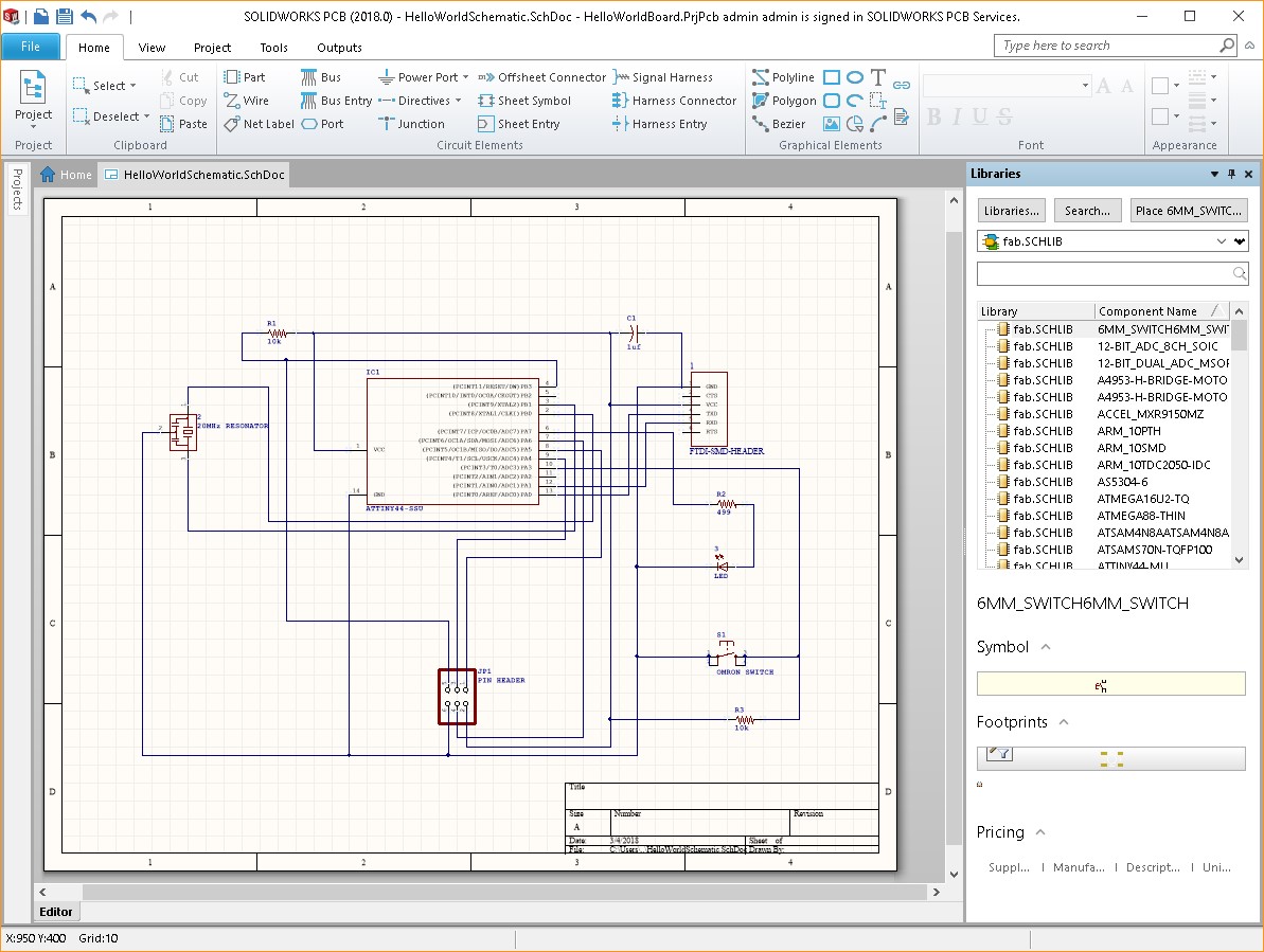
Library in hand, I could then turn my attention to laying out my schematic. I placed the components on my sheet and then began running wires to connect the various pins. I like how at this stage of the process, you can ignore the complexity of trace layout and just focus on making sure teh right pin is connected to the right component.
Here's what my schematic looks like:
With the schematic laid out, I turned my attention to the PCB. In SolidWorks PCB, you can either start in the PCB software and push the shape of the board to SolidWorks, or start in SolidWorks and push the board shape to SolidWorks PCB. I had a very specific board shape in mind, so I started in SolidWorks.
I grabbed an image of the Millenium Falcon from Google and inserted it as a sketch picture so I could trace it to define my board outline. I made sure to scale the image so it resulted in a board that was smaller than 2.5" x 3.0"
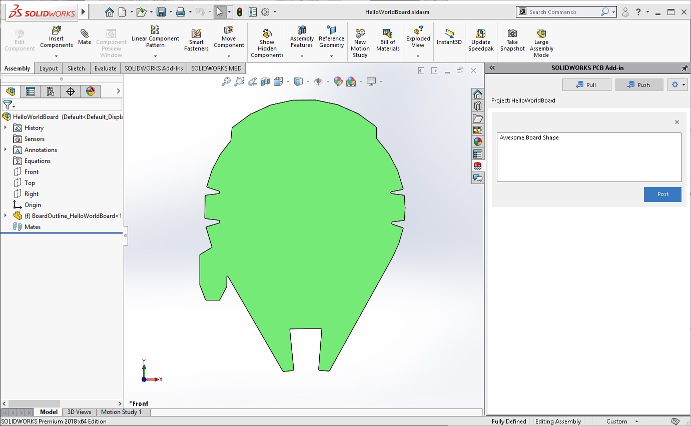
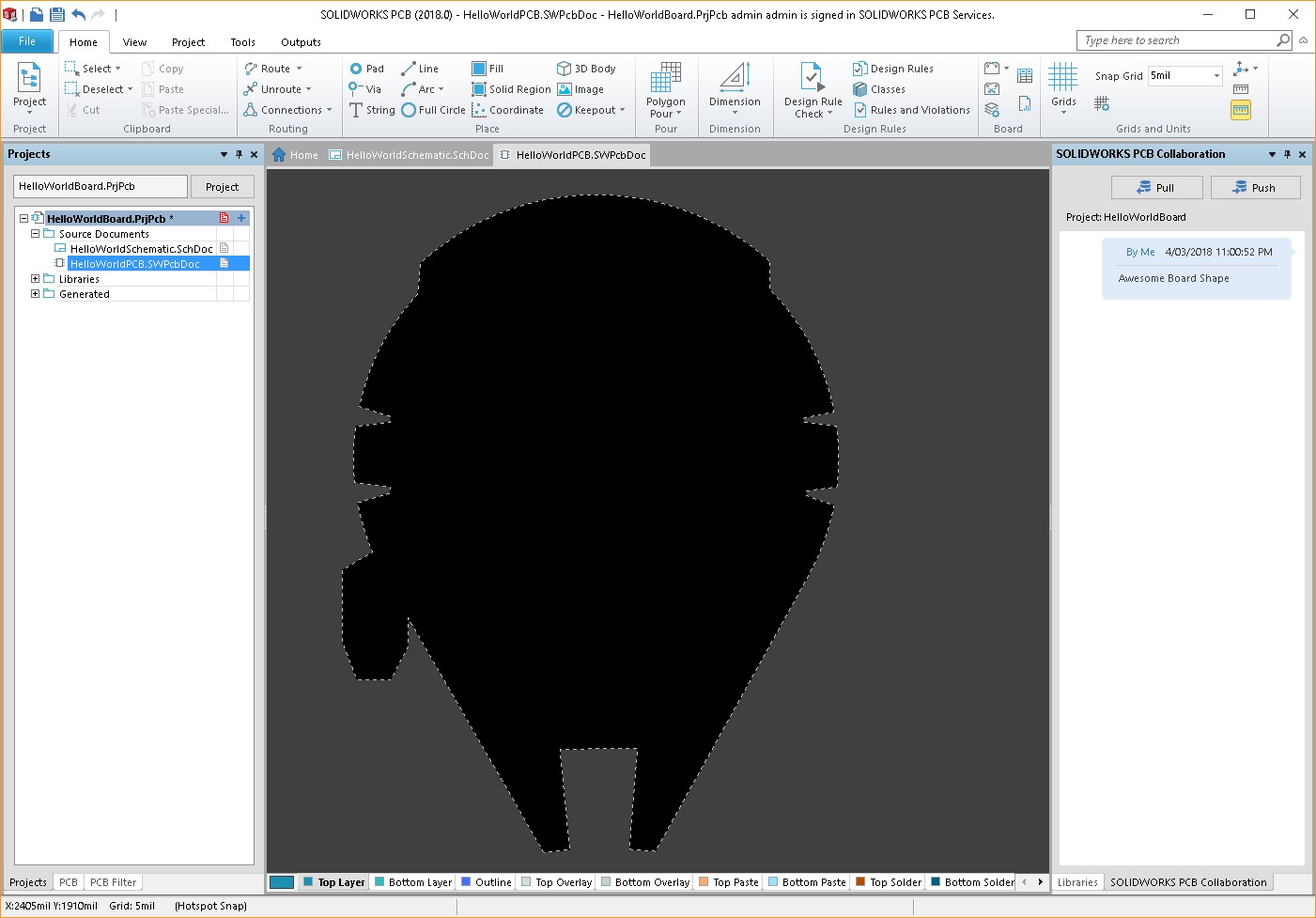
Then I "Pushed" the board shape from SolidWorks, and "Pulled" it from SolidWorks PCB.
At this point, I could read the schematic information onto the PCB to populate the board with components. The full list of items comes in off to the side, so all I had to do was drag them into a desired location. This was my inital layout:
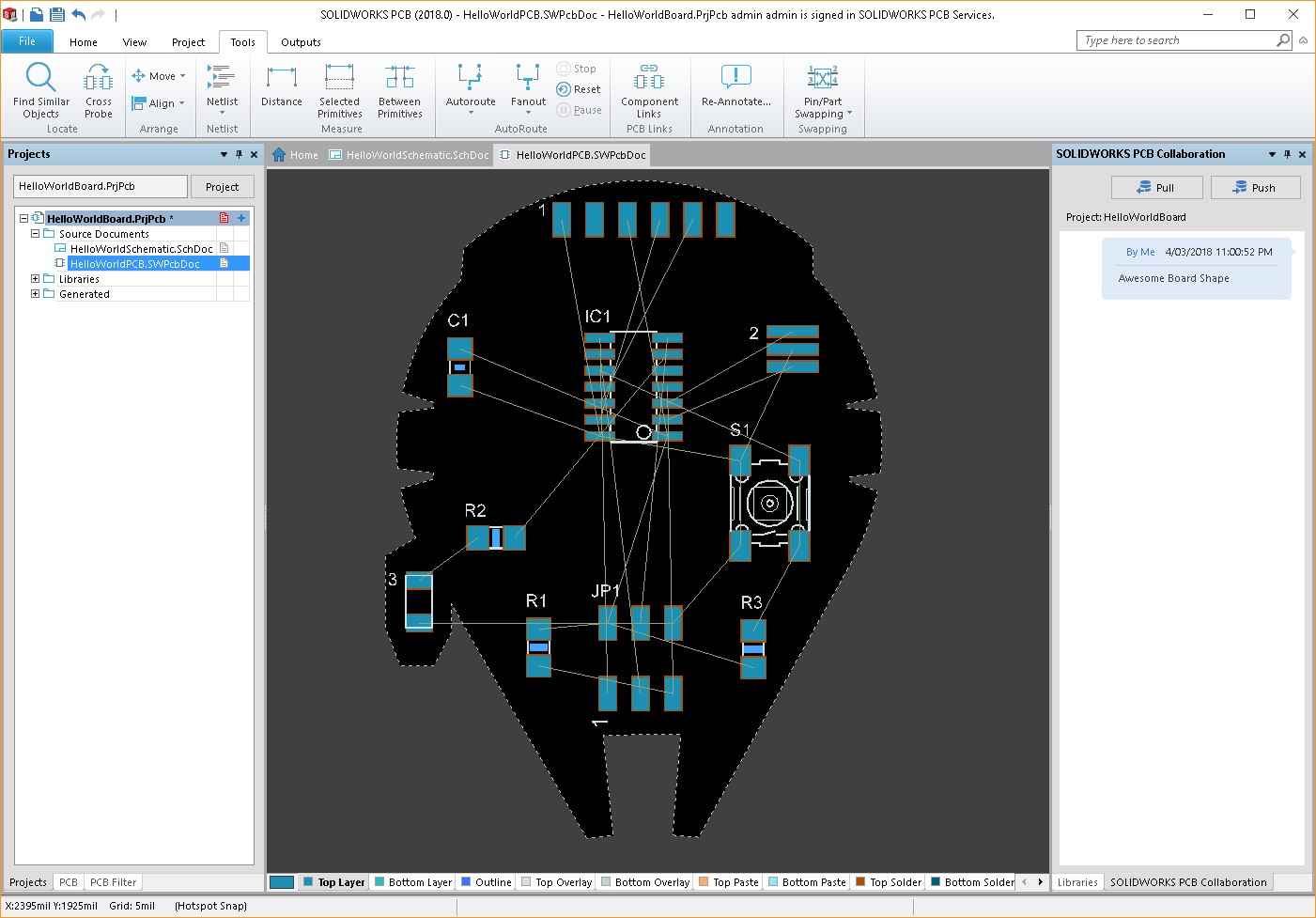
I chose it because I was trying to mimic the aesthetic of the Millenium Falcon. I specifically wanted to achieve the LED placement in the cockpit.
I tried to use the software's autoroute functionality to place the copper traces, but I didn't have enough luck. It works fairly well, and to be fair, I didn't realize early enough that I should have tweaked settings like trace width and minimum clearance values to help it find better solutions, but ultimately, I ran the traces manually.
This process turned out to be really straightforward, and allowed me to better visualize and understand how things were connected on the board. Also, because I was able to focus on a small part of the challenge at a time, I was able to achieve an even better placement of my components.
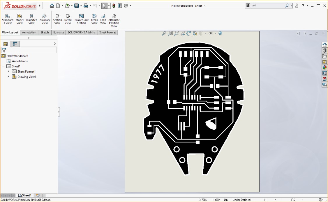
Here's what the final board layout looks like:
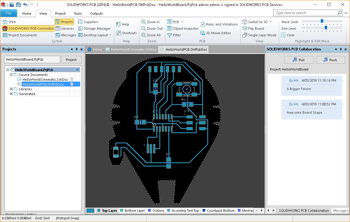
I'm really quite pleased, as I was not only able to get the LED in the location I wanted, but I also created a layout that - to me - looks a bit like Darth Vader's face when you see it for the first time without his helmet!
A "normal" person might be content to cut the PCB at this point, but not me! I wanted to customize it a bit more. I tried to push the copper back to SolidWorks, but found out that this doesn't work with the imported library from Eagle - I guess it lacks some information (found in the Altium libraries) that SolidWorks needs to build the 3D geometry. Refusing to let that get in my way, I exported a Parasolid file from SolidWorks PCB and then opened it in SolidWorks.
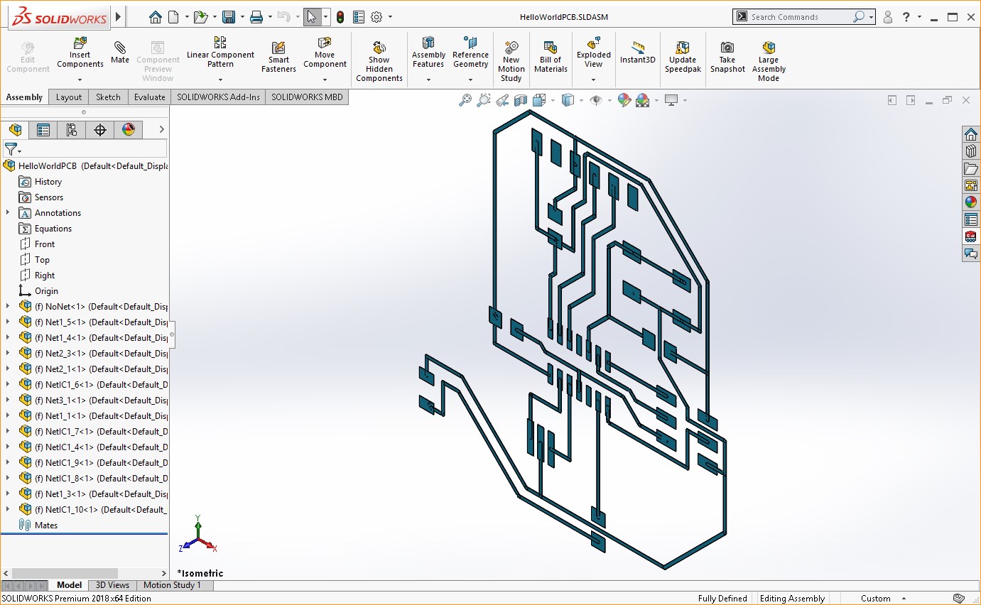
The copper came in as an assembly of parts, but I only wanted it to be a single part, so I inserted a new part in that assembly, edited it in context, then created a "Join" feature to add all of the geometry in the assembly together to form a single part. I then used that part in conjunction with the board I originally modeled to produce this shape:
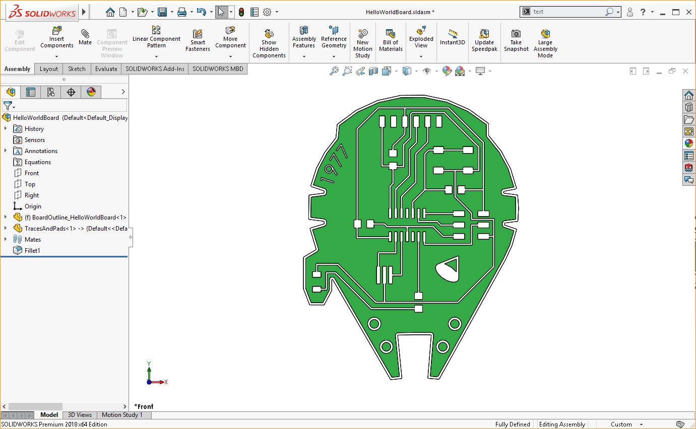
As you can see, I added a few more details, including "1997" - the year "Star Wars: Episode IV - A New Hope" came out in theaters.
I created a drawing of this model as well as one of the board outline, and then saved each as a seperate PNG file that I could use to cut the board on the Roland SRM 20 MonoFab.
I then used MODS to cut the traces on the board.
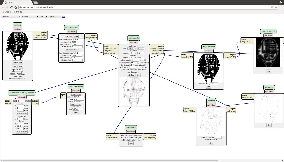
I used a 1/64" bit to cut the traces and a 1/32" bit to cut the interior holes as well as the perimeter.
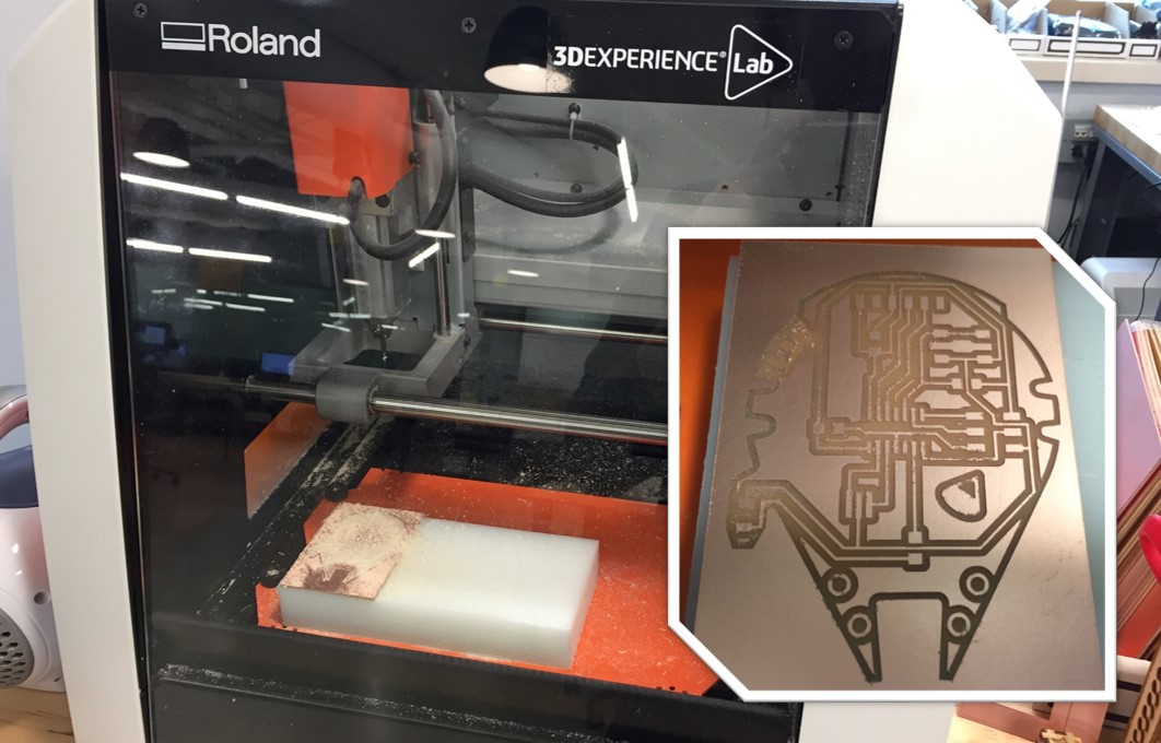
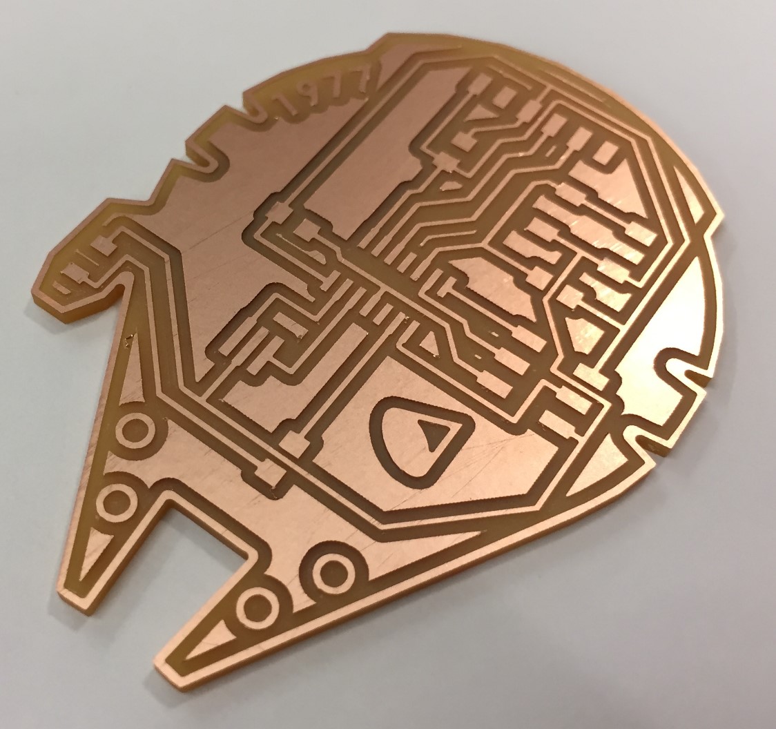
This is what the board looked like right off of teh milling bed.
I learned a good lesson when I attempted to cut the perimeter. It turns out that MODS doesn't like a thin line as a perimeter. There needs to be more pixels (I believe the threshold is 20) for the path to properly calculate. When I ran the thin perimeter through MODS, it produced a random squiggle of a tool path.
Thankfully, correcting this was easy enough... I simply edited the PNG file and filled the area outside the design in black.

This nicely cut the part so I could remove it from the bed.
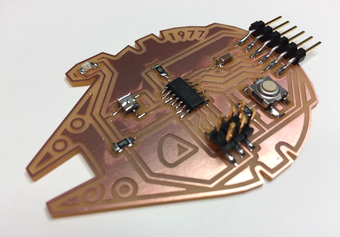
I drew a visual parts list and taped the electronics components to it so I could easily keep track of the tiny parts.
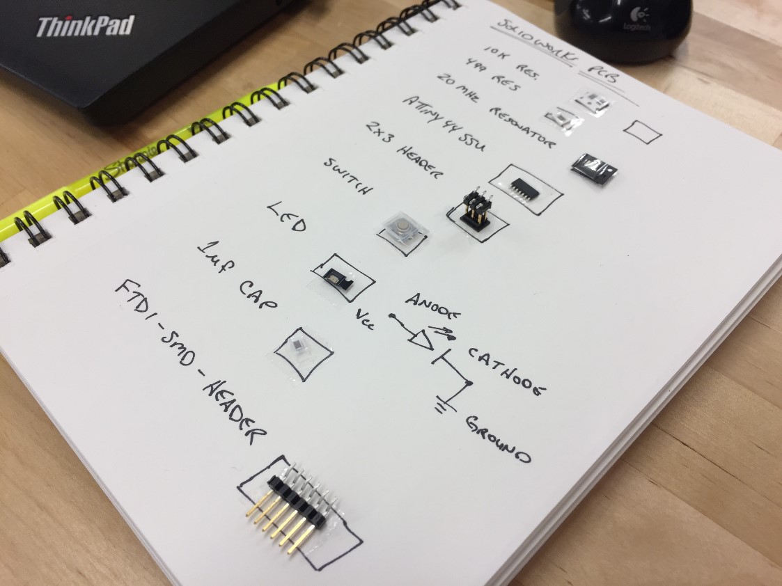
Then I soldered the components to the board, taking my time to produce smooth joints. I must say, the resonator gave me a bit of trouble. I think I'll make the soldering pads a bit longer in the future. That way I have a bit more room for the soldering iron to make contact.
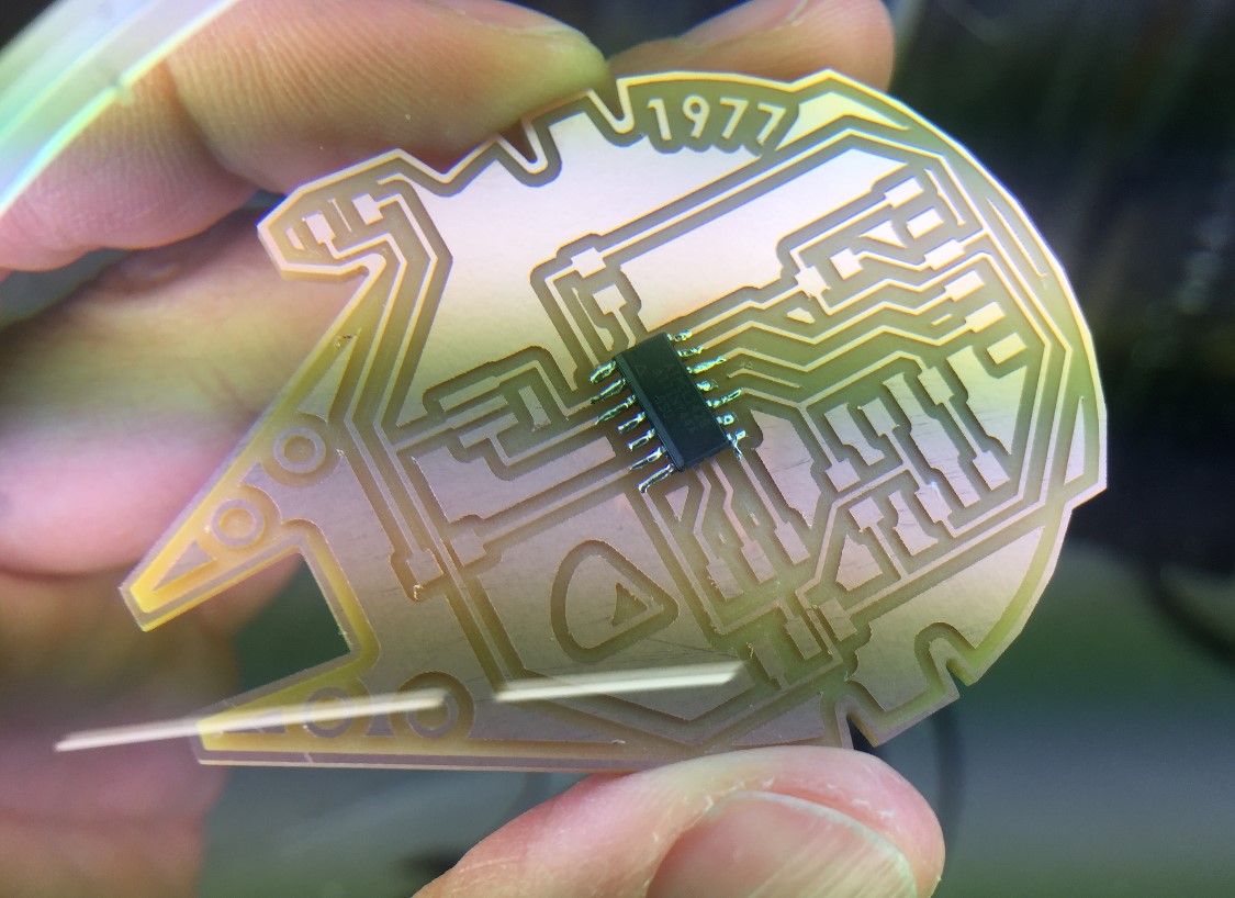
Here's the finished board! ...Cool, huh?