Back to Mejdi_FabAcademy_FollowUp

Week7: Electronic design

Assignment:
- redraw the echo hello-world board,
- add (at least) a button and LED (with current-limiting resistor)
- check the design rules, make it, and test it
- extra credit: simulate its operation
- extra credit: render it

Designing the "Nano Fab ISP" with KiCAD

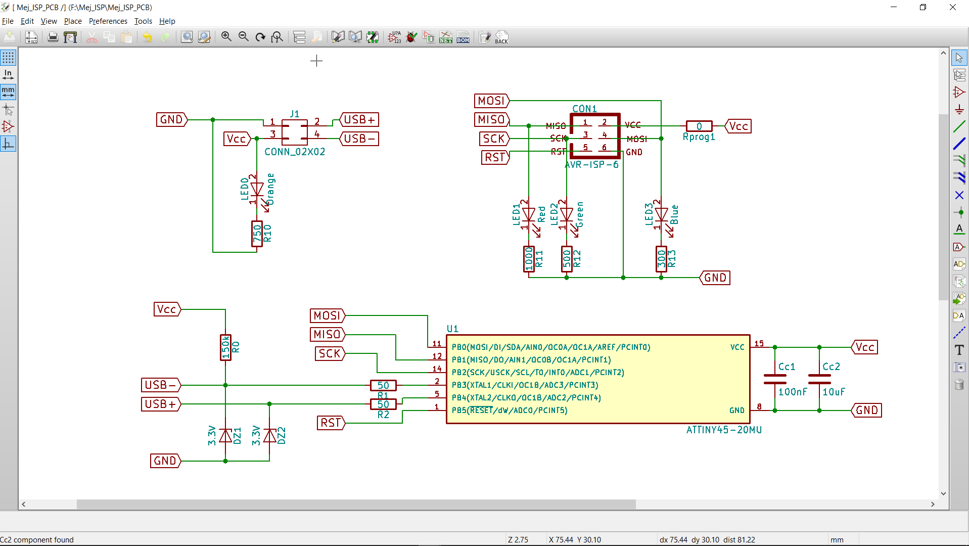
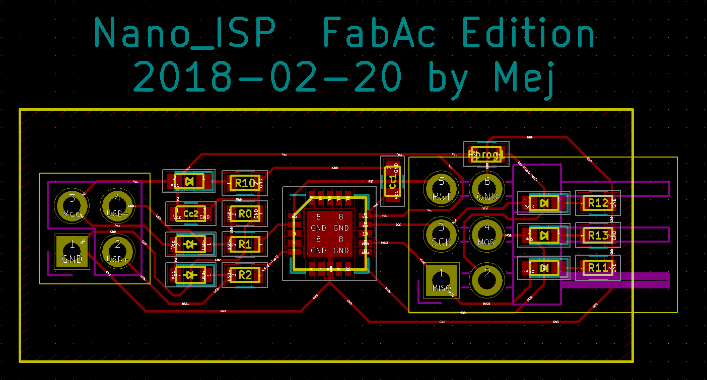
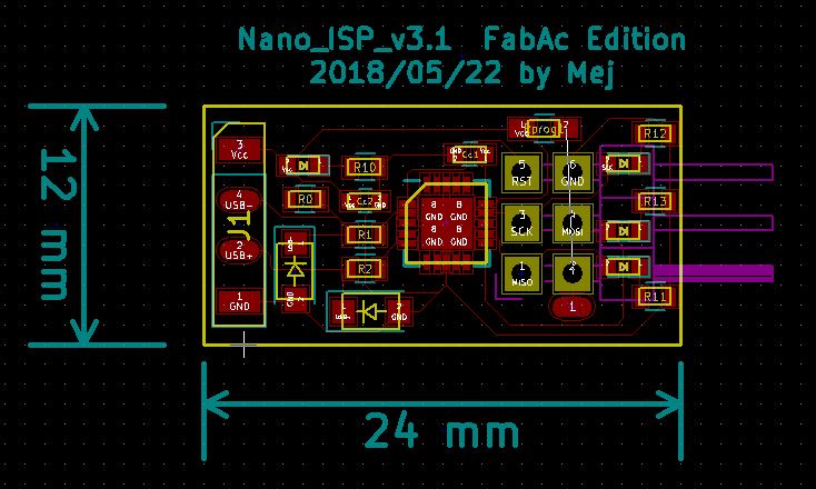
I copied and adapted the shematics of Brian in KiCAD.

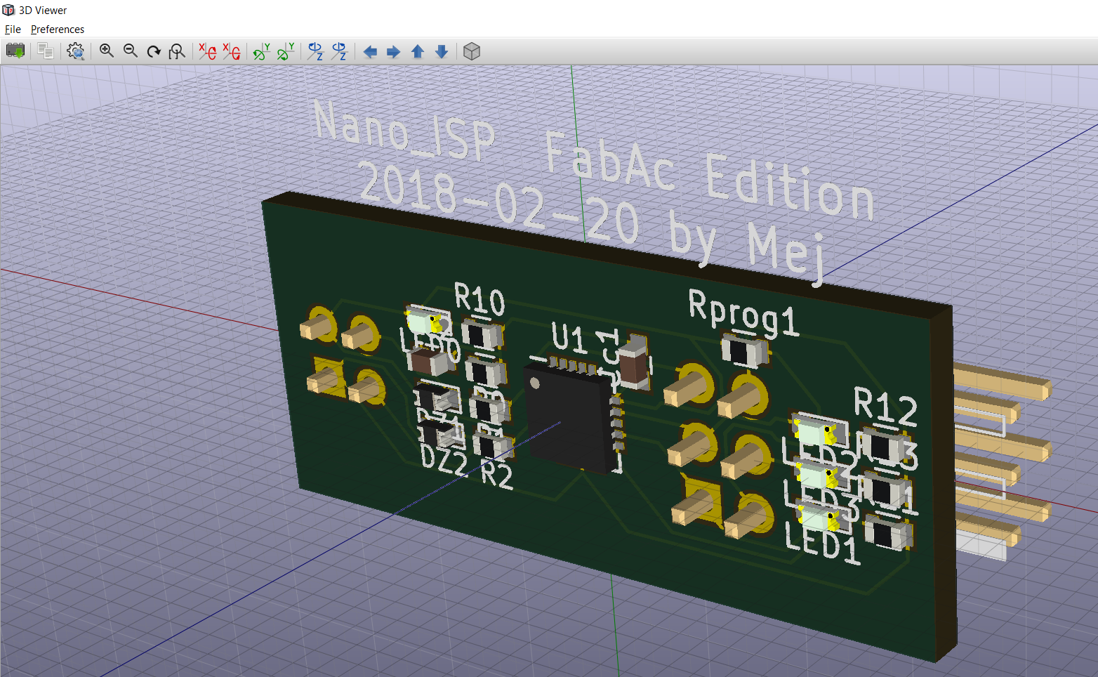
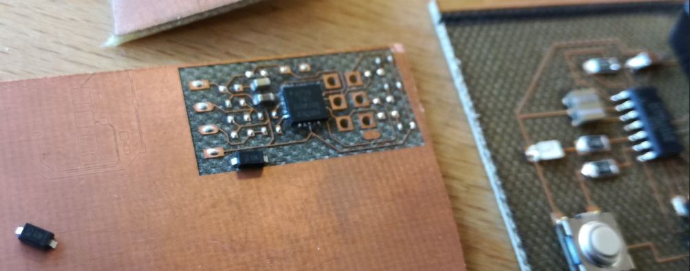
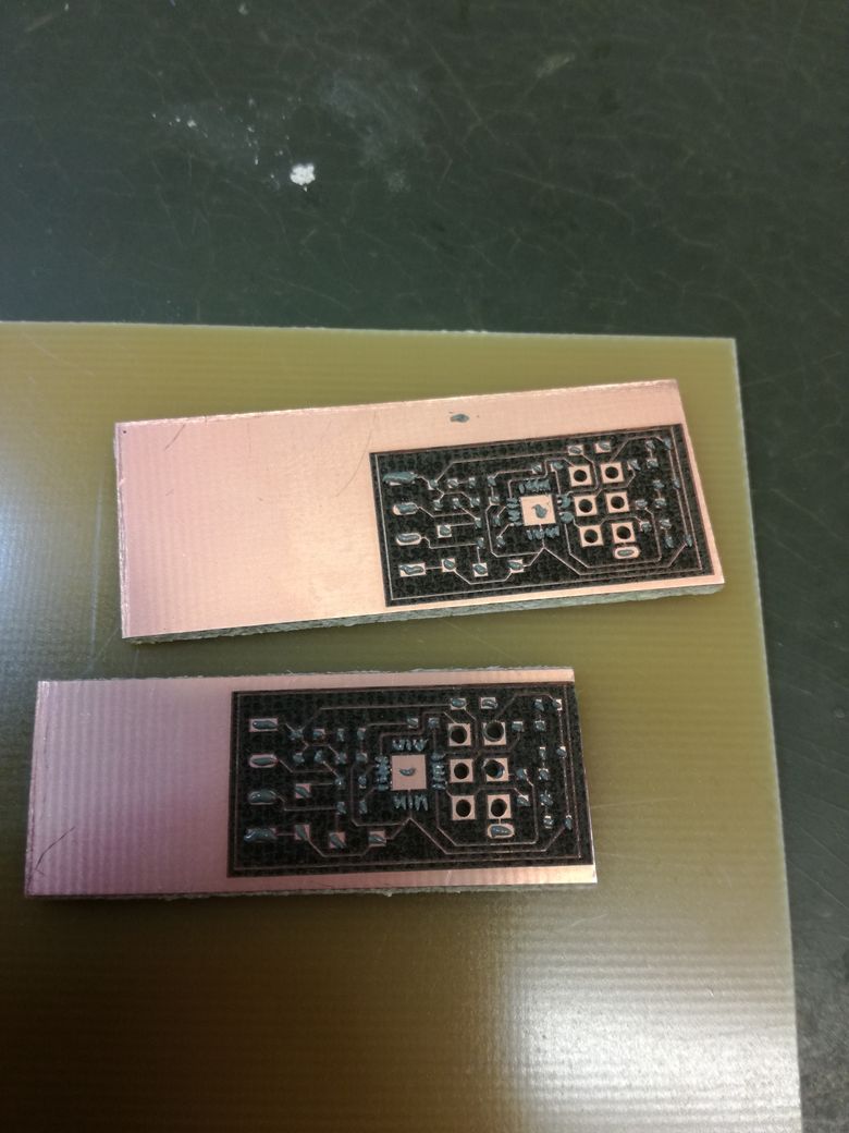
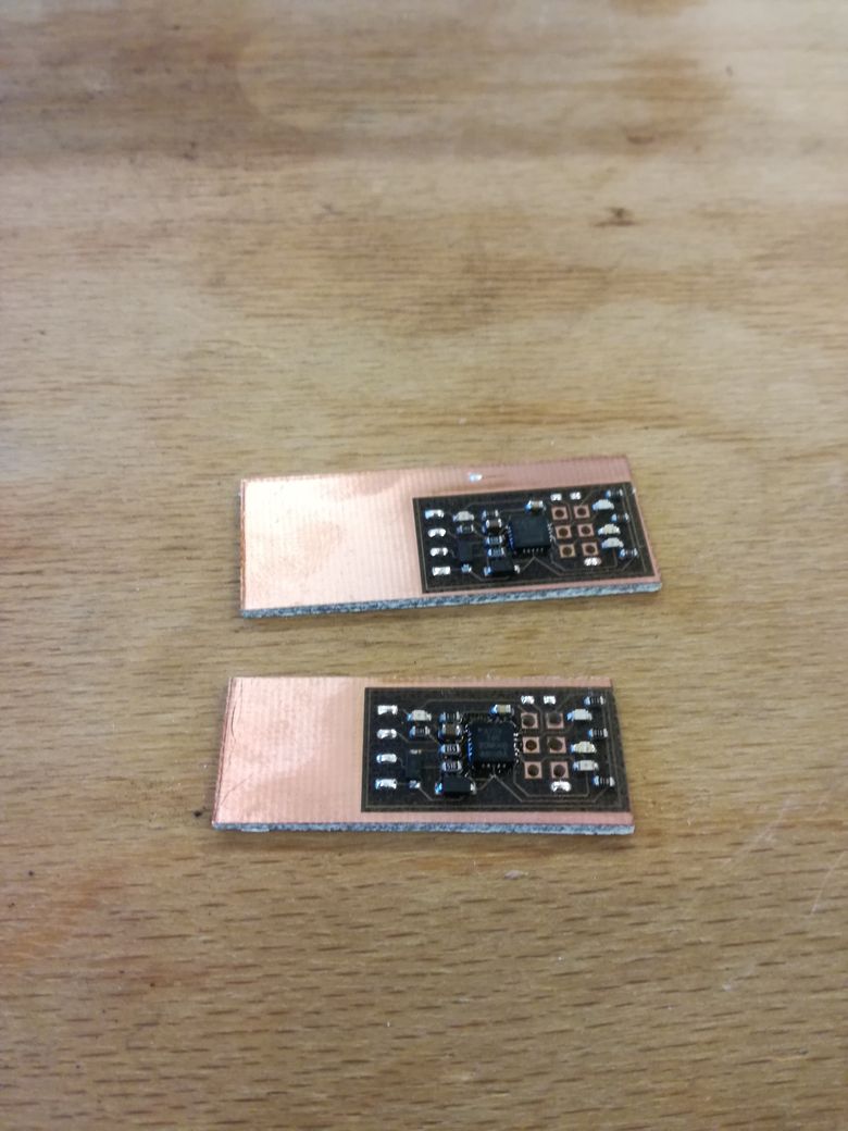
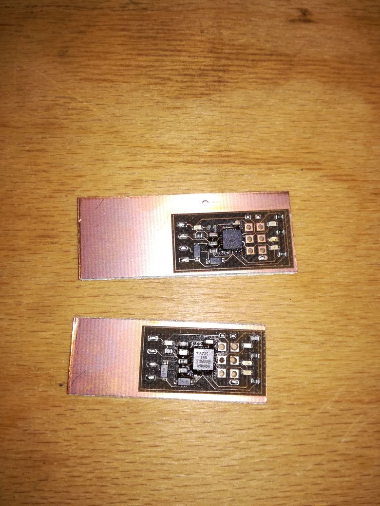
In my "Nano" version, all passive componants will be in package 0603 (1.6x0.8mm). The ATtiny 45 will be in QFN-20 (4x4mm). Nano size!

I will be using 4 LEDs: Orange, Red, Green and Blue for indicating activity of respectivelly Vcc, MISO, SCK and MOSI. Colorfull!

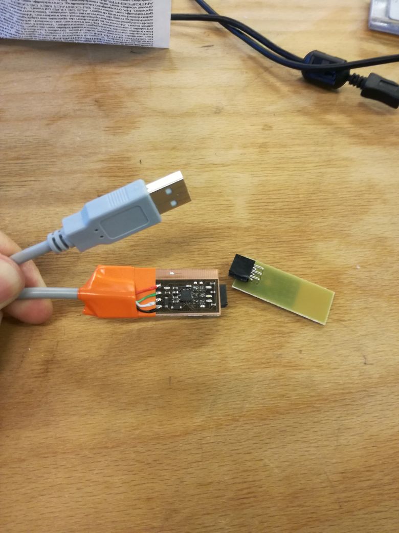
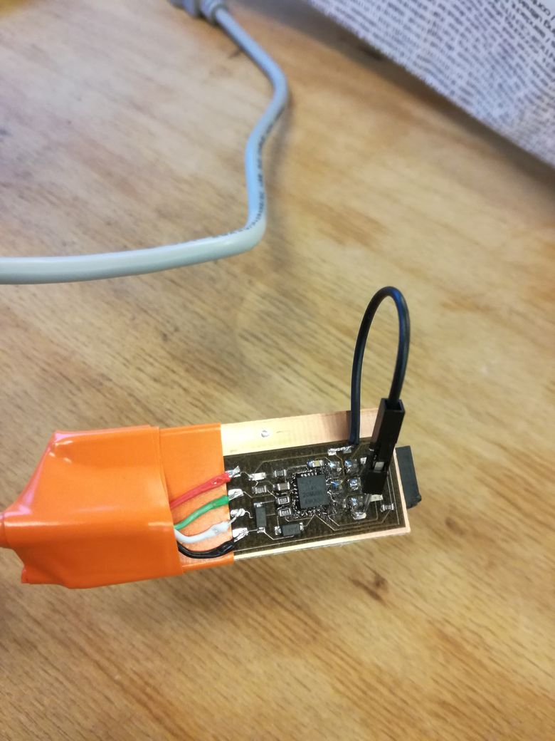
The "USB side" will be directly soldered to a USB cable. Ready to plug!

The "ISP side" will be a through-hole 90 degree pinhead. Linear shape!


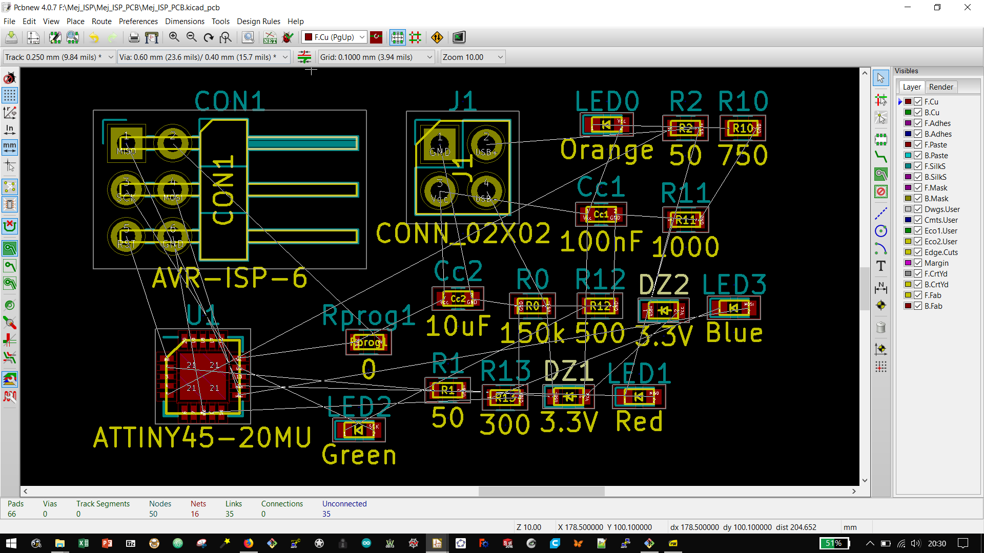
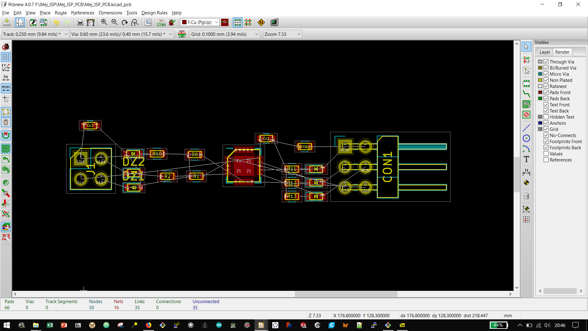
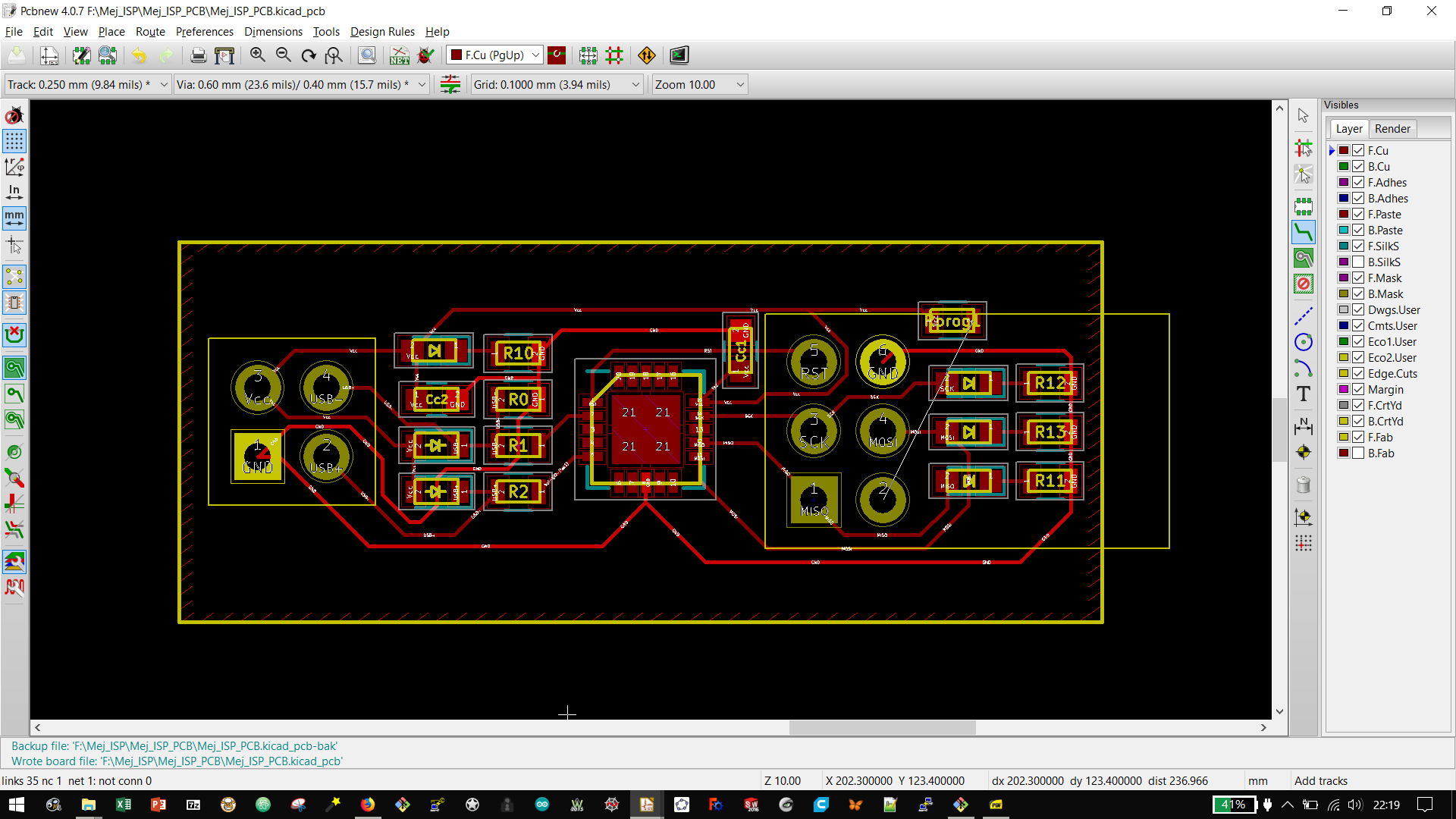
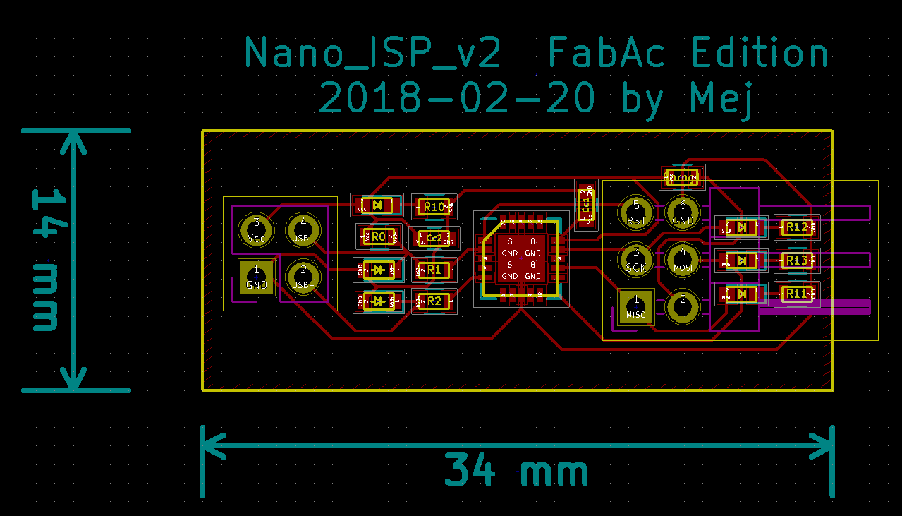
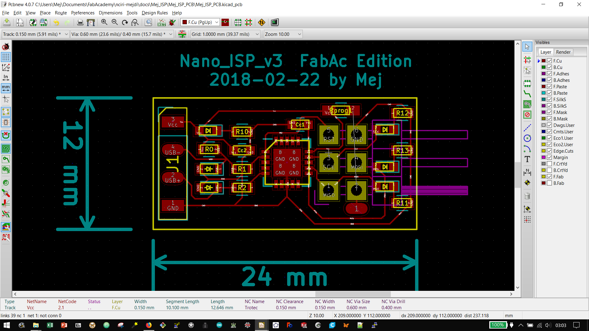
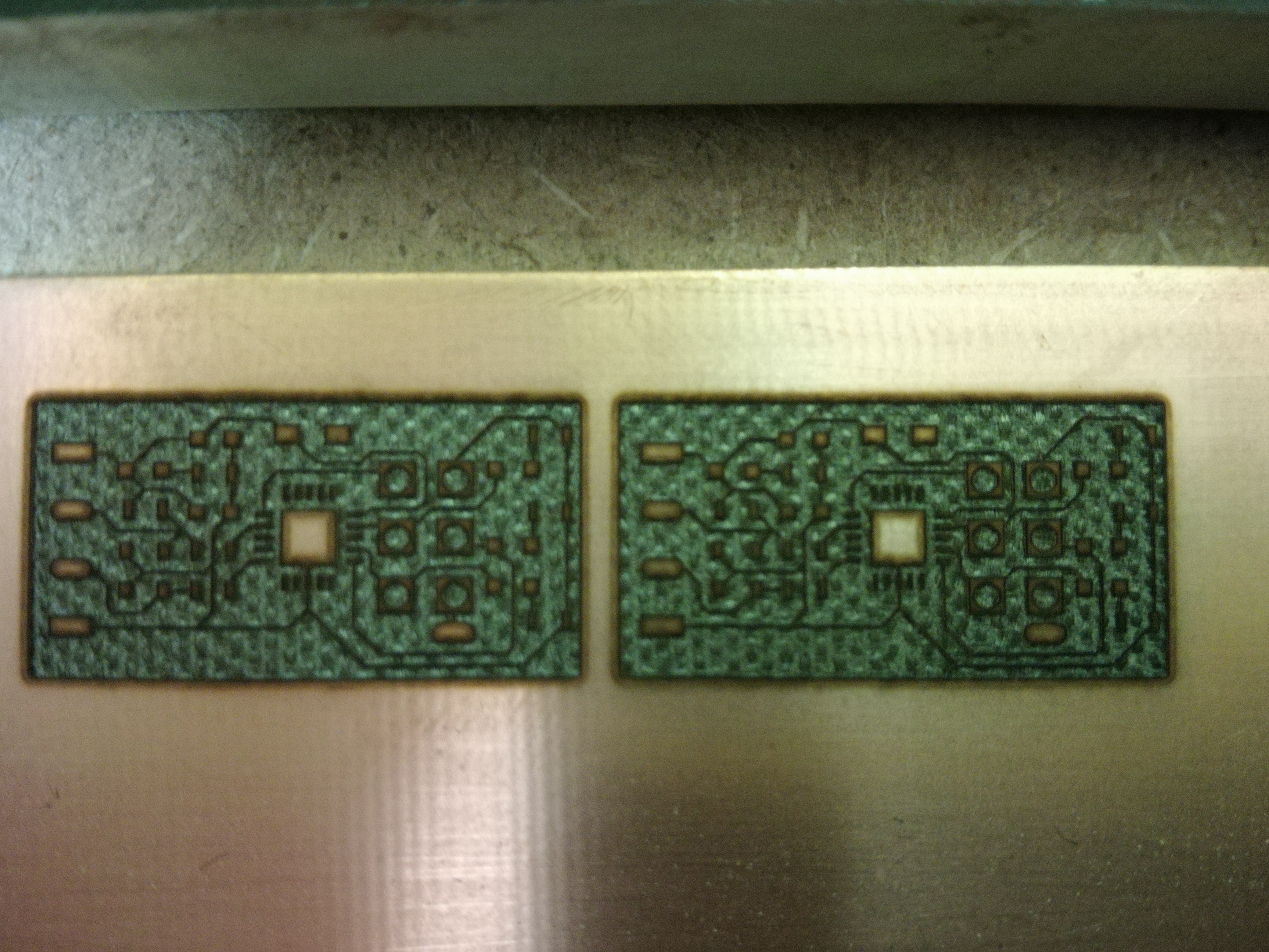
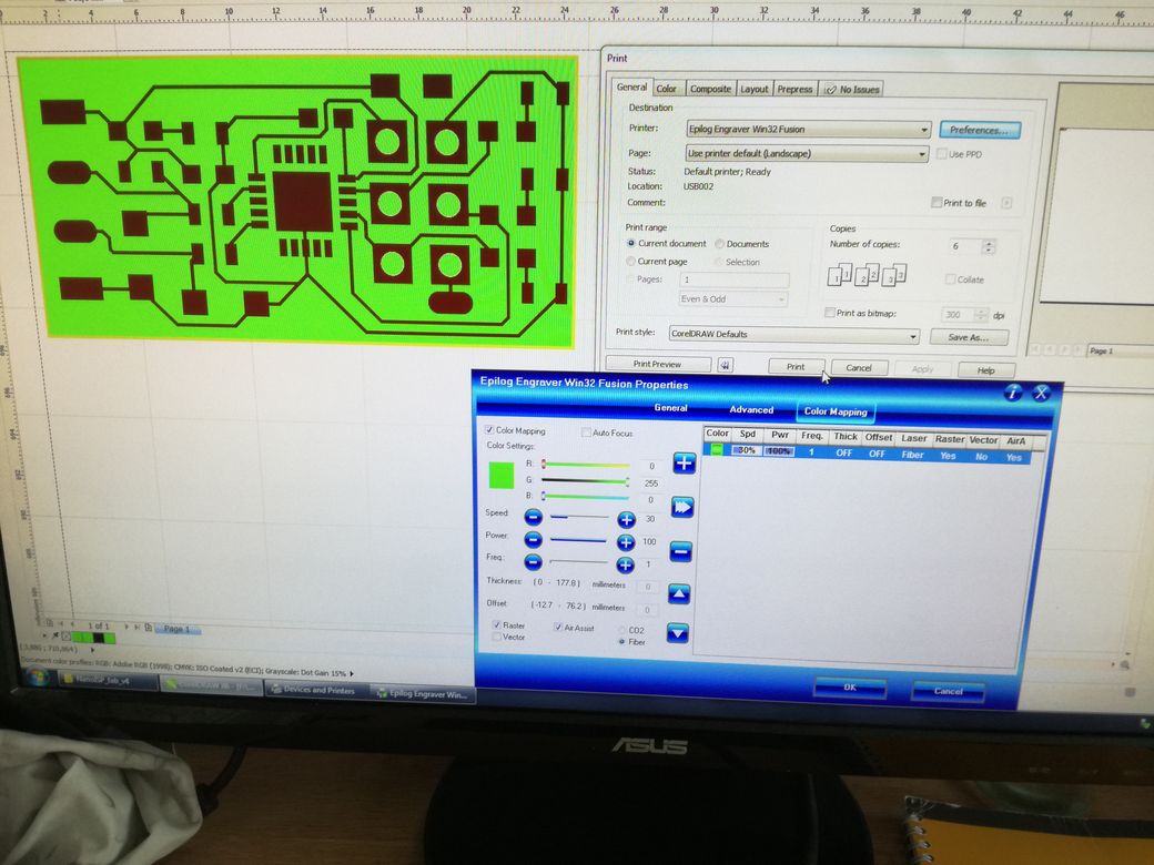
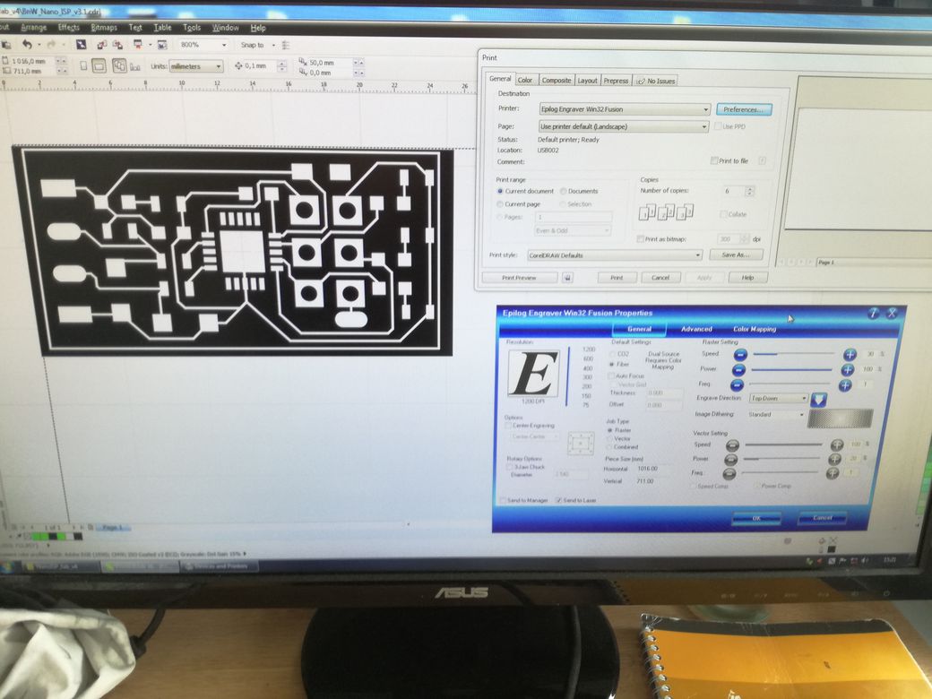
Then, I reduced the PCB to the "Nano" size of 12 x 25 mm (0.5 x 1 inch):

Source files

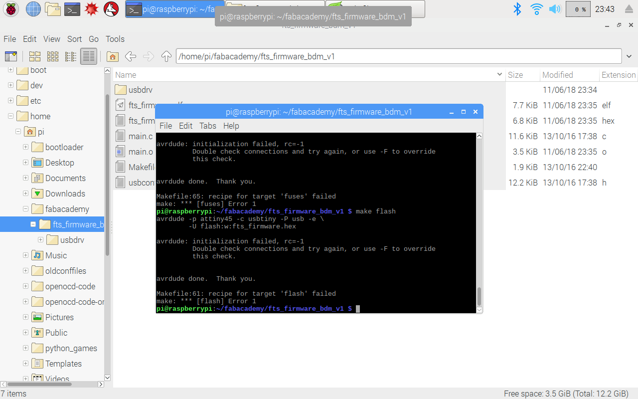
My source files can be found in this KiCAD project folder on gitlab.

The essential fabrication file are:


Production

After laser engraving using 503's Trotec:

When I tried to soldered, I realised that I had the wrong footprint for the Zener diodes. I used 0603, but they were SOD132.

I corrected the footprints:

I engraved using Digiscope's Epilogue. I investigated the "color-map" mode. But the CO2 laser was used in alternance with the Fibered laser... I tryed different advanced settings but couldnt fixe the bug. I went back to good old Black & White raster.


programming the Nano_ISP

With my RaspberryPI I followed the tuto of Brian. As a programmer I used a FabOptimus of the Digiscope.

Everything worked fine, but I couldn't see my Nano_ISP connected on the USB, using the lsusb command.
When doing tests, after many plug-unplug and reprogramming, I did a wirering mistake connecting my Nano_ISP to the FabOptimus (inverting GND and Vcc). I think I killed the ATtiny, because now I cannot even flash it :/


Back to Mejdi_FabAcademy_FollowUp