WEEK 12 - OUTPUT DEVICES
INTRODUCTION
This week we are required to design and develop a board to demonstrate output device where once we trigger an action we get a specific output. Since my final project is basically sending Infra-red signals, I decided to create a circuit where once I tigger a specific pulse, it sends out IR code.
Assignment Description
- Group Assignment: measure the power consumption of an output device
- Individual Assignment: Add an output device to a microcontroller board you've designed and program it to do something.
Learning Outcomes
- Demonstrate workflows used in circuit board design and fabrication.
- Implement and interpret programming protocols.
Have you (Checklist)
- ✔ Described your design and fabrication process using words/images/screenshots.
- ✔ Explained the programming process/es you used and how the microcontroller datasheet helped you.
- ✔ Explained problems and how you fixed them.
- ✔ Included original design files and code.
GROUP ASSIGNMENT:
The main requirement of this assignment is for us as a group to work collaboratively to test the power consumption of an output device, but before starting here are few definitions and information about electrical power:
POWER: is measured in watts, and is the energy available to do work. The formula to calculate power in watts is Power(watts) = Voltage X Current. A 20A 120V circuit theoretically has 2400 watts of power available.
OHM's LAW: states that the current through a conductor between two points is directly proportional to the voltage across the two points. V=(IR) where I is the current through the conductor in units of amperes, V is the voltage measured across the conductor in units of volts, and R is the resistance of the conductor in units of ohms
POWER CONSUMPTION of a device can be broken down into the continuous component – the amount of power a device always draws whenever it is turned on, sometimes called idle current, and the intermittent component – additional energy required when the device is doing work, such as lighting a lamp, or amplifying a signal to be sent to a loudspeaker. For Lighting systems, including both tungsten and LED, have a small continuous power requirement to operate the control circuitry and a comparatively large intermittent power requirement when the lamp is on.
Now the time came to answer the WHICH? WHY? HOW? WHAT? …
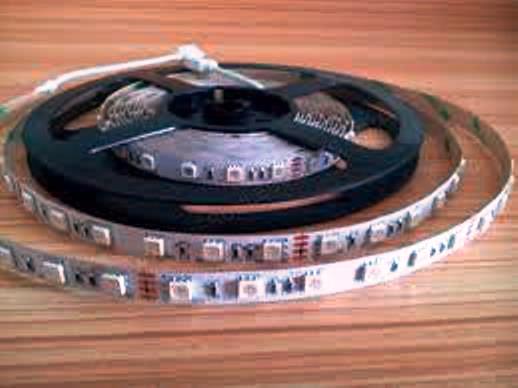
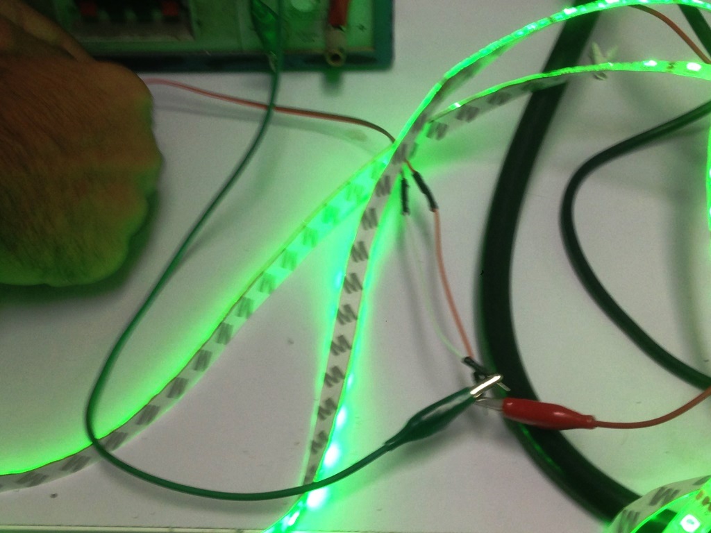
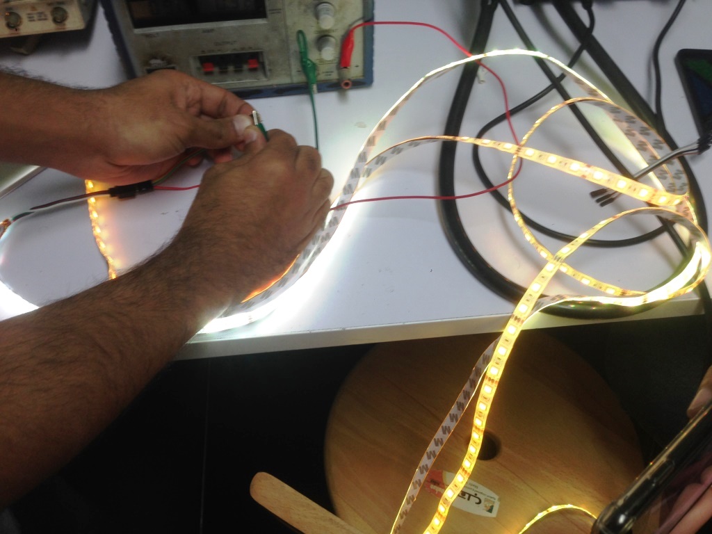
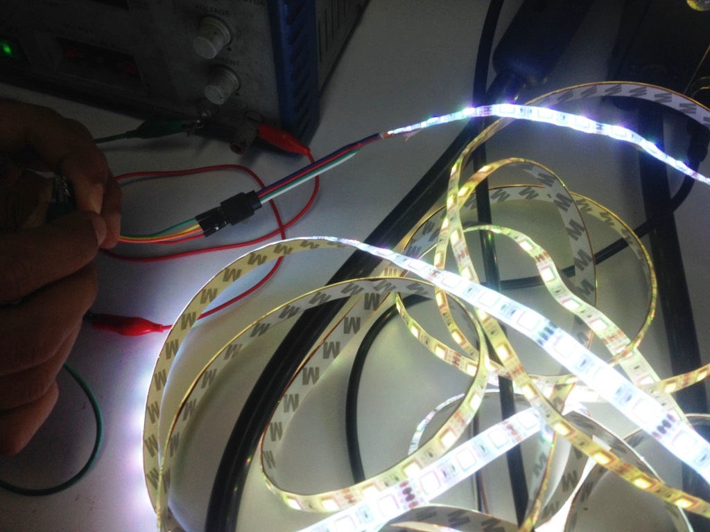
WHICH output device we should choose for our assignment? After thorough thinking we decided to test the power consumption of 5 meters RGB LED Strip (more information about the used LED Strip can be found HERE )
WHY we chose this output device? The main reasons we chose the RGB LED strip were:
- Convenience as it operates in different modes (i.e: Different colors RED, GREEN, BLUE and WHITE) and can accept different input voltages up to 12 volts accordingly will allow us to apply different voltages (in our case 9 volts and 12 volts) and measure the power consumption related to each.
- Easier to visually observe the outcome and the effect as not ONLY the readings of the drawn current in each case will be displayed on the power supply but also the LED color and brightness can be easily visually observed by eye.
- Safer to deal with as the output is DC not AC.
HOW did we measure the power consumption?
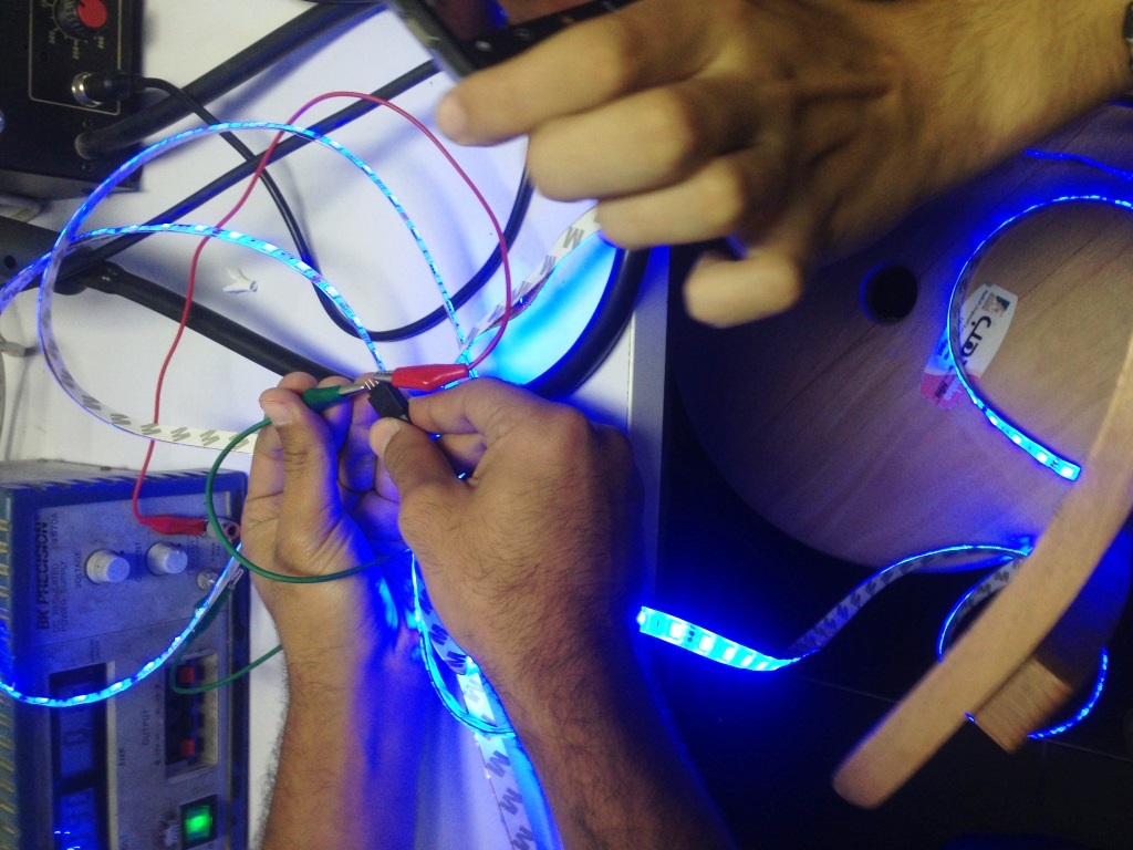
- We first removed the LED strip connector and we connected the 3 wires of each of the RGB LEDs and the GND to jumper wires.
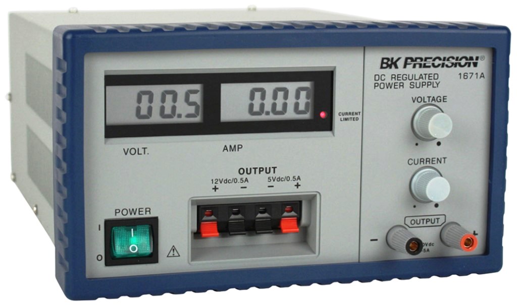
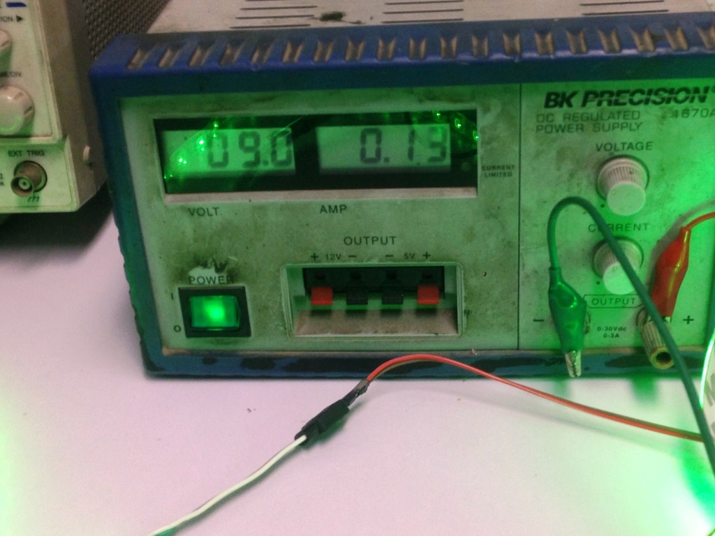
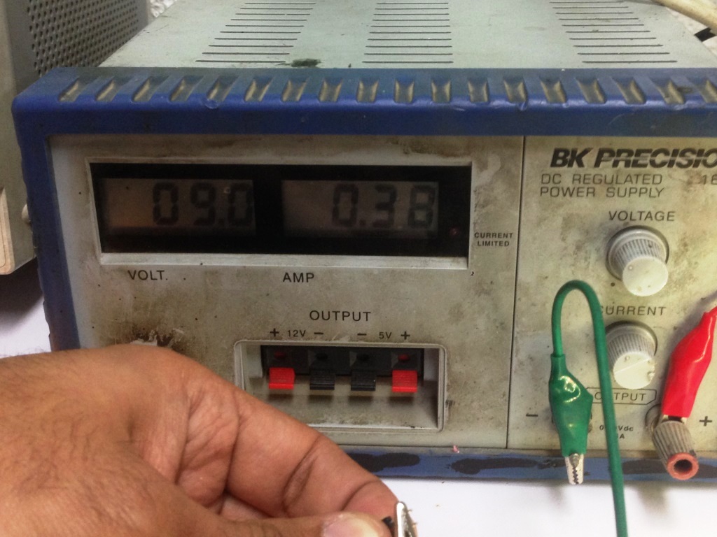
- We used an adjustable output AC-DC PSU (Power Supply Unit) and we fixed the output to 9 volts.
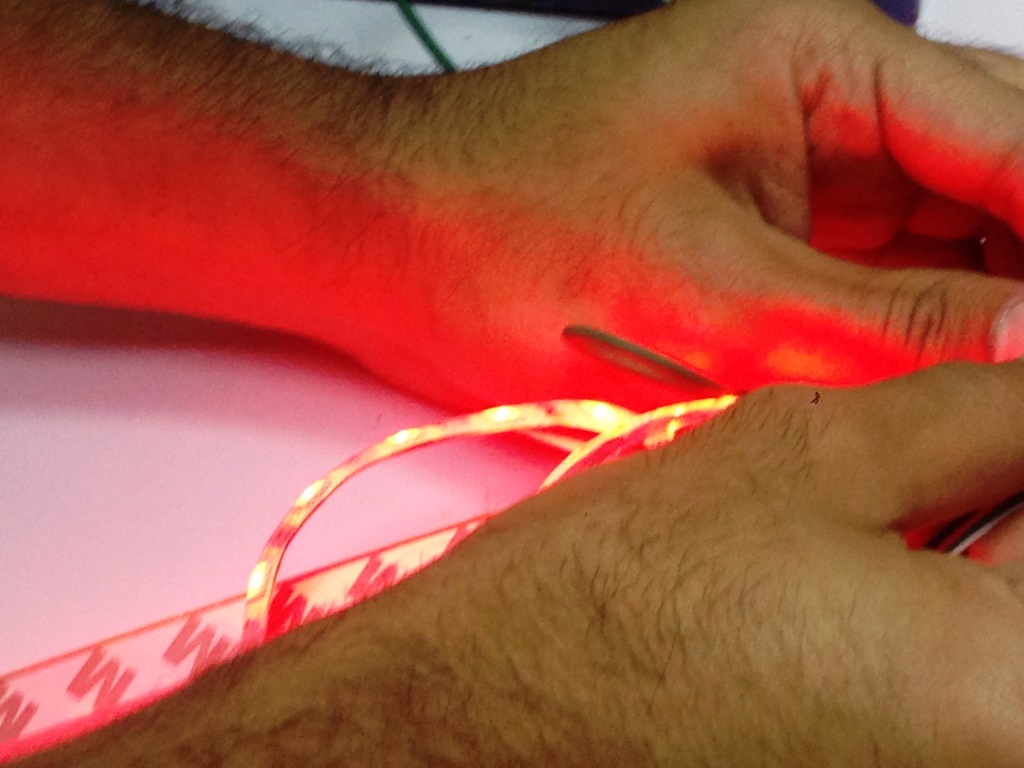
- We connected the RED LEDs jumper wire and the GND to the PSU and measured the drawn current.
- We performed the same steps with the GREEN LEDs, BLUE LEDs and finally connecting ALL the LEDs jumpers simultaneously to the PSU.
- We recorded the outcomes and the results are as follows:
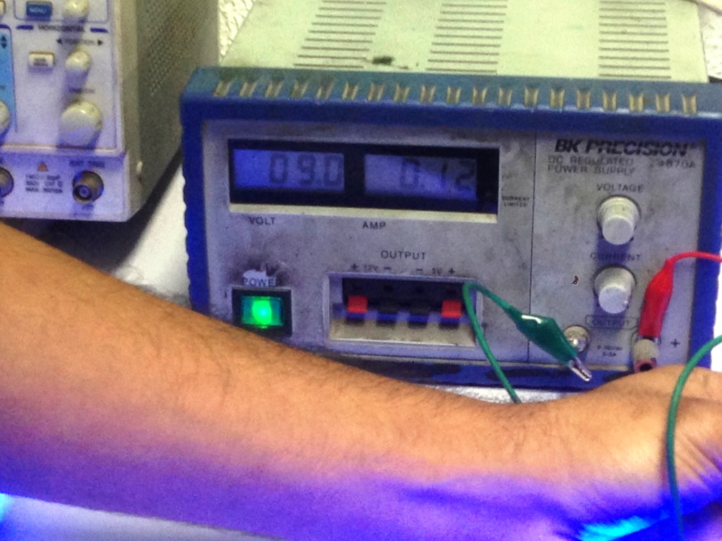
- At 9 Volts - Blue LED Current = 0.12 Amps
- At 9 Volts - Green LED Current = 0.13 Amps
- At 9 Volts - RED LED Current = 0.34 Amps
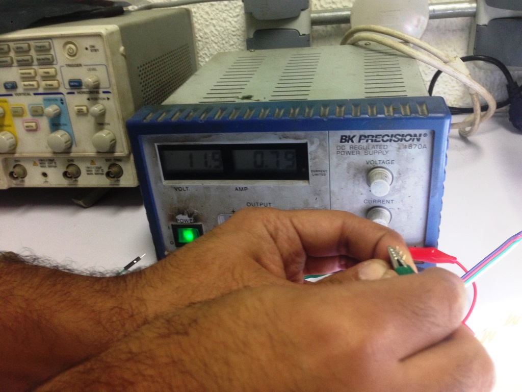
- We changed the adjusted voltage in the PSU to be 12 volts (The maximum that the LEDs strip can take and we repeated the previous 3 steps and the recorded results are as follows:
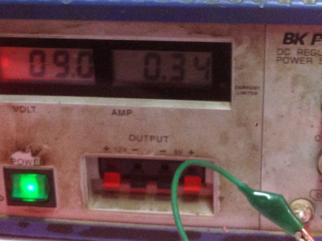
- We changed the adjusted voltage in the PSU to be 12 volts (The maximum that the LEDs strip can take and we repeated the previous 3 steps and the recorded results.
WHAT are the findings??
- The current drawn for the RED LED is the highest each time. Which implies that the resistance for the xyz LED is the lowest.
- Since the resistance in each LED is constant, when we apply higher voltage higher current flows in the LEDs (Refer to OHM’s Law: V = IR).
- The LED’s brightness is directly proportional to the current that flows in the LED’s strip.
- Since the LED’s distribution in the strip is uniform, so is the resistance as well. Accordingly, The power consumption in the strip is directly proportional to the length of the strip (i.e: The less the length of the LED Strip the less the power) consumption.
INDIVIDUAL ASSIGNMENT:
TOOLS AND HARDWARE USED: (COMPONENTS)
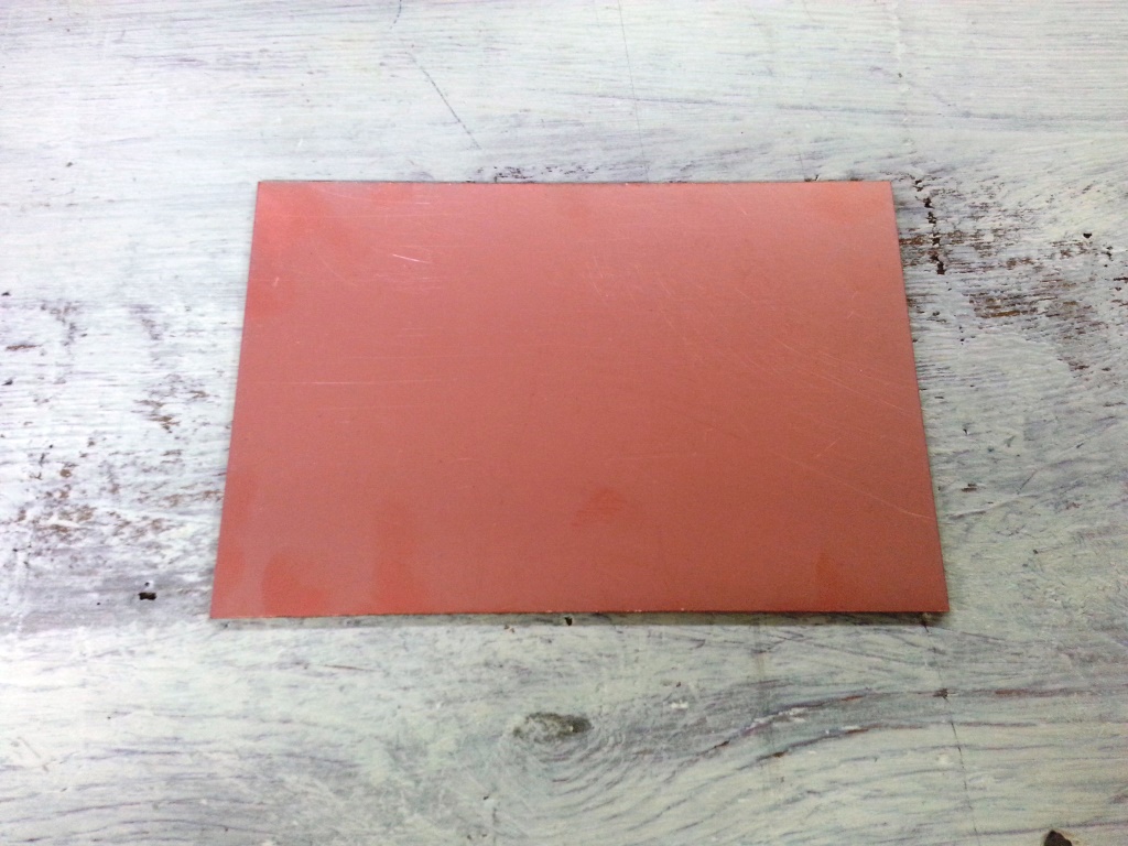
- 1 x FR1 (Copper PCB Board).
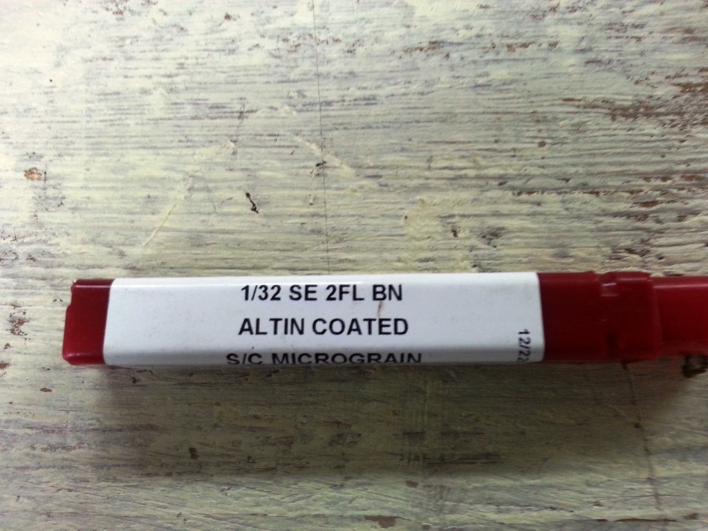
- 1 x 1/64 inch end mill bit.
- 1 x 1/32 inch end mill bit.
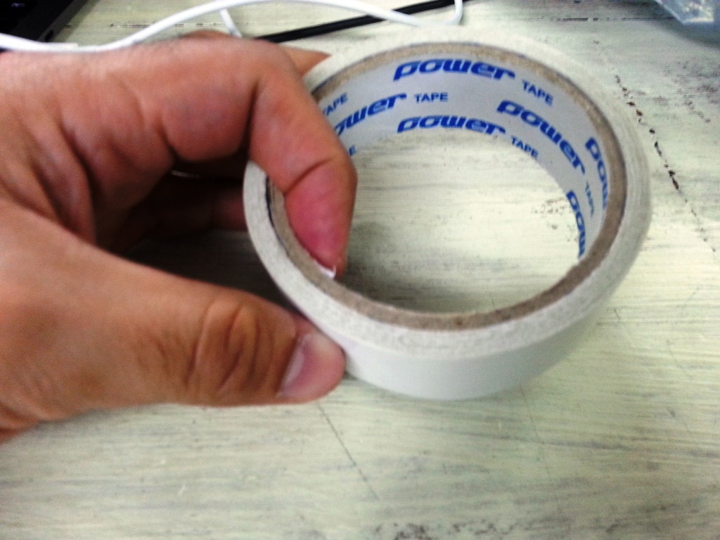
- 1 x double tape.
- 1 x Modela MDX-20 (More about the Machine can be found in THIS LINK
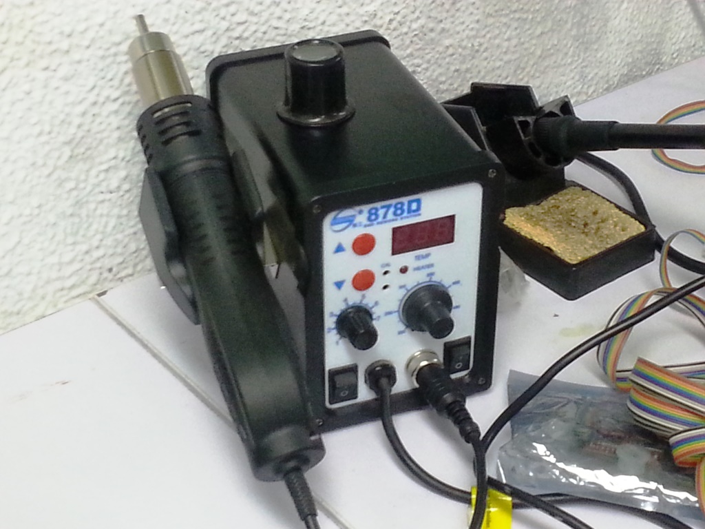
- 1 x Soldering Station.
- soldering wire
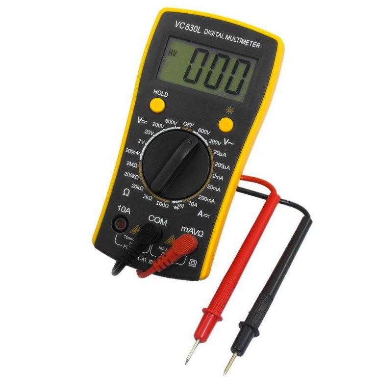
- AVO multimeter
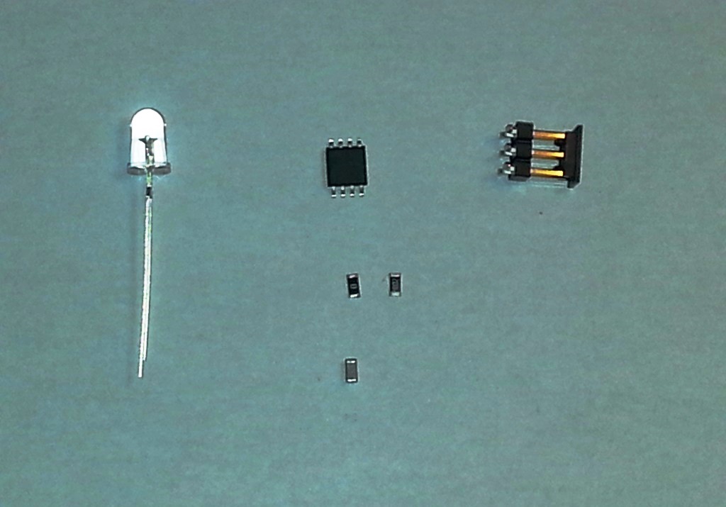
- Electronic Components Including:
- 1 x ATTiny45-SSU.
- 1 x (2x3) pin header for AVRISP
- 1 x (1x6)pinheader for Rx,Tx,VCC,GND
- 1 x IR LED.
- 1 x 1 uF Capacitor.
- 2 x 10k Resistor
- 1 x 499 Resistor.
STEPS PERFORMED:
CIRCUIT DESIGN
- I decided to use Autodesk Eagle as a CAD tool to design the circuit, I followed the same steps that I performed in WEEK 7 electronic design assignment.
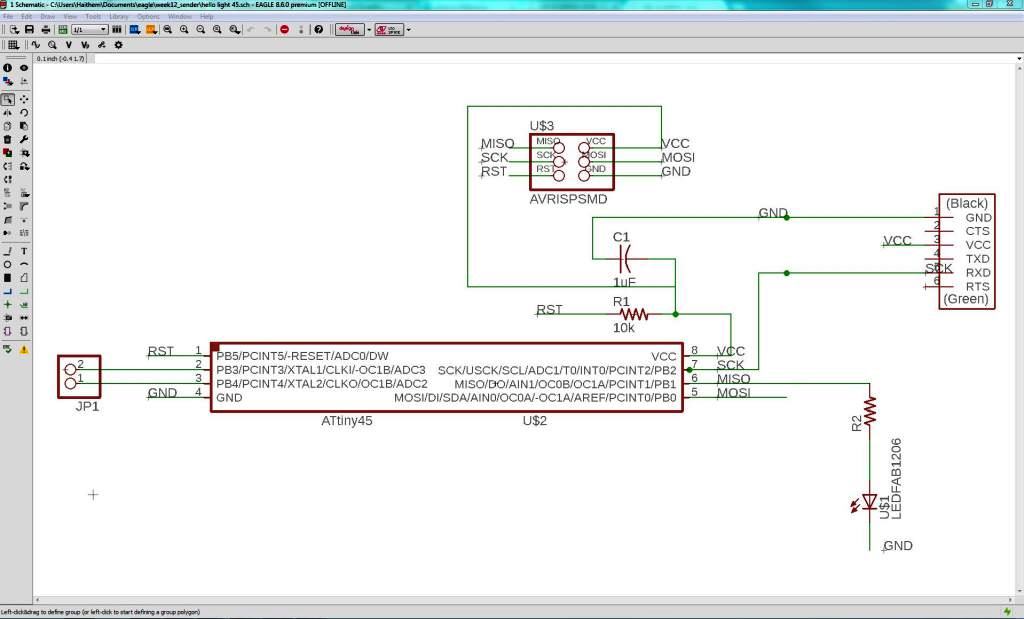
- I opened the board that I created in WEEK 11 and I started to modify it and I performed the following modifications:
- I removed the photo-transistor and the 10 K resistor connected to it.
- I added an IR LED to the ATTINY45 Physical PIN6 with a 499 Ohm resistor from one side and the ground from the other side.
- I added 2x1 PIN male-header to use them for getting RX and TX from other boards.
JUSTIFICATION: I wanted wider angle for my IR and accordingly I decided t use the through-hole IR led, I still wanted my board to work with SMD as well if I needed to so I created the Pads for the LED component and I added a hole in it during the milling.
- I then switched to the board view by going to the top menu > File > switch to board. The board view will open up and components we just added will appear
- Use "move" to move each component around and "route" to route each trace. The wire will turn red as you route it into place.
- Keep moving and adjusting the wires and components till you reach the final desired layout as shown below.
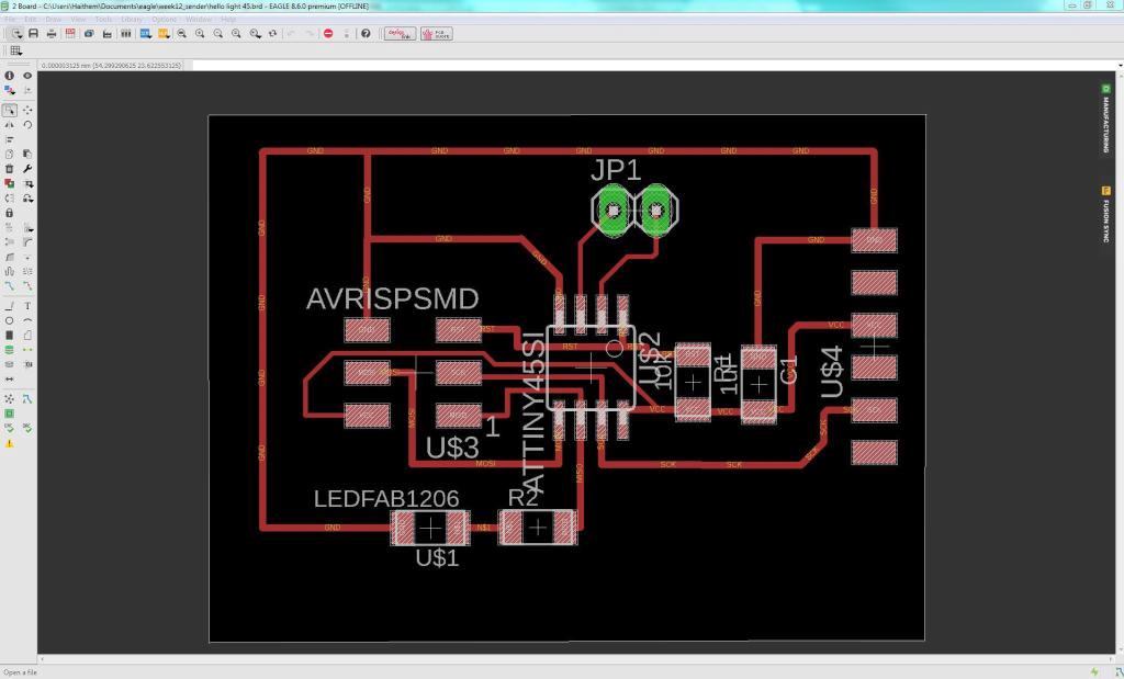
- After I finished the orientation and wiring the components in the board view I started to do the design check also known as DRC. the main purpose of te DRC is to ensure that the used 1/64 inch mill-bit tool will have enough clearance to mill around the traces and in-between them.
- a mill-bit with the diameter of 1/46 inch (~16 mil) is used; So I opened the DRC from The "Tools" menu. Then in the "Clearance" tab, I wrote "16mil" to all the fields there.

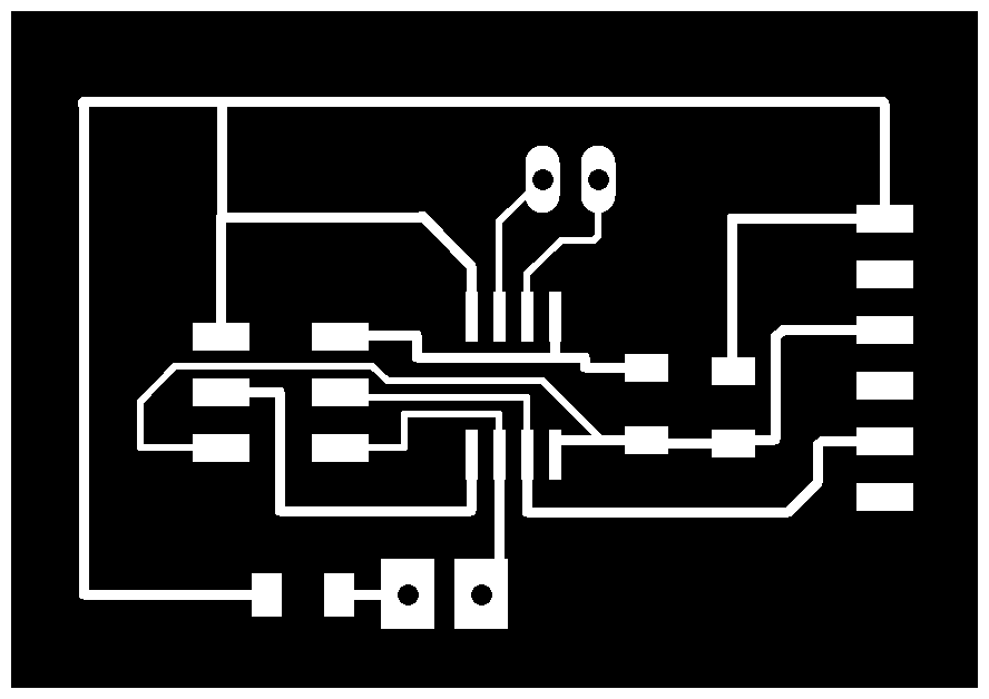
- Finally I started to export the circuit to PNG image and I edited them using GIMP to create the TRACES PNG FILE and BORDERS PNG FILE and I performed the following steps:
- I opened GIMP, I opened the file I exported from Eagle and then I used the "Rectangle Select" tool, I selected the inner border of the dimension rectangle and then right-click->Image->Crop To Selection.
- To add a border, I clicked Image->Canvas Size and added 20px to width and height and the clicked on the "Center" button. Then to make the border white, I clicked Image->Flatten Image. Then saved the image.
- I created a new layer and I copied to it all the through-hole circles.
- In the main layer I used the "Bucket Fill Tool", I blackened all the traces so that I'm left with only a white border and I inverted the color to get white borders.
- I went back to the layer where I created through-hole circle and I colored them whith black color.
- I exported the created files as PNG, Now we are ready for milling.

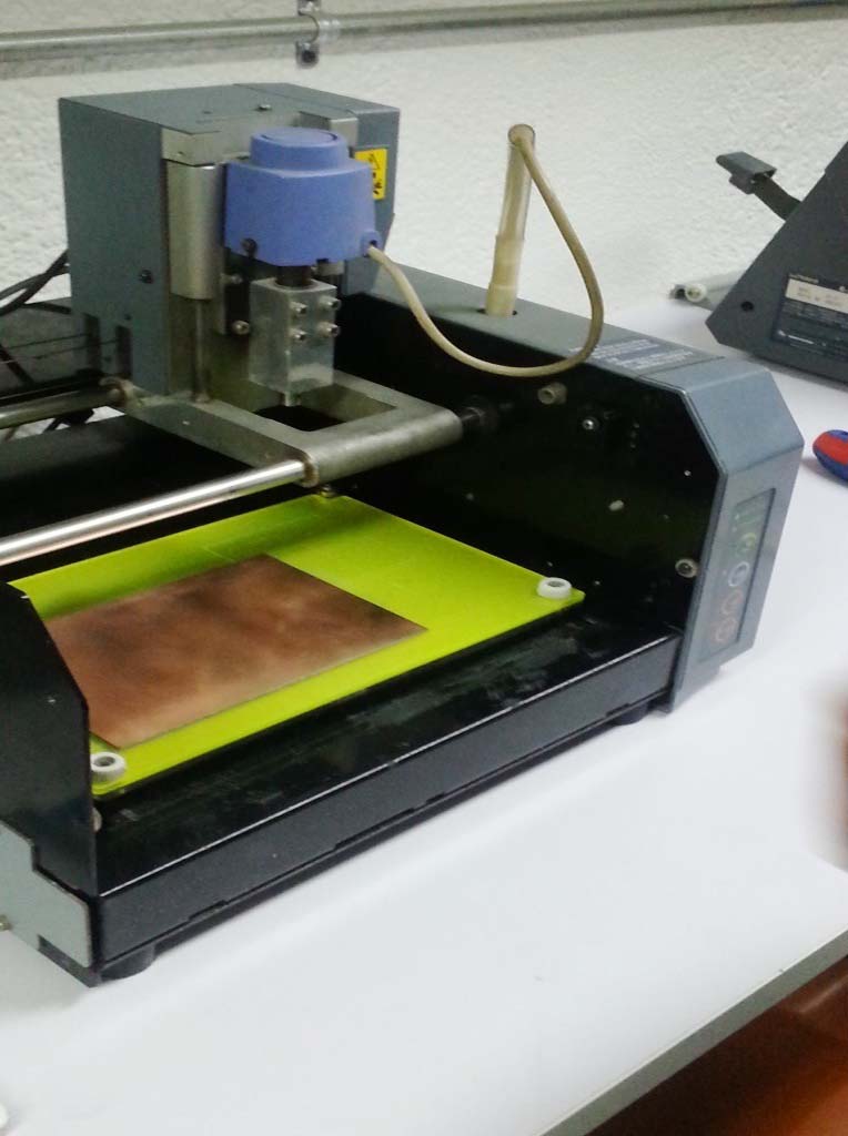
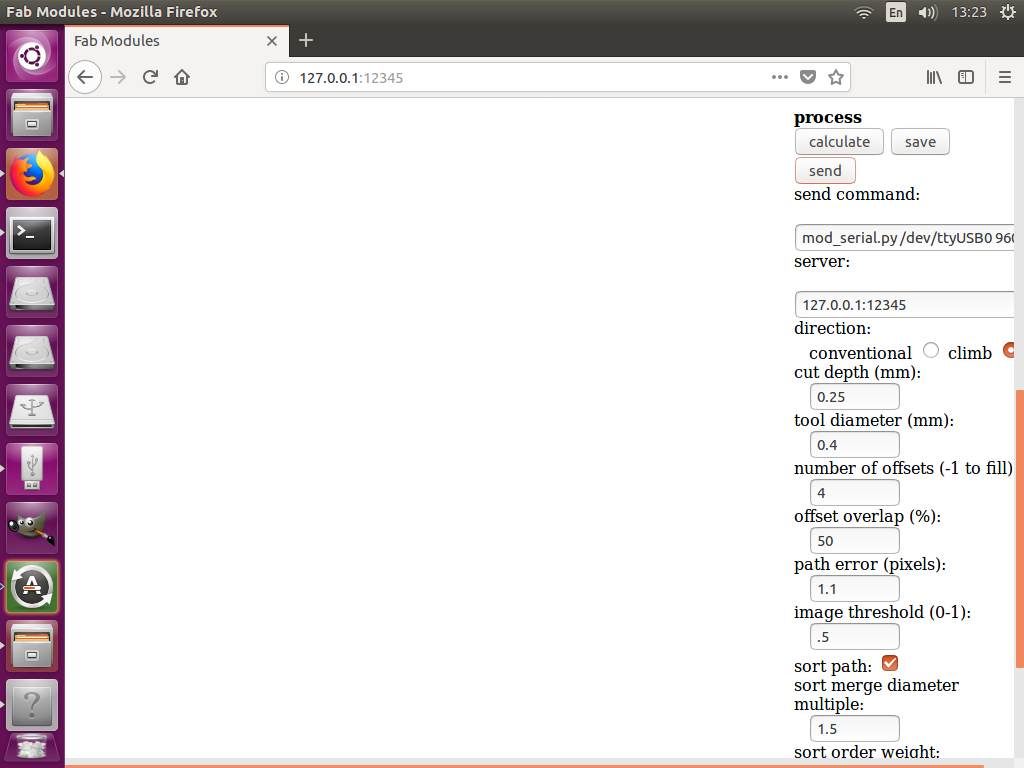
MILLING THE CIRCUIT
- I started milling the circuit PCB board on the Modela MDX-20 using Fabmodules and soldering the components follwoing the same principles we learned in WEEK 5
- For milling the traces:
- I used the 1/64 inch diameter end mill
- cutting depth = 0.25 mm
- number of offsets = 4
- For milling the borders:
- I used the 1/32 inch diameter end mill
- cutting depth = 0.25 mm
- cutting depth = 0.6 mm
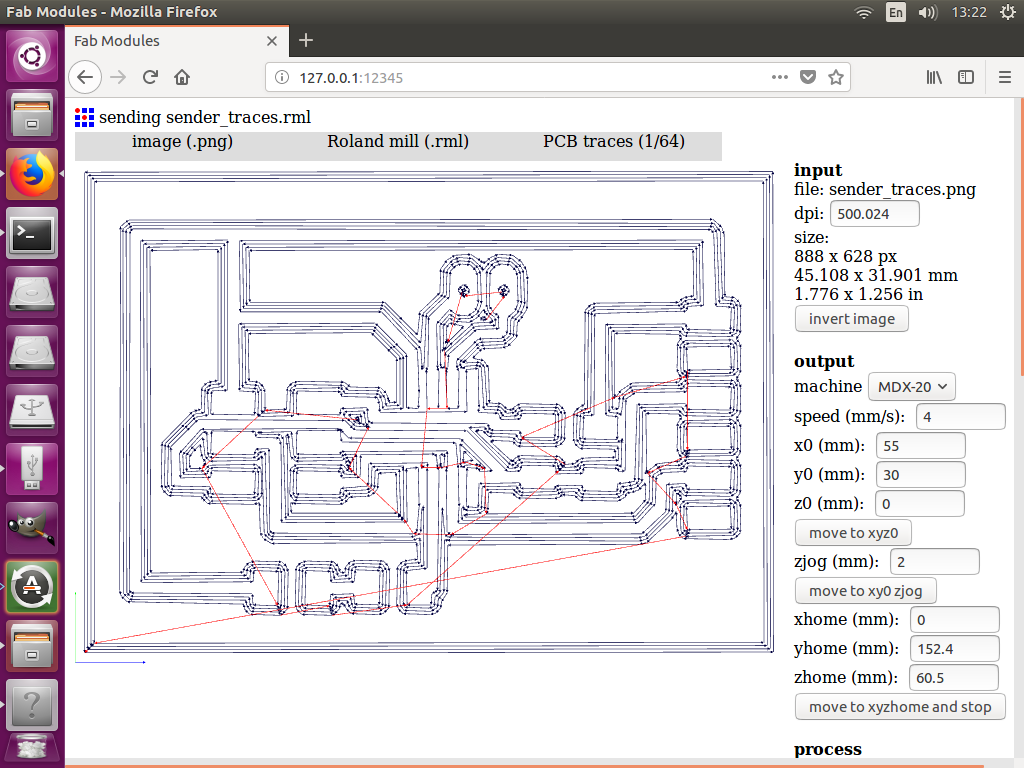
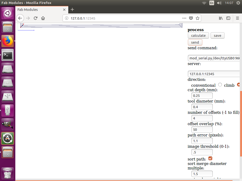
- I then started the milling as shown in hte video below
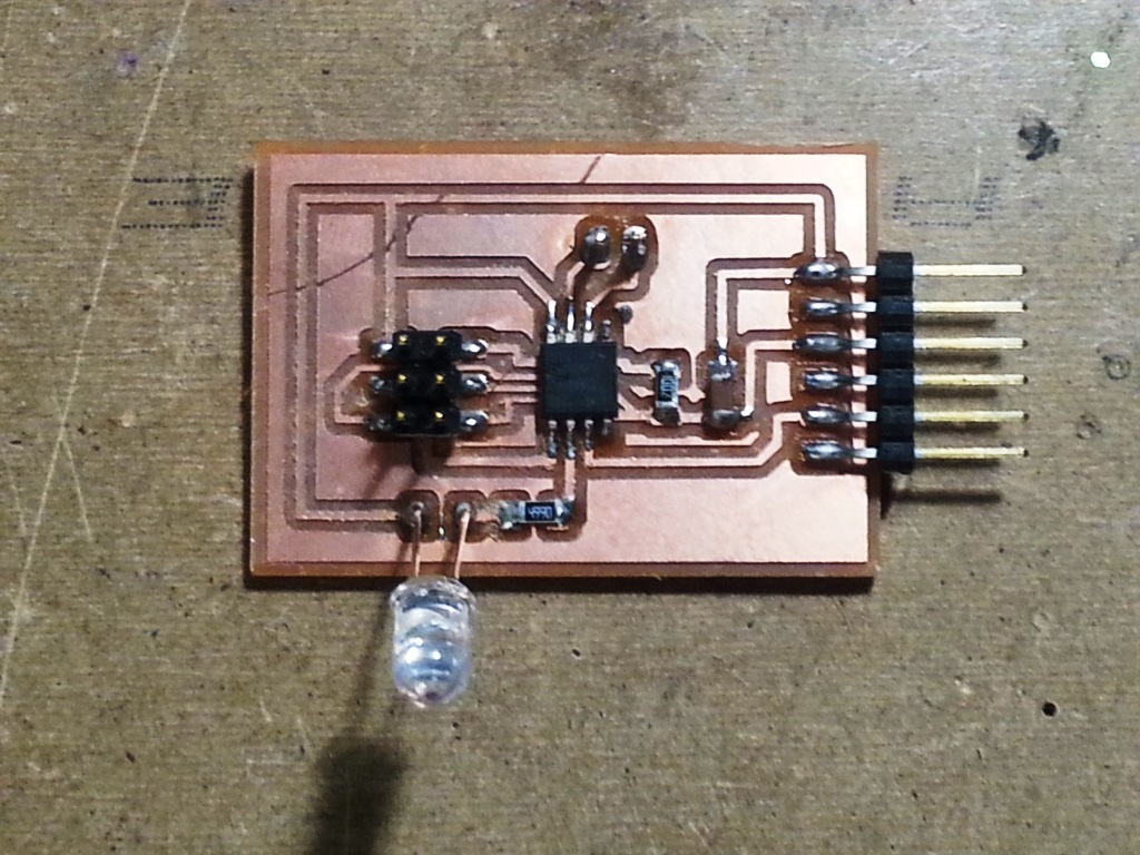
- When I created my board, I soldered the electronic components in the PCB circuit as shown below
CIRCUIT PROGRAMMING
PROGRAMMING USING ARDUINO IDE AND FABISP AS A PROGRAMMER
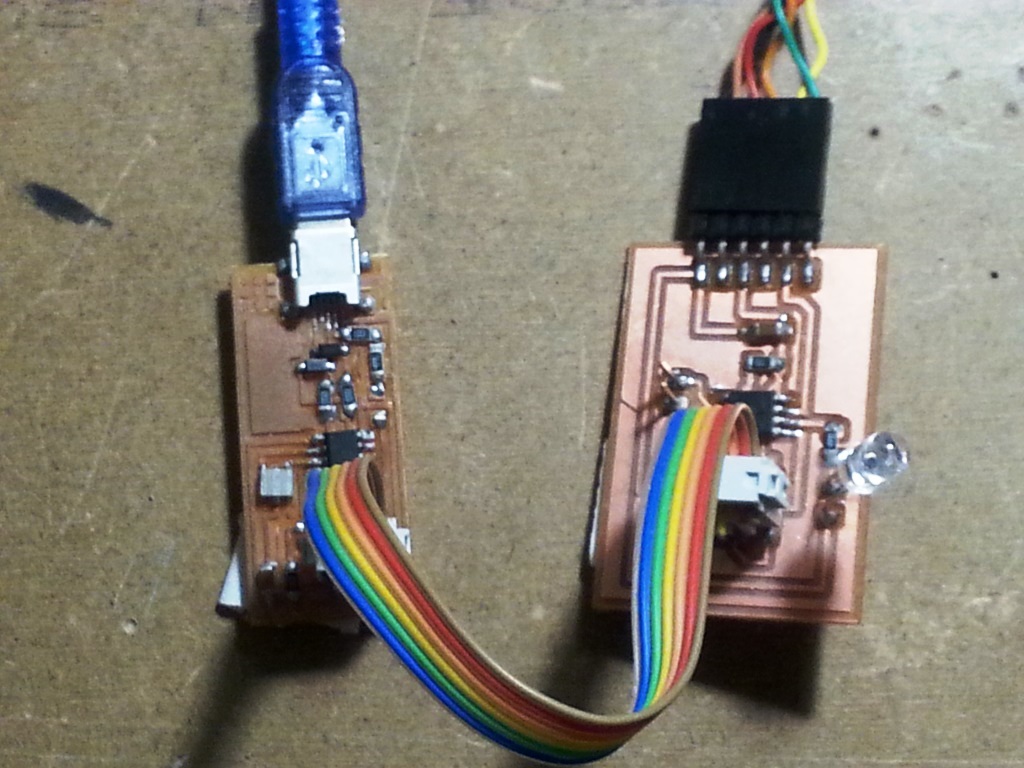
- Connect the FAB ISP pins to my board pins with each pin connected to its corresponding similar pin as follows:
- MISO (in FAB ISP) -> MISO (in IR-Emmiter Board)
- MOSI (in FAB ISP) -> MOSI (in IR-Emmiter Board)
- SCK (in FAB ISP) -> SCK (in IR-Emmiter Board)
- Vcc (in FAB ISP) -> Vcc (in IR-Emmiter Board)
- GND (in FAB ISP) -> GND (in IR-Emmiter Board)
- RST (in FAB ISP) -> RST (in IR-Emmiter Board)
- Connect the FAB ISP to the usb Port and ensure it is detected by the PC.
- Connect the FTDI Cable to the FTDI header in the FTDI pins in the IR-Emmiter Board.
- open arduino IDE then burn the BOOTLOADER.
- To burn the BOOTLOADER I followed the following steps:
- Select "USBTinyISP" under Tools > Programmer.
- Select ATtiny from Tools > Board.
- Select the specific ATtiny you are using (44/45/84/85) from Tools > Processor.
- Next select "16 MHz (INTERNAL)" from Tools > Clock.
- select "Burn Bootloader" under tools and wait till it complete.
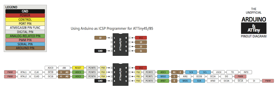
- I looked at the ATTINY45 Datasheet and the PINOUT map in the diagram below to identify the ARDUINO mapping of the Attiny45 pins
- I wanted to test that the IR is working and so I opened arduino IDE FILE -> EXAMPLES -> BLINK sketch, I modified the PIN 13 where the LED is supposed to be connected to be 1 and I uploaded the code.
- I opened the camera in my mobile and I saw the IR Emitter Blink (notice that you can not see that blinking with your eye and in some mobiles the IR is filtered so you might not be able to see it too)
- I wrote the following code and below are few notes about the code.
- I chose ATTINY45 Physical PIN 6 (Mapped to ARDUINO PIN 1) to be connected to my IR Emmiter
- I ONLY needed TX from my ATTINY to the FTDI cable to get messages from the ATTIN85, so I connected the ATTINY45 Physical PIN 7 (Mapped to ARDUINO PIN 2) to the FTDI RX PIN.
- To enable the board to be conected to another board and get the commands from it via serial port, I created pin headers at Physical PIN PB4 (to act as TX) and PB3 (to act as RX)
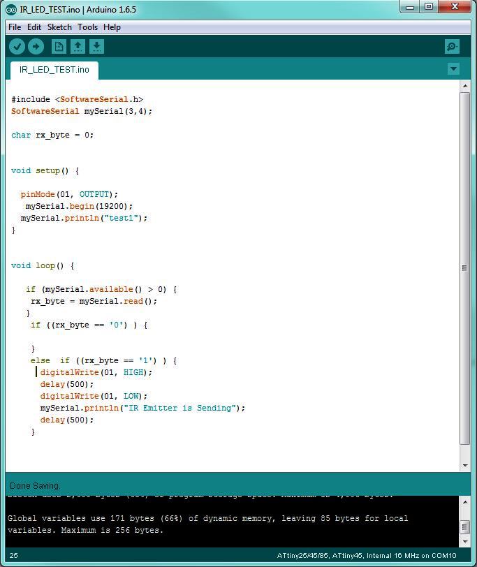
- I compiled the code then uploaded it.
- Whenever the number 0 is input in the serial monitor, the IR Emitter stops blinking, and when we input number 1 the IR Emmiter starts blinking again.
- The final result is as shown in the video file below.
OTHER OUTPUT BOARD (AS PER THE GLOBAL EVALUATOR REQUEST):
WHY TO ADD THIS SECTION?: My Global Evaluation had a comment coming from Francisco (My global Evaluator), who kindly draw my attention that blinking a LED (Even if it is an IR LED) does not add much to the skills I learned in the previous weeks and I can do more and create an output board that I did not create before. I valued Francisco's feedback and since I finished my Final project Early. I decided to get busy and do additional board ... If you are a student and reading this, then trust me you will keep learning till the last minute and this is the beauty of this diploma!!
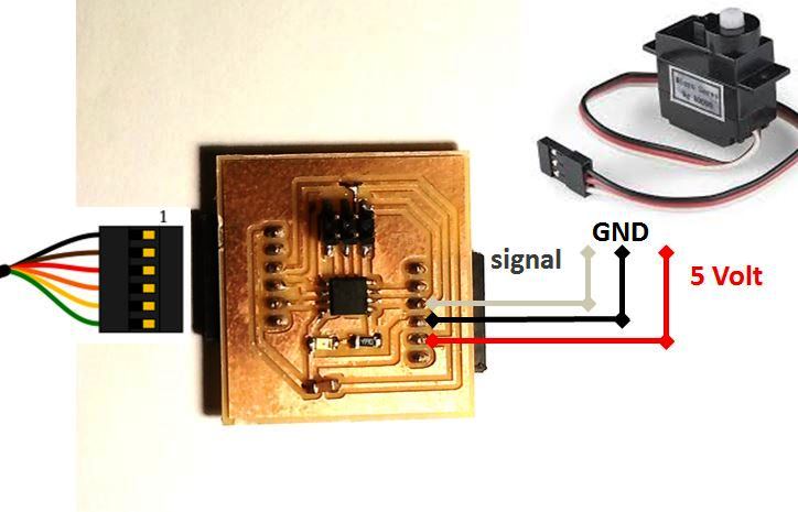
- I decided to work on a SERVO Motor and in order not to re-invent the wheel, I used the PCB that I created in THIS WEEK
- I connected the Servo to the board as per the diagram below:
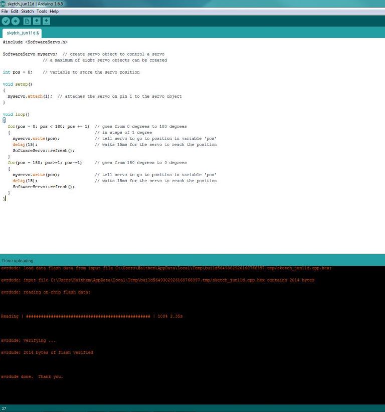
- I then did some investigations and I discovered that hte normal SERVO library will not work with my ATTINY45 and that the replacement is a library named "SOFTWARE SERVO LIBRARY", I downloaded it from THIS PAGE and I installed the library.
- I connected the attiny45 to the FABISP and burnt the booatloader ( I configered the clock as INTERNAL 8Mhz)
- I then uploaded the code below after modifying the SERVO PIN to be PIN 1.
- The code should move the servo Arm from 0 angle to 180 and then back to 0.
Files: