Table of Contents
Specs
- 2 channels
- 0-1A / 24V per channel
- Settable current
Stages
Low pass filter
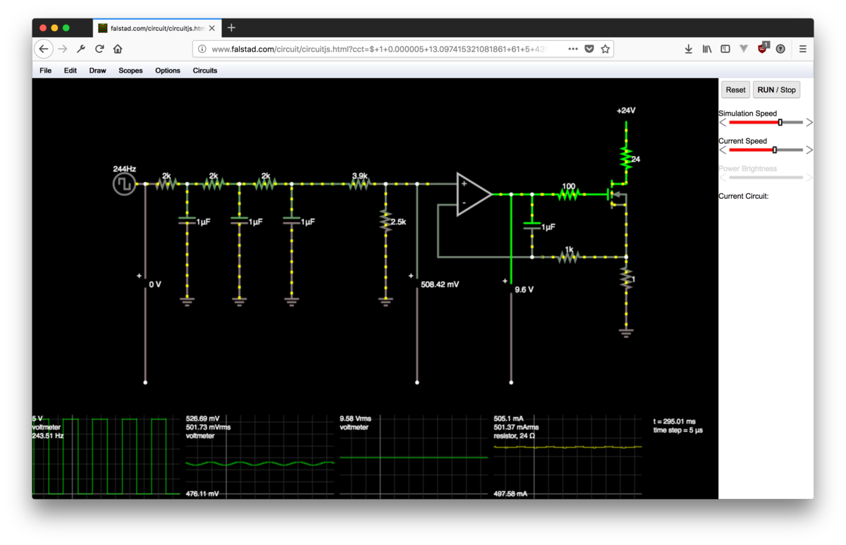
A 3-stage RC low-pass filter is between the µC and the opamp’s input. I choose 3x (2kΩ and 1µF) in series, which gives quite a smooth DC @244Hz with 50% duty cycle. Another µF is added at the opamp’s output. The simulation (link below) shows that our resulting output current has a remaining ripple of only roughly ±4mA.
Voltage divider
As our target current range is 0-1A, we need a 1/5 voltage divider to convert our µC’s 5V (@ 100% PWM duty cycle) signal to a 1V opamp input, which should yield a 1A constant output. Our filter already adds 6kΩ of series resistance. Adding another 3.9k in series and 2.49k to ground gives us the following divider ratio:
(6k+3.9k+2.49k) / 2.49k ≈ 4.976
That’s close enough to our 1/5 target ratio. We don’t need to know the actual current so accurately, as long as we make sure the maximum possible current is in the range of what our LEDs can handle.
VCCS
As described earlier, a voltage controlled current sink (VCCS) will be used to drive the LEDs through an op-amp/mosfet combination, where the op-amp is configured in a way that the current on the output matches the voltage on the input.
This works by feeding the voltage drop over a shunt back to the inverting input of an opamp. The shunt is in the ground path of our load (the LEDs). By knowing the resistor value of the shunt, we know the voltage at the inverting input for a given current (eg. 1V if the current is 1A and the shunt has 1Ω). This creates a closed loop, in which the opamp tries to keep the current through the shunt constant, provided that we ensure a constant voltage level at its non-inverting input. That voltage level is what controls the output current, which should explain the name voltage controlled current sink.
In our example (1V, 1A, 1Ω), that would mean, if we apply 0.5V to the non-inverting input of the opamp, we get 0.5A through the shunt. And the current at the shunt equals the current at each component in series with it, according to Ohm’s Law.
Simulation
An online simulator helps me validate the circuit before bulding it (click image to open live simulation):
Parts Choice
Shunt
The current sense resistor value has to be choosen as small a possible in order to minimize power dissipation. In our case – provided that we don’t want to add another amplifier circuit – we also want it to be sufficiently high so the resulting voltage drop is stable compared to the provided control voltage. I am not sure how to characterize this, only thing i know is that the external resistance should be as small as possible, compared to the input impedance of the opamp.
A differential of 1V for the entire control range seems not too generous (as mentioned, no idea how to calculate this in advance), so i’ll aim for that. This means the shunt will be 1Ω. At 1A, the resistor will turn 1W of power turned into heat – which is still acceptible, considering the total power output of the LEDs. Therefore, if we go with a resistor rated at 2W, we should be safe.
The tolerance should be small, but it doesn’t really affect the stability of the system, if it isn’t 99% accurate. It just creates a small offset between control voltage and output current. No big deal, so even a part rated at 5% tolerance should do.
Opamp
I will check if one of the opamps from the standard inventory will do the job.
MOSFET
The 50V / 16A N-channel MOSFET form the standard inventory is actually fairly oversized, but it’s also cheap – so why bother ordering any specialized components?
Design
Board
Here’s the design of the driver board hosted at upverter:
VCCS Module
It features two instances of the VCCS circuit which i designed as a separate module:
Here’s an export from 12.06.2018 hosted on the fabacademy servers:
Driver Board
- IllumiNative-Driver-Board-BOM.csv
- IllumiNative-Driver-Board-gerber+drill.zip
- IllumiNative-Driver-Board-netlist.csv
- IllumiNative-Driver-Board.openjson.upv
- IllumiNative-Driver-Board.pdf