Week 6
Electronics design
This week the theme was "Electronics design".
The objectives of this assignment were:
The objectives of this assignment were:
- Redraw the echo hello-world board, and add (at least) a button and Led with resistor.
- Check the design rules and test it.
- Extra credit: simulate its operation.
- Extra credit: render it.
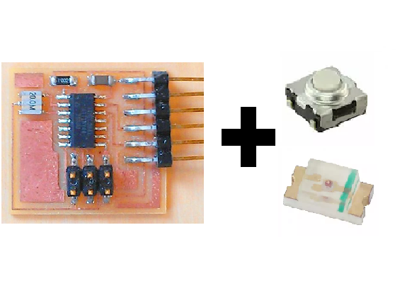
In the previous figure, we see the Hello-Word PCB provided by FabAcademy.
My work scheme was:
- Gather information about Hello-World board
- Extract the list of materials
- Select and use the software for the redesign
- Milling the board
- Weld the components on the plate
- Verify welding
- Use the programming board made in week 04 to program the Hello-world board
- Test with the Led and the button
The Hello-World board
The main component of the Hello-world board is the ATtiny44 microcontroller, this microcontroller has 14 pins, in the following picture we can see the pin-out.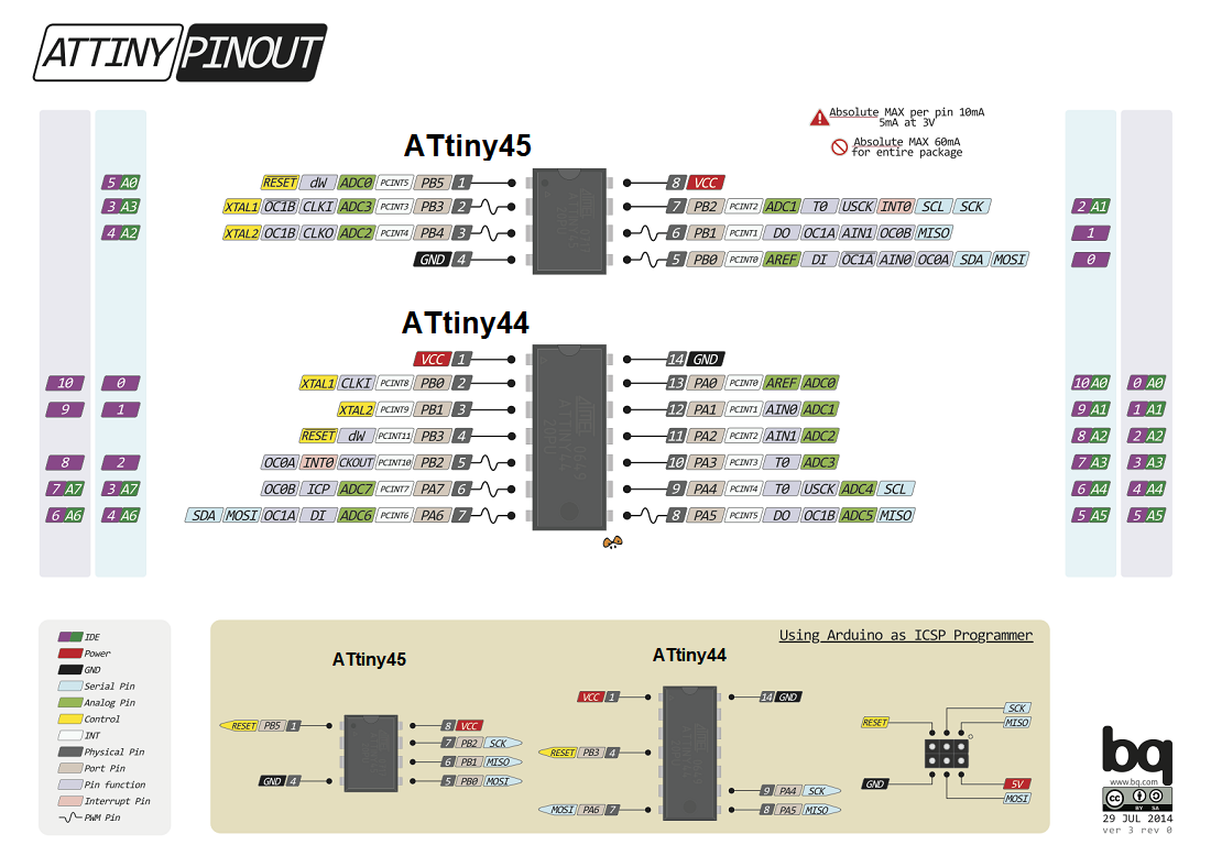
Image source: https://www.14core.com/datasheets-pin-outs/
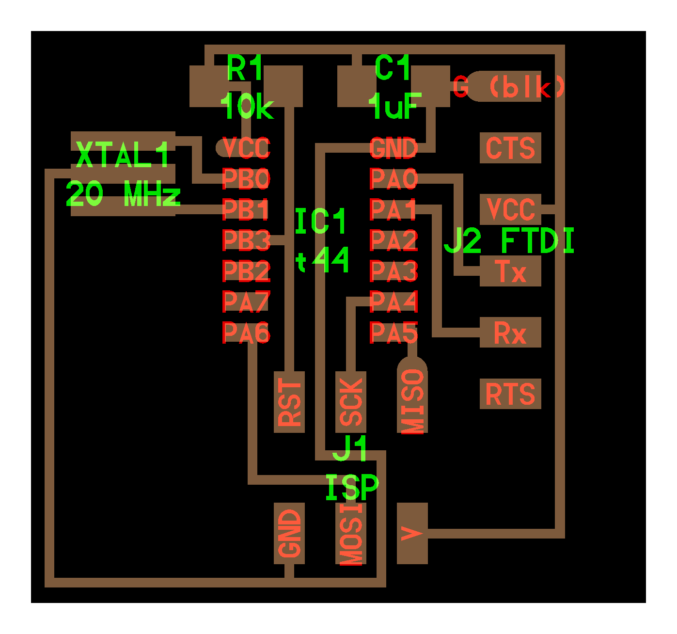
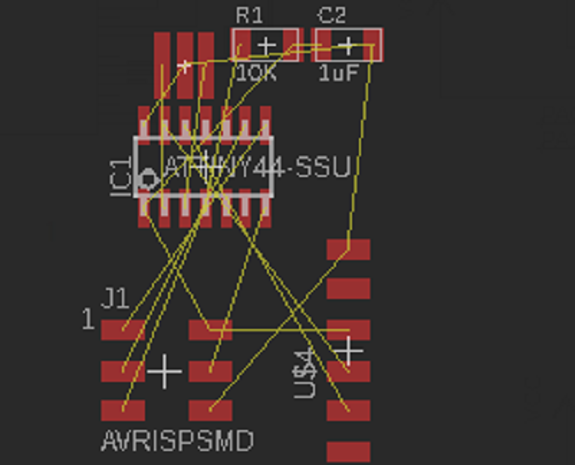
The bill of materials it was extracted from the schematic diagram shown on the right
I compared the schematic diagram with the pin-out, this helped me to identify the pins and their functions in the board and also to choose which pins to connect the led, the resistance and the button..
Bill of materials:
I compared the schematic diagram with the pin-out, this helped me to identify the pins and their functions in the board and also to choose which pins to connect the led, the resistance and the button..
Bill of materials:
- 1 ATtiny44 microcontroller (IC1)
Data sheet - 1 Resonator 20MHz (XTAL1)
- 1 Resistor SMD 10KΩ (R1)
- 1 Capacitor SMD 1µF (C1)
- 1 6-pin header (J1)
- 1 FTDI SMD header (FTDI)
For the design of the new pcb I used the Eagle of Autodesk software (the latest version)
Previously I had used Livewire and PCBWizard, but once I tried Eagle I liked how easy and intuitive its use.
Previously I had used Livewire and PCBWizard, but once I tried Eagle I liked how easy and intuitive its use.
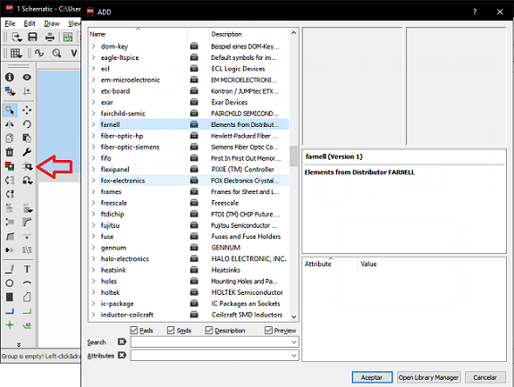
The first thing I did was load the Fab library provided by FabAcademy, you can download it from this link.
fab.lbr
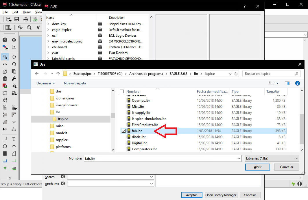
Recommendation
Once the library is downloaded, we move it to the Eagle lbr \ ltspice folder, using the file browser with administrator rights, if necessary.
Recommendation
Once the library is downloaded, we move it to the Eagle lbr \ ltspice folder, using the file browser with administrator rights, if necessary.
I created a new scheme, and started adding the components of the Fablab library, by clicking on the "Open library manager" button.
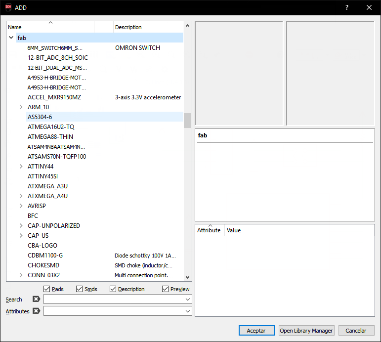
Next, I added all the components: ATtiny44, the resonator, connector ICSP, etc.
With the "Net" icon I connected each component guiding me through the labels.
You can also use labels to simplify the view. Labels with the same name are connected internally.
You can also use labels to simplify the view. Labels with the same name are connected internally.
After connecting all the components, with the button "generate / change to the board" switch to the route design mode to define the location of each component and trace the connection routes.
After many attempts, I finally fit the components and the routes without crossing them, but I still had to add the button and the led.
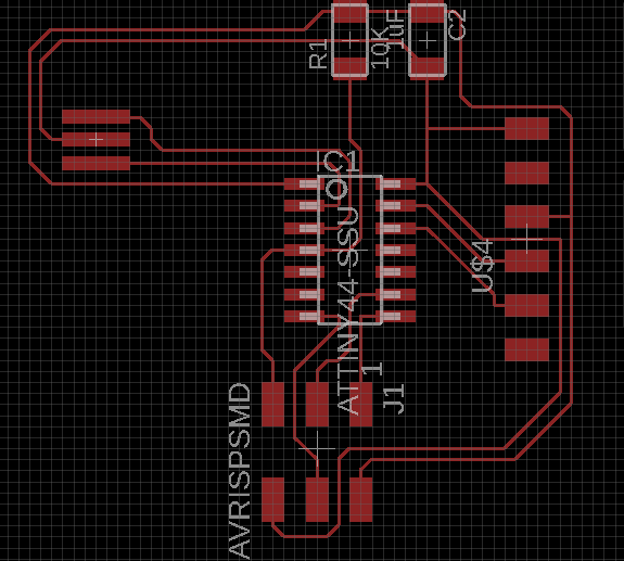
Initially I wanted to put a button and 2 leds, but the distribution of the routes was complicated by
the position of the components, so I decided to change to a single led with its resistance.
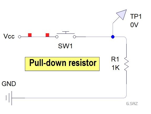
I started with the button, I chose pin 5 of the controller because it was unused.
I wanted that when the button is pressed, the tension on pin 5 is high and while not press the button the tension is low, for this it should be connected to ground, but with a resistance, so there would not be a short circuit when the circuit is closed. This resistance is called pull-down resistance.
I wanted that when the button is pressed, the tension on pin 5 is high and while not press the button the tension is low, for this it should be connected to ground, but with a resistance, so there would not be a short circuit when the circuit is closed. This resistance is called pull-down resistance.
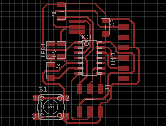
Then it was the turn of the Led and the resistance. I connected pin 6 to a 499Ω resistor, the led anode to the resistor and its cathode to ground.
As you can see in the following figure.
As you can see in the following figure.

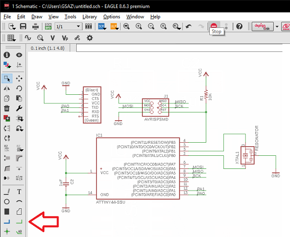
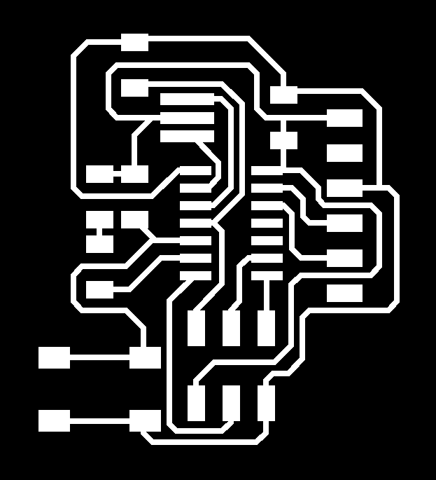
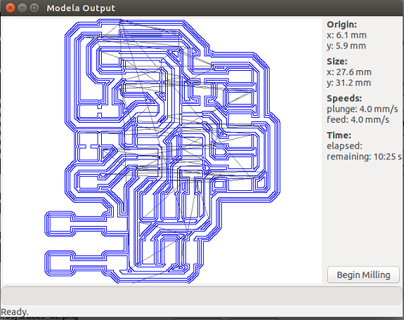
This is the final distribution of the components and routes of the
new "Hello-world" board.
This is the schematic file Schematic.sch
This is the schematic file Schematic.sch
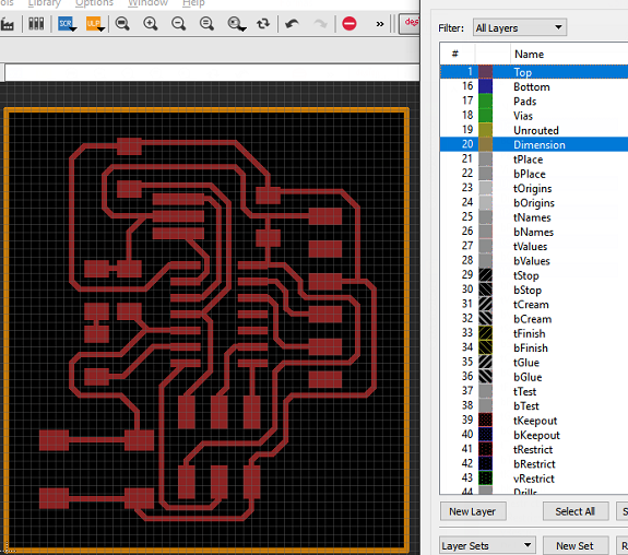
To prepare the necessary files for the milling machine I entered the menu "View / Layer settings ..."
From there the layers are shown or hidden
From there the layers are shown or hidden
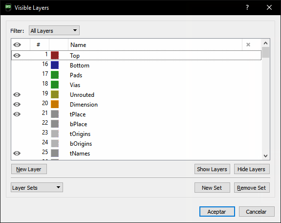
To make the traces file I only left the "Top" layer visible, and for the internal file, I left the "Dimension" layer visible
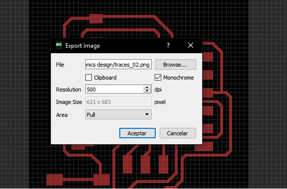
then I exported the image as a 500 dpi monochromatic PNG file

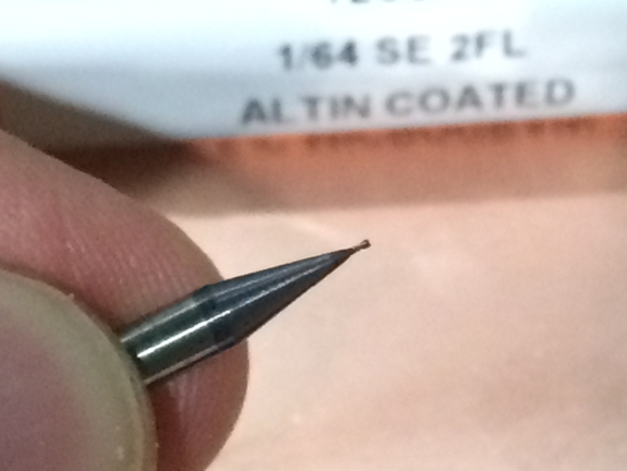
For the milling of the board I used the milling cutter 1/64"
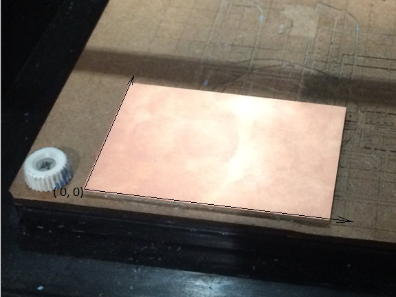
I placed my 2"x3" board in the lower left corner of the Roland milling machine.
The lower left corner of the router corresponds to the 0,0 coordinates of the software. Following the steps of my assesment "Electronics production" I started to mill the PCB.
The lower left corner of the router corresponds to the 0,0 coordinates of the software. Following the steps of my assesment "Electronics production" I started to mill the PCB.
I loaded the file "traces.png" into the software and proceeded to create the paths on the PCB.
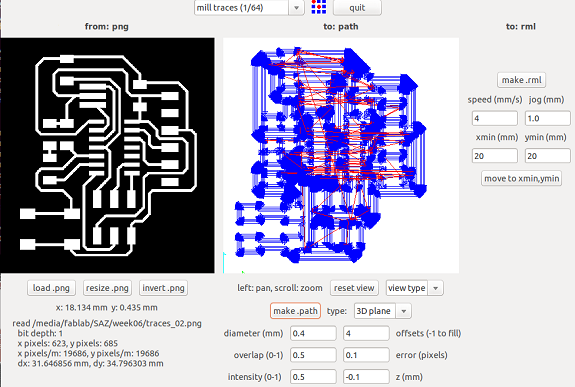
Then, I calibrated the height and proceeded to mill.
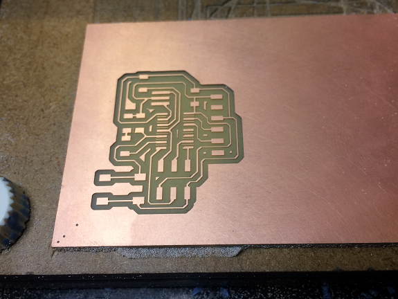
Once the milling was finished, I cleaned and checked the PCB, and everything was fine.
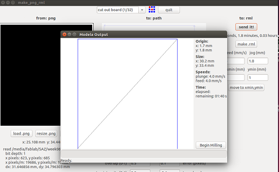
Then, without removing the PCB, I loaded the file for the PCB cut: "Interior.png".
I proceeded in the same way, calibrated the height and started milling.
I proceeded in the same way, calibrated the height and started milling.
Bad news
Cutting milling started at the calibration point!
I forgot to move the milling drill to the same position after calibrating.
Solution
Milling the PCB again and pay attention to the positions of the calibration and the start of milling.
Cutting milling started at the calibration point!
I forgot to move the milling drill to the same position after calibrating.
Solution
Milling the PCB again and pay attention to the positions of the calibration and the start of milling.
Here we see the milling of the paths of the new PCB, there was space, so I used the same material.
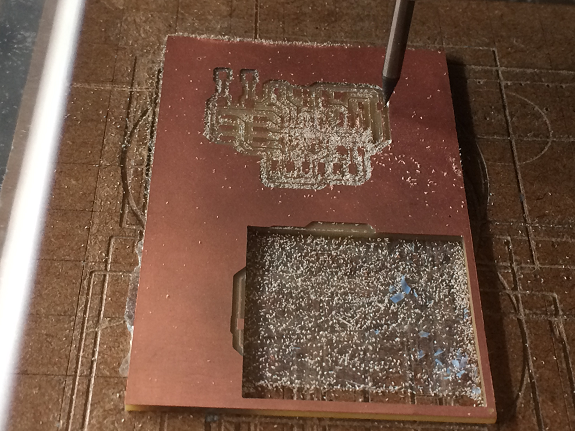
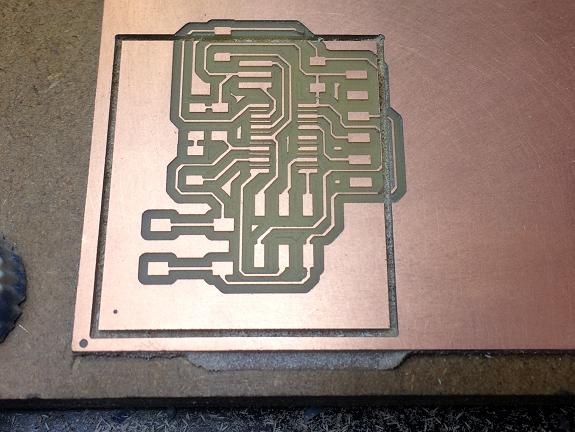
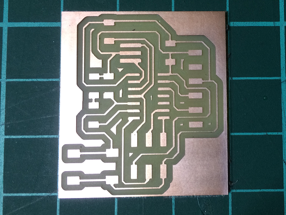
Here we can see the finished PCB and ready to weld the components.
Weld the components on the plate
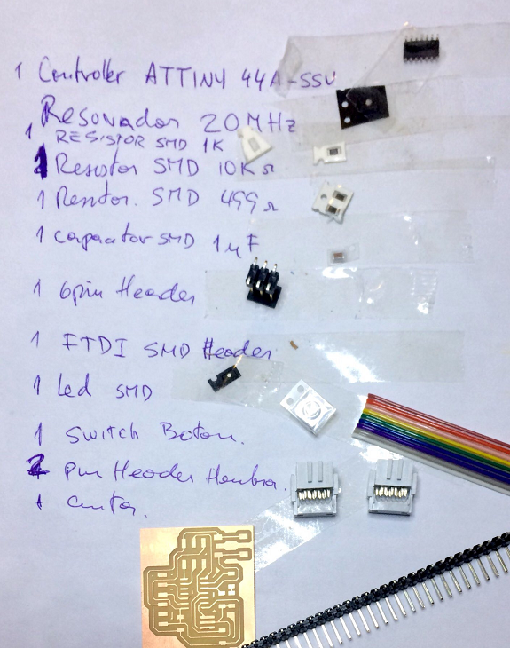
I extracted the list of materials from the schematic.
- 1 ATtiny44 microcontroller (IC1)
Data sheet - 1 Resonator 20MHz (XTAL1)
- 1 Resistor SMD 1KΩ (R5)
- 1 Resistor SMD 10KΩ (R1)
- 1 Resistor SMD 499Ω (R2)
- 1 Capacitor SMD 1µF (C1)
- 1 6-pin header (J1)
- 1 FTDI SMD header (FTDI)
- 1 Led SMD (Led1)
- 1 Switch boton SMD (S1)
- 2 Pin header female
- Ribbon Dupont Cable
Cautions

- The tip of the welder reaches a temperature between 200°C (392°F) and 400°C (752°F), be very careful, it can cause serious burns.
- Do not touch or hold any component with your fingers during welding, the heat of the welder moves quickly through the components being welded.
Do not forget
Pin # 1 has a small circular mark, place it in the same position as in the diagram.
Pin # 1 has a small circular mark, place it in the same position as in the diagram.
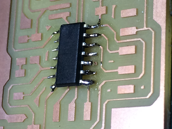
I started by welding the controller, it was the second controller that I soldered.
To prevent it from moving from its place I put adhesive tape on one end of the controller, then put a solder point on one of the pins, removed the tape and soldered the pin on the other end. Finally, I soldered the rest of the pins.
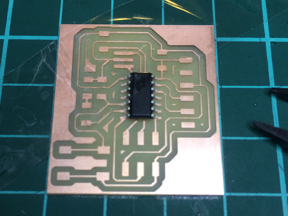
I have soldered all the pins of the controller. I will try to improve the welding.
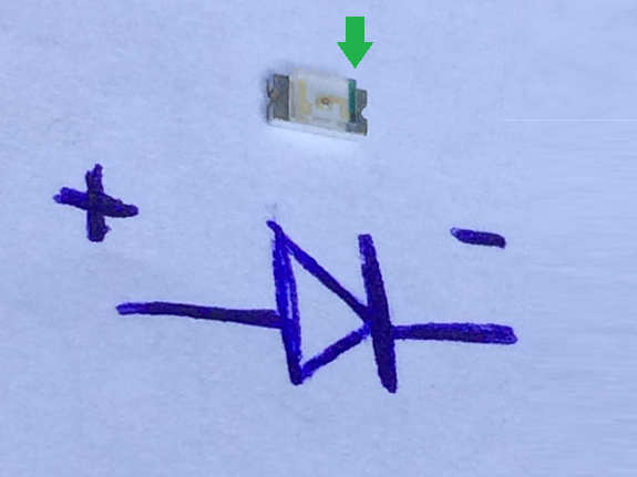
To weld the Led, care must be taken, as it has polarity. It has a green color mark on one end, that side is the Cathode (-) and must be connected to the GND.
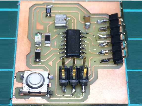
I have soldered all the components of the PCB.
I have checked all the welding points.
I have checked all the welding points.
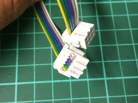
The next step was to prepare the programming cable. I cut only 6 wires from a piece of Dupont tape. And I assembled the female connectors.
Correct way to assemble the cable
Here you must be careful with the connectors. The same Dupont ribbon wire (in this case yellow) must be connected to the connector side that has the manufacturer's mark.
Here you must be careful with the connectors. The same Dupont ribbon wire (in this case yellow) must be connected to the connector side that has the manufacturer's mark.
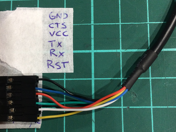
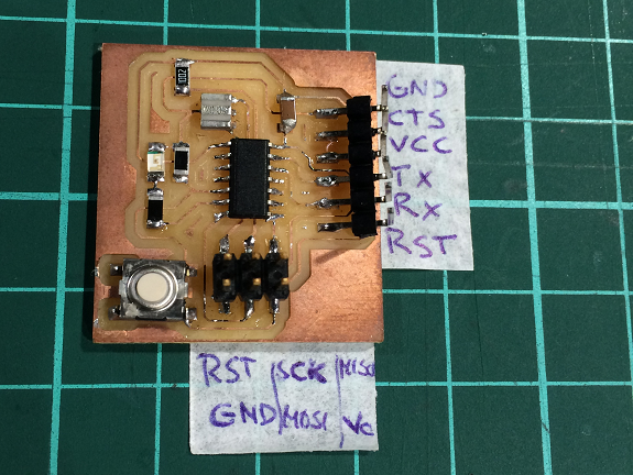
Once the ISP cable was finished and all the welding points of the PCB checked, I labeled the order of connection of the FTDI and ISP cables.
This is the FTDI cable that I will use in the next "Embedded Programming" assignment.
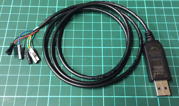
Each wire of the FTDI cable has a color that identifies it, this is the order to connect them.