Week 10
Input Devices
Assignment
Group
• measure the analog levels and digital signals in an input device.
Individual• measure something: add a sensor to a microcontroller board that you have designed and read it.
Group Assignment
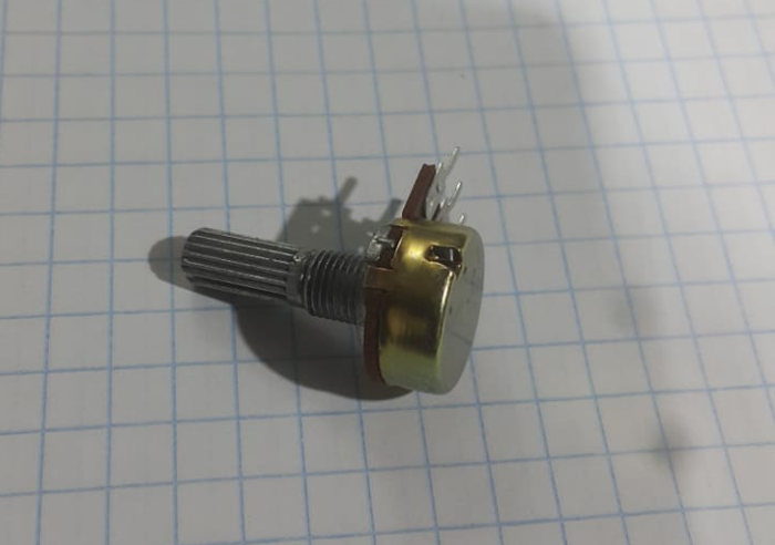
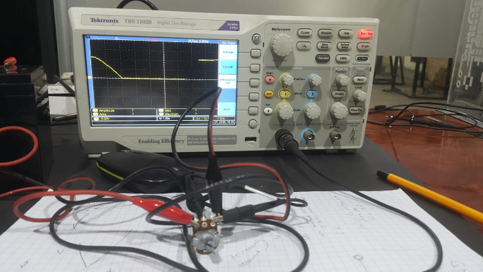
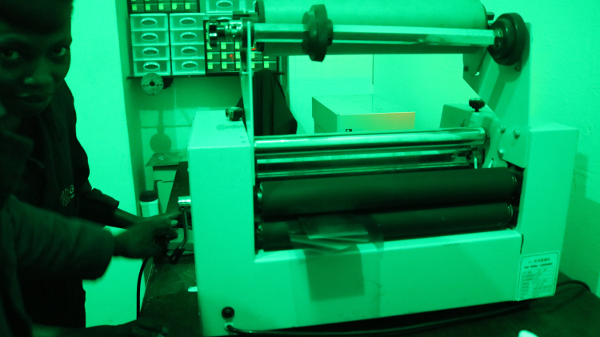
Linear potentiometer has three terminal resistor which adjusts the voltage through the rotating nobe.Am using oscilloscope as shown, I connected the vcc of the potentiometer to a power battery and GND to the ground of the potentiometer. Then connected the oscilloscope probe pins to vcc and the pin out of the potentiometer as shown.
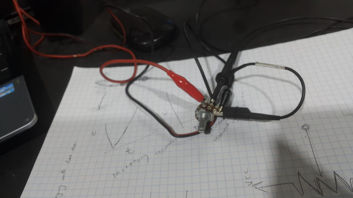
using the rotating nobe in the potentiometer to test the varying leves of voltage as shown.
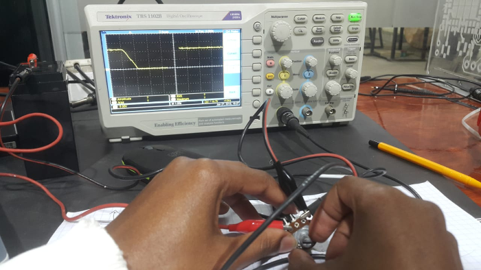
While increasing the resistance of the rotating probe to the ground the voltage was rising proportionally as shown.
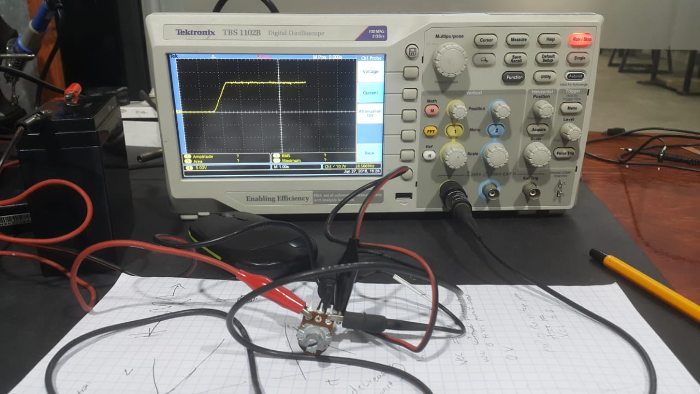
While decresing the resistance of the rotating probe to the grounD the voltage was falling proportionally as shown.
Ultrasonic Sensor
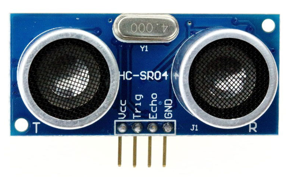
For this assignment i decide to use an ultrasonic sensor.
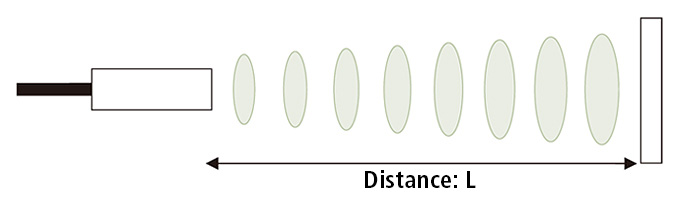
An Ultrasonic sensor is a device that can measure the distance to an object by using sound waves. It measures distance by sending out a sound wave at a specific frequency and listening for that sound wave to bounce back. By recording the elapsed time between the sound wave being generated and the sound wave bouncing back, it is possible to calculate the distance between the sonar sensor and the object.
This is the sensor am using.
Design process
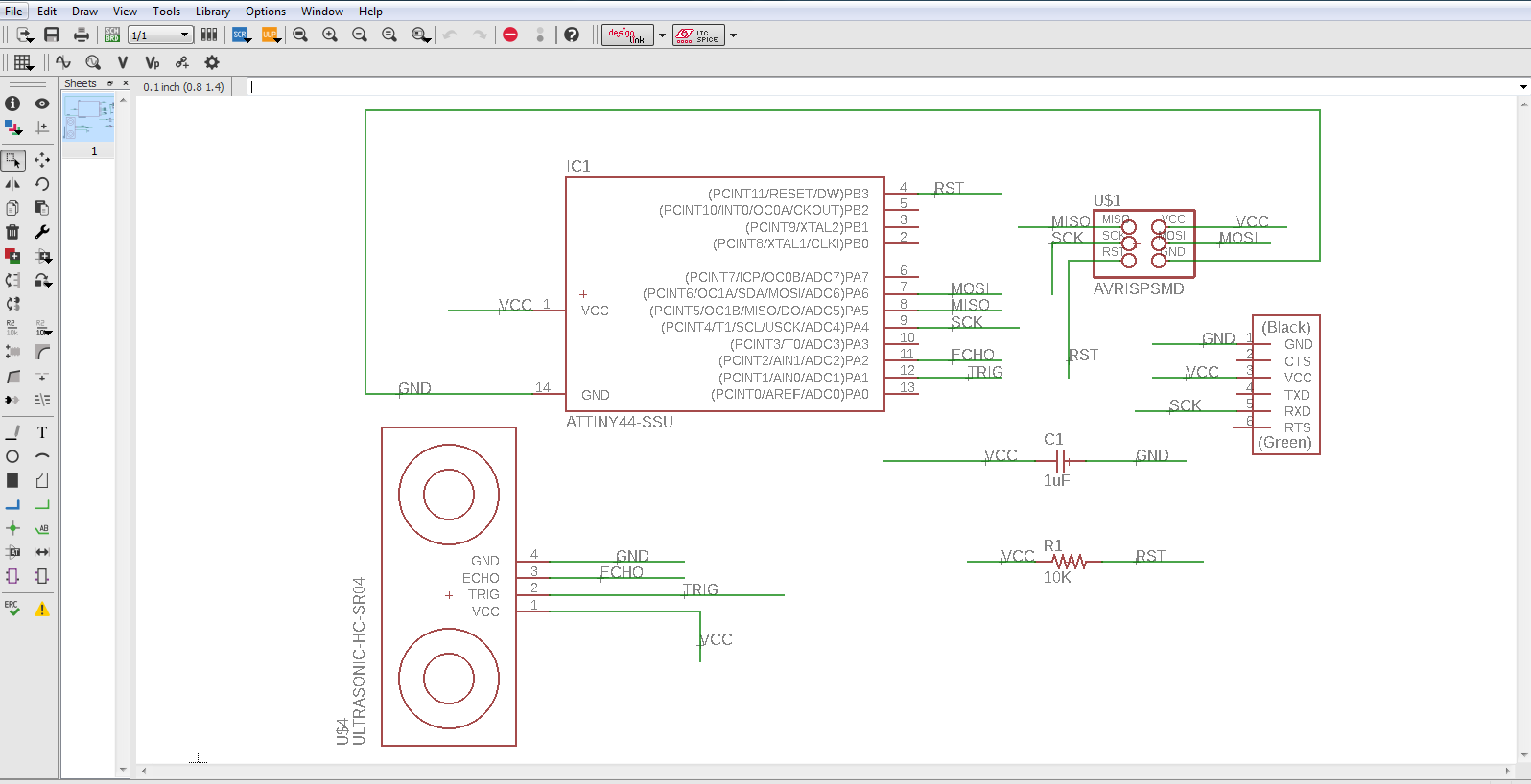
The below board i used to reference and help me design the board as per the input device that am using on this case.
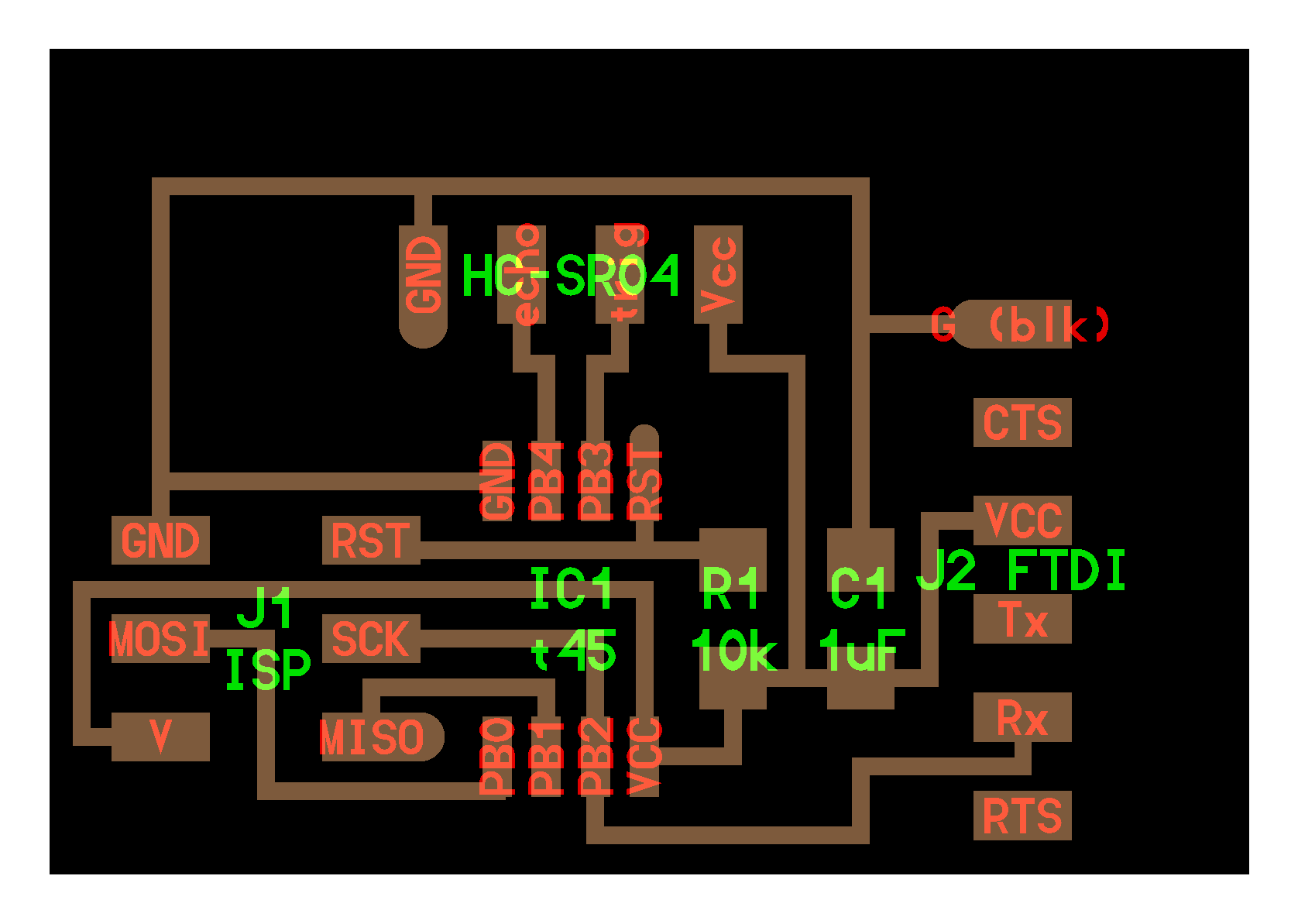
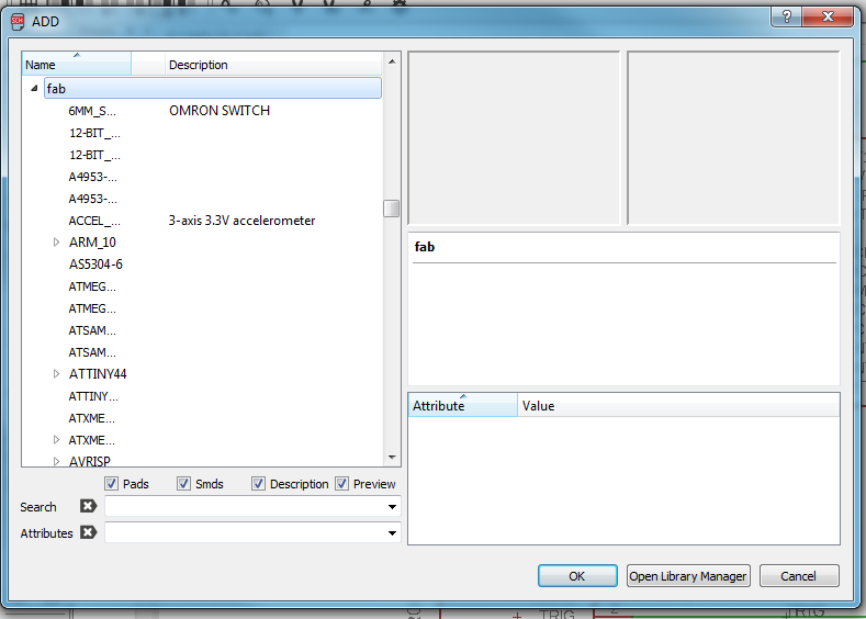
Using the fab library that is where i got most of the components and very helpfull because it has alot of components. I used the add component button as shown... After adding all the componets, you just pick the component you need and drag it to the schematic workspace and it get displayed. I used the connector to connect the components together making reference to the board above.
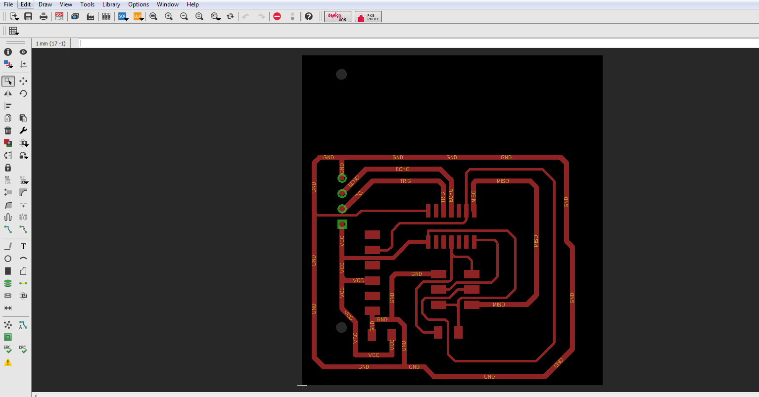
Making the screen board I used this button to generete the board. It prompts you if you want to create a board from your schematic, after selecting yes the below diagram is waht you see.Then from there i used the moving tool to drag the components inside the black screen.I arranged them based on the connections between the components themselves.
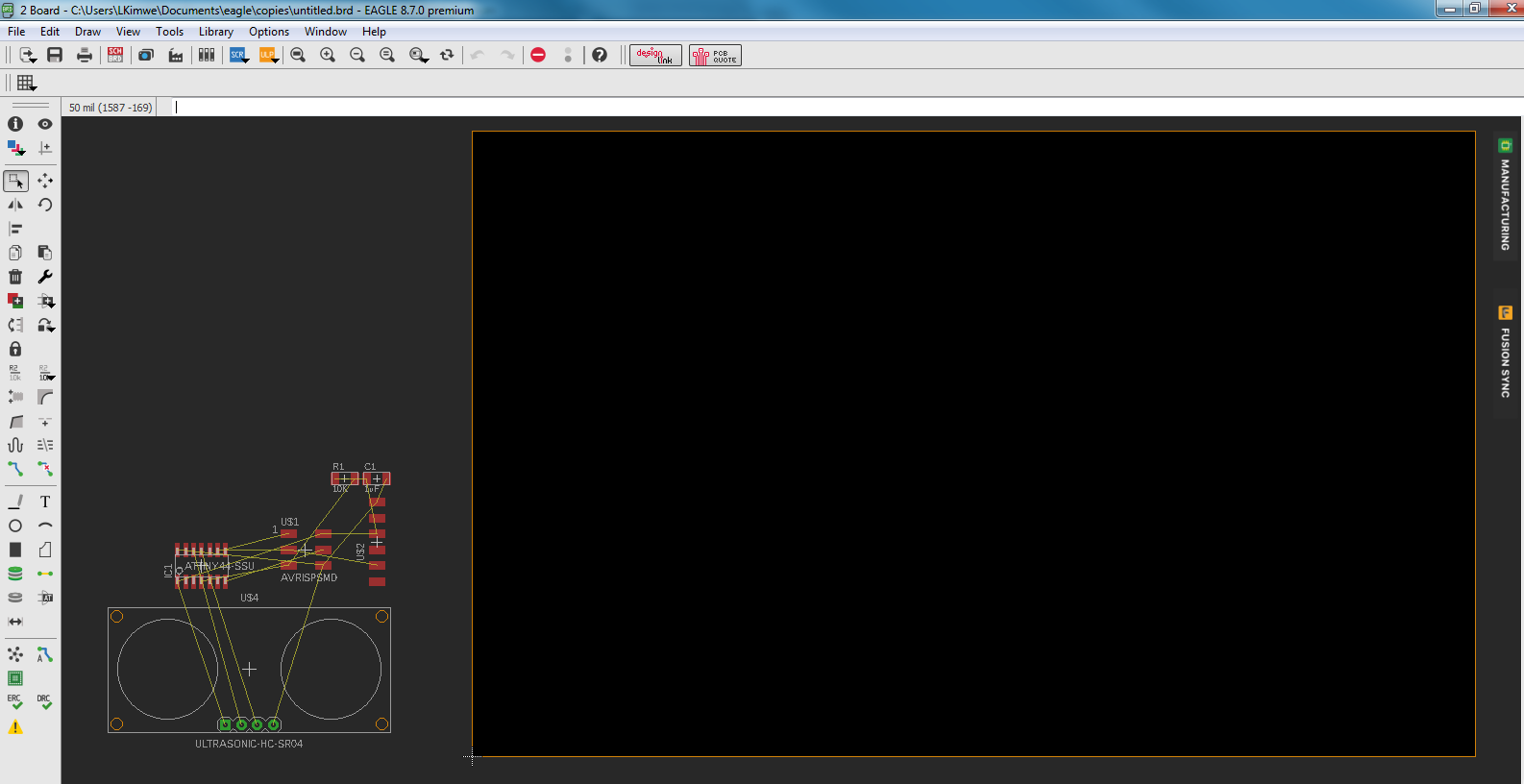
Since i did not want to design my board on the whole screen i used the dimension tool to give dimension to only the space i wanted to work with.
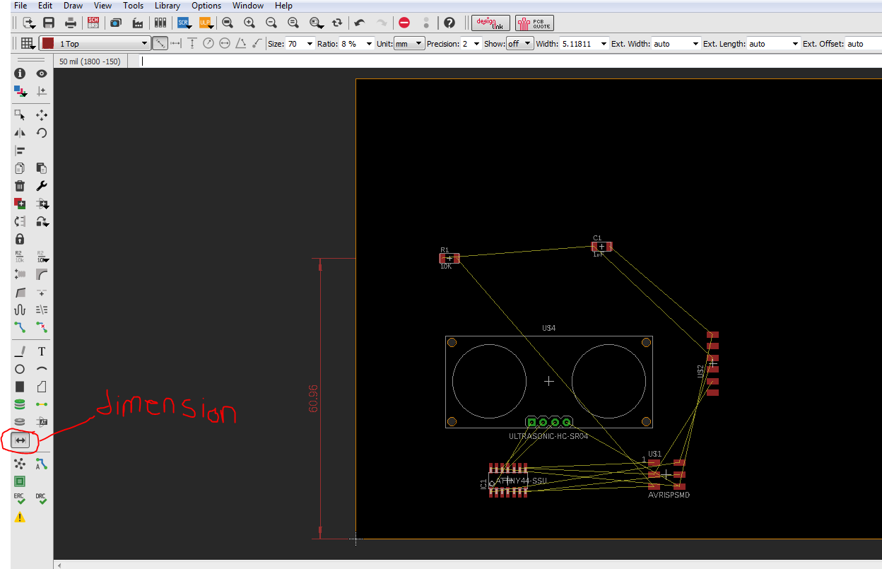
I used the connector tool to make the connections and other tools to complete the design.
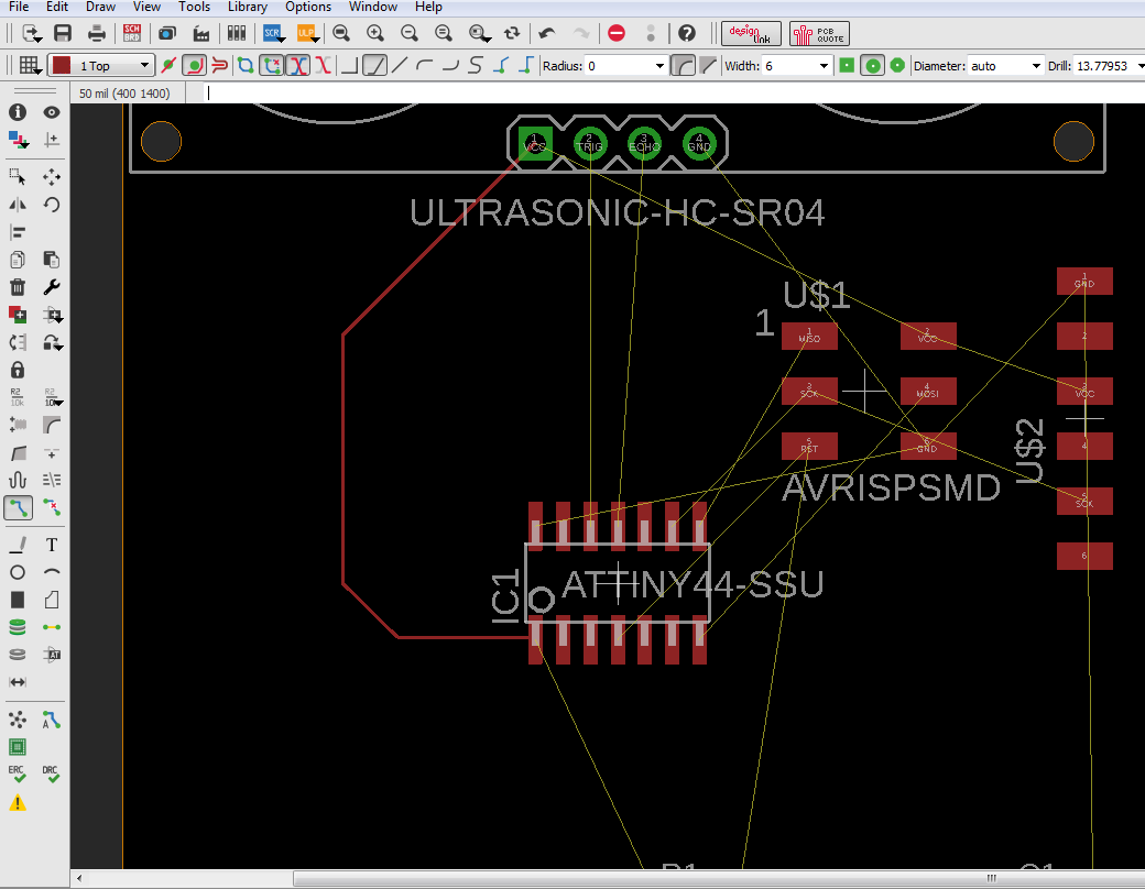
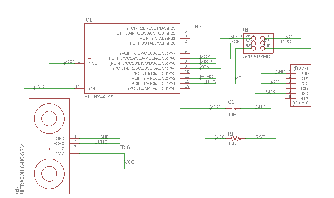
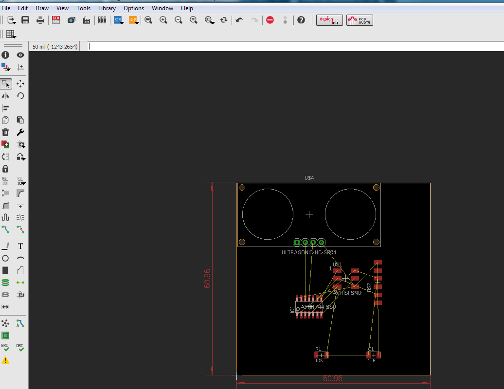
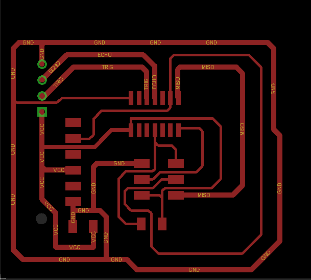
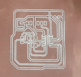
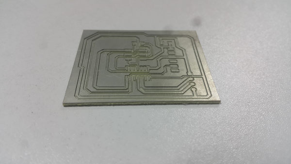
This is the final diagram.
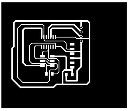
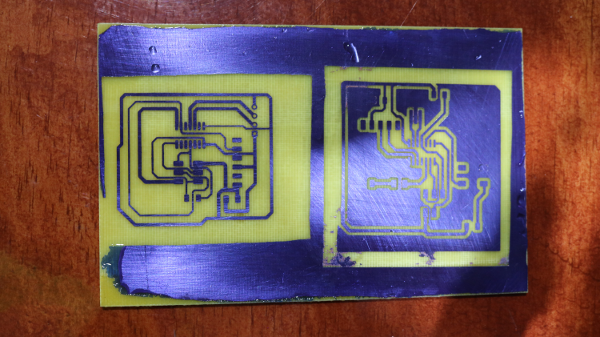
The print version of the diagram.
Components
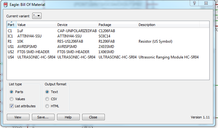
These are the components that i used for the design. I used the ulp tool to view all the components and their value in th eeagle software. It shows you all the components hence its very effective when you want to know exactly what values your components without having to remember all of them.
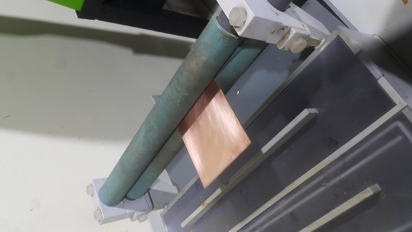
The fabrication Process
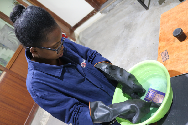
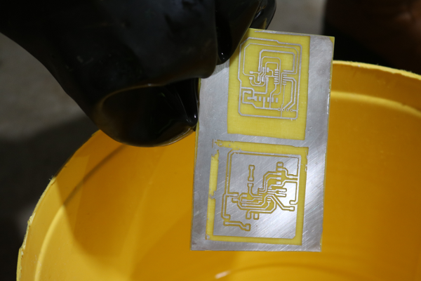
This board I made using the etching process and i did it together with the hello board in th electronic design.So am gonna copy the same process here.
The first step was cleaning the etching board with a scouring pad and washing agent.
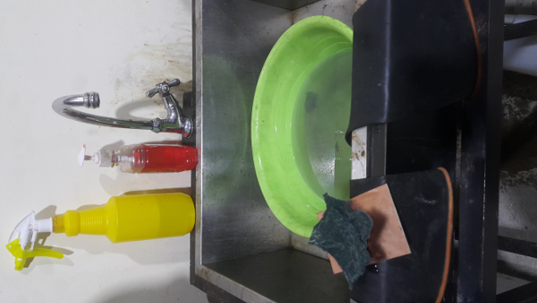
After cleaning it I dried it by pressing it through a drying sponge .
Then i Used a drier to completely remove the excess water.
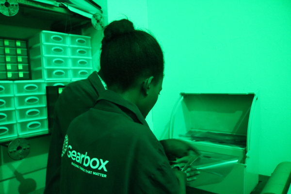
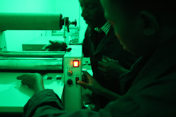
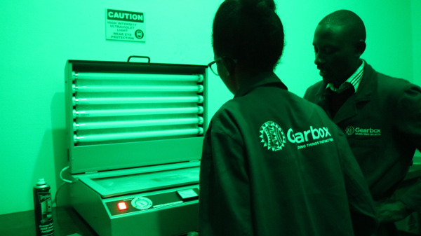
The next stage followed was a photoresist process where i laminated the board with a photoresist film. Worked with one of our lab engineers here at Gearbox.
I was told that the film has three layers so we used the maskingtape to remove one of the film. The photoresist is in themiddle so we had to remove the top film and the remaining sticky part i put it on the board.
Then i used the lamination machine to press the photoresist material to the board. We used 75 degrees celcius to laminate the board. The machine has two sides so at first I pressde it then laminated.
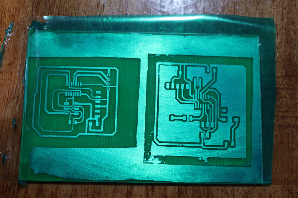
Then I put the board design that i had printed on the board
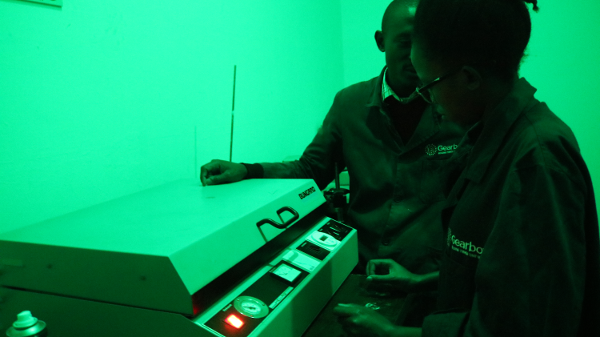
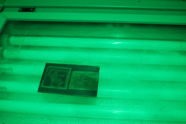
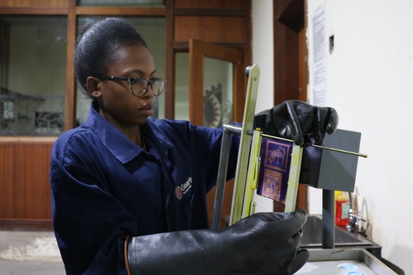
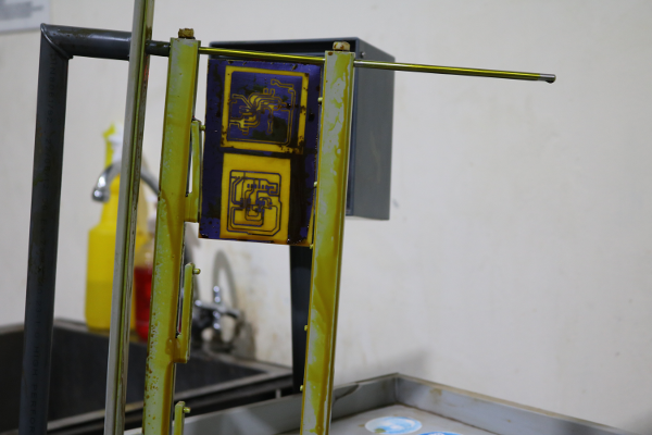
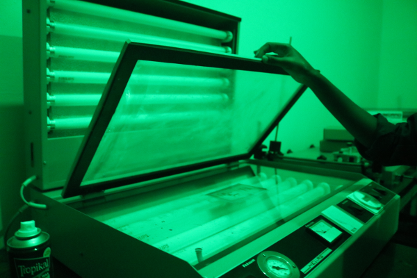
The next step was exposure using the bungard exposure unit. The unit has an inner layer called the vacuum that sucks the air out of the board once you place the board. Then press the ventilator button basicalluy want it does is to remove th eair around the board.
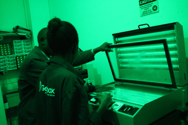
Then exposed the board into the UV light rays for 6 seconds.
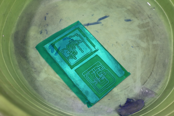
Developing stage
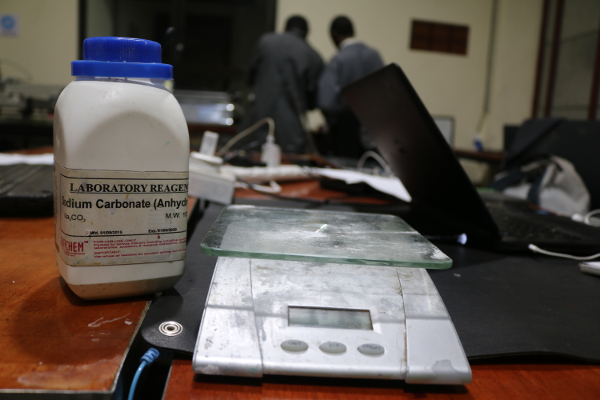
Fistly i removed onother layer of the film. Then did a mixture of 100ml of water to 2g of sodium carbonate. In this case i used 500ml of water to 5g of sodium carbonate.Then dipped it in th esolution for sevreal minutes.
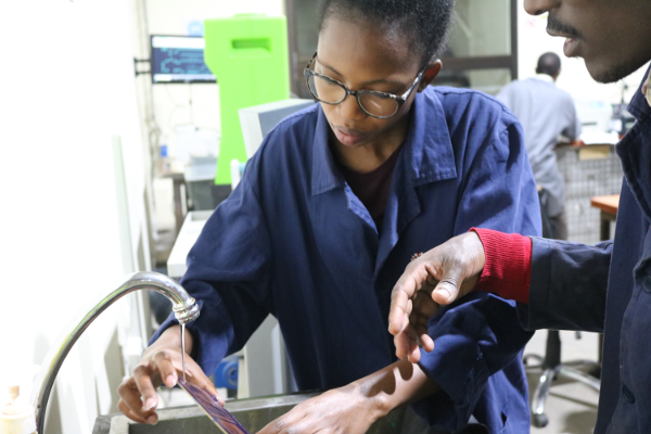
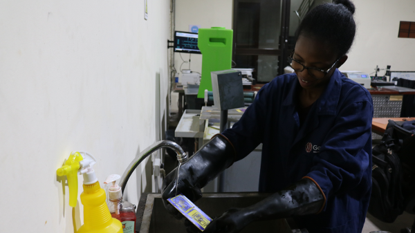
Rised it using running water then dried it.
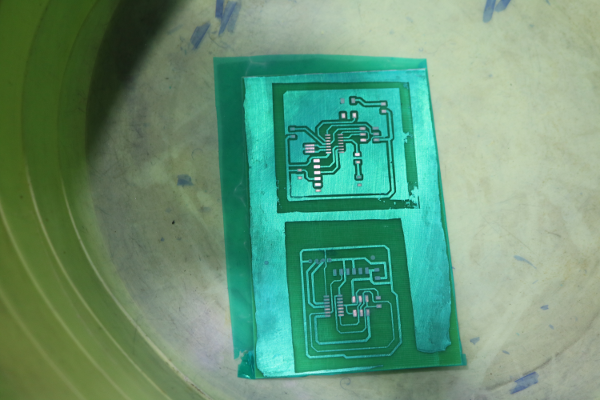
Challenge
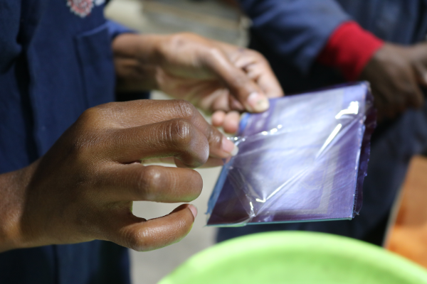
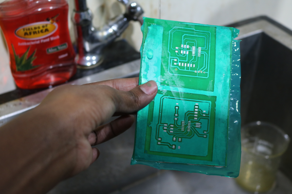
The major challenge was after dipping the board in the solution it still has some parts of the photo resist that had not come out properly so after rinsing i put it back in the bungard exposure unit and exposed it for a few seconds and the put it back to the solution and used my fingers to clean the excess material.as shown below in sequentially.
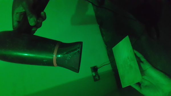
The chemical etching process
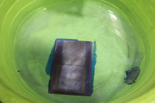
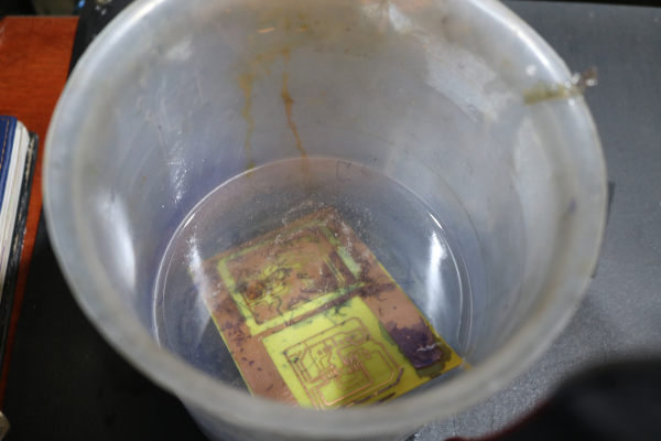
For this process I used the Bungard spalsh center machine in the lab.In splash section I used the foric chloride solution. At first had to put th eboard in place befor dipping it in the solution. The machine has a timer which you set, i set it to 5minutes.Removedi tthen rised it.
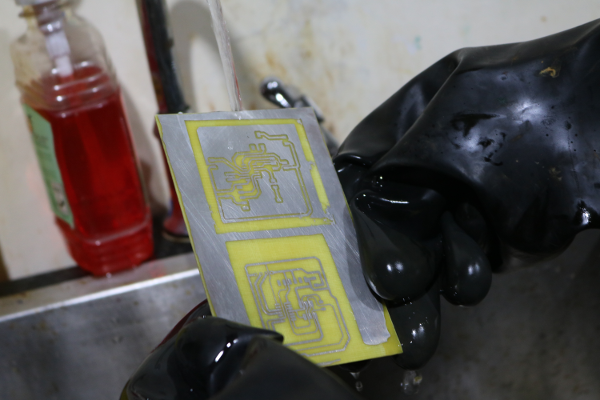
The stripping process i used sodium hydroxide with water then i dipped the board.
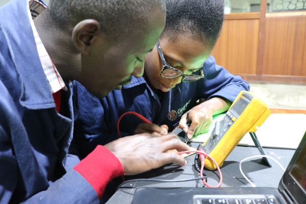
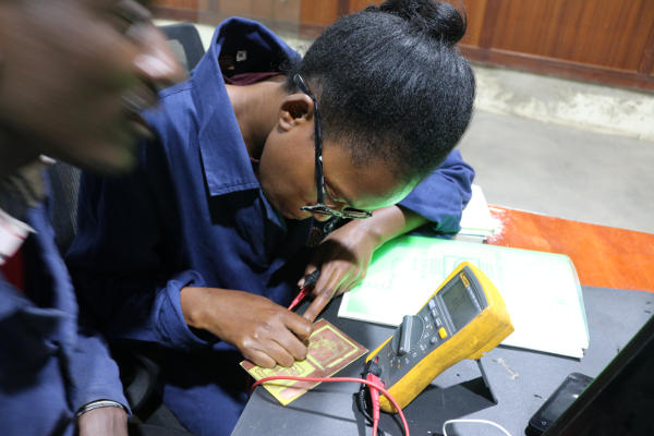
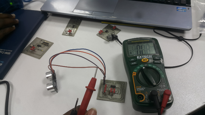
Dried the board then tested it using a multimeter the continuity of the connection between the commponents.
Challenges
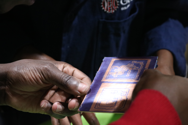
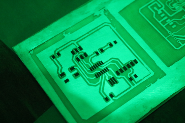
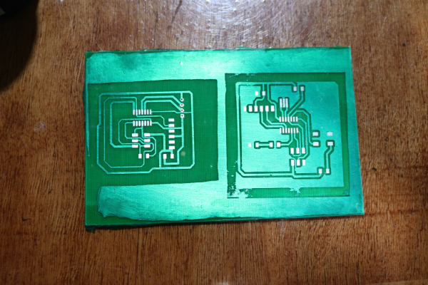
Some of the connections had connected together at some point doo i had to manually scarp of the bits of copper attaching th econnections as shown. The results
Before
After
The Tinning process
Used the tinning solution to help prevent th ecopper form oxidation. I just dipped it in the solution for a few minutes then rised it out.
Soulder Masking Process
I did almost a similar process like etching. First i covered the board with soulder mask film after removing th etop layer.Then used the lamination machine to press the film on to the board.Then printed the components from the design in eagle software. Then used the bungard exposure unit to vacuum it and passed the uv light
Once done I removed the second layer and dipped it in th emixture solution of sodium carbonate and water. Rised it then dried it.
Milling
I milled all the boards together for further information on the milling process go to week;
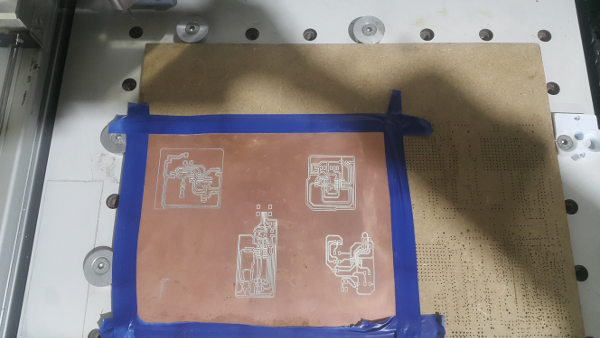
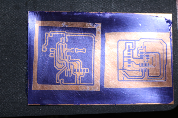
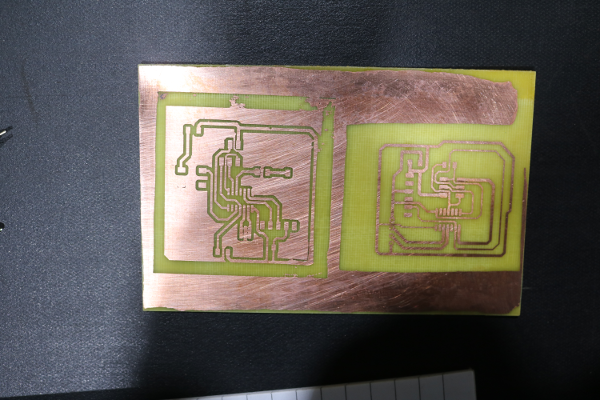
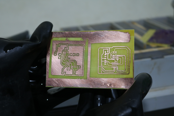
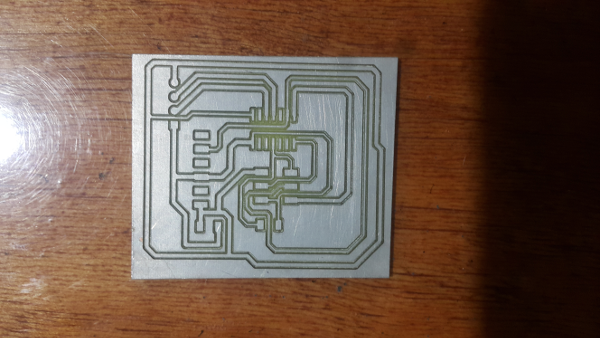
The milled board.
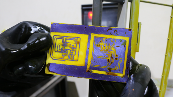
The final board after washing it and then dipped it in the tinning solution.
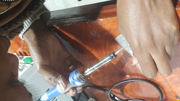
Soldering
For soldering I just used the soldering wire, flux and the soldering machine. At first I tested the continuity of the connections. The soldered and populated the board.
Programming
Using the Datasheet.
Mapping pinout of attiny44 to Neil’s code that was written for attiny45.
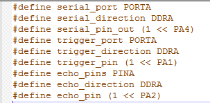
Trigpin : PA1
Echopin: PA2
Serial: PA4
Timer overflow flag is TCNT FOR attiny45 but is TCNT0 for attiny44.
The command for starting the user interface

Code modifications.Changing Header files as shown:
Changed the naming for the timer interrupt flag eg as shown below
TIFR0 |= (1 << TOV0);After modifying the code I used the make file to program the output device board.
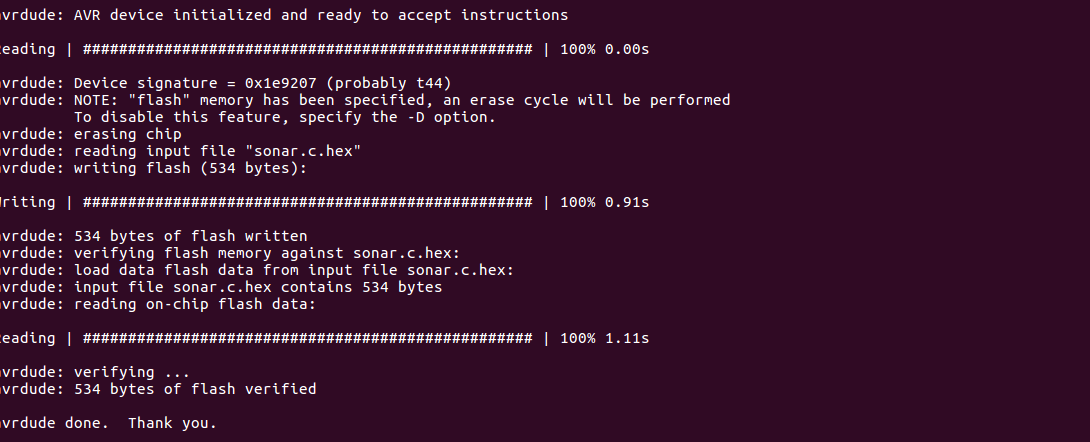
Then called the python interface as shown; Unfortunately there was no change in the interface as the ultrasonic device moved away and close to an object.
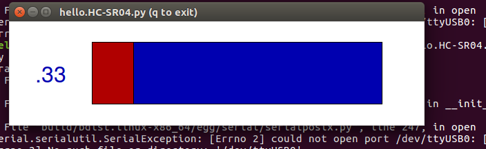
Solution
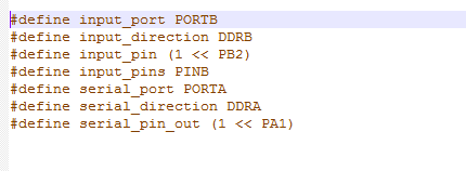
Since the ultrasonic sensor would not change the interface, I decided to work with a button which was in the hello board and modify it to suite the inout device test.
Connections
Button -> PB2
Serial (TX) -> PA1(transmit pin)
Code modifications. Code from fabacademy archives ;http://academy.cba.mit.edu/classes/input_devices/button/hello.button.45.c
Modified to fit the design of the hello,ftdi board. Used datasheet to check the pins and ports that the button eas connected and the tx pin.
Programming the board
Copied the file button.c and the makefile into one folder them changed into the directory through terminal. I then typed the command make
This gave the following feedback:
avr-gcc -mmcu=attiny44 -Wall -Os -DF_CPU=20000000 -I./ -o button.out button.c avr-objcopy -O ihex button.out button.c.hex;\ avr-size --mcu=attiny44 --format=avr button.out AVR Memory Usage ---------------- Device: attiny44 Program: 366 bytes (8.9% Full) (.text + .data + .bootloader) Data: 0 bytes (0.0% Full) (.data + .bss + .noinit)
The next command was:
sudo make -f makefile program-usbtinyWhich brought this error;
avrdude: initialization failed, rc=-1 Double check connections and try again, or use -F to override this check.
I double checked connections. Turns out there was a loose connection. I keyed in the command again and this time it was a success as indicated by the feedback below.
avr-objcopy -O ihex button.out button.c.hex;\
avr-size --mcu=attiny44 --format=avr button.out
AVR Memory Usage ---------------- Device: attiny44 Program: 366 bytes (8.9% Full) (.text + .data + .bootloader) Data: 0 bytes (0.0% Full) (.data + .bss + .noinit) avrdude -p t44 -P usb -c usbtiny -U flash:w:button.c.hex avrdude: AVR device initialized and ready to accept instructions Reading | ################################################## | 100% 0.00s avrdude: Device signature = 0x1e9207 (probably t44) avrdude: NOTE: "flash" memory has been specified, an erase cycle will be performed To disable this feature, specify the -D option. avrdude: erasing chip avrdude: reading input file "button.c.hex" avrdude: input file button.c.hex auto detected as Intel Hex avrdude: writing flash (366 bytes): Writing | ################################################## | 100% 0.60s avrdude: 366 bytes of flash written avrdude: verifying flash memory against button.c.hex: avrdude: load data flash data from input file button.c.hex: avrdude: input file button.c.hex auto detected as Intel Hex avrdude: input file button.c.hex contains 366 bytes avrdude: reading on-chip flash data: Reading | ################################################## | 100% 0.70s avrdude: verifying ... avrdude: 366 bytes of flash verified avrdude: safemode: Fuses OK (E:FF, H:DF, L:5E) avrdude done. Thank you.
To start the python terminal i used the command:
sudo python term.py /dev/ttyUSB0 9600This brought the user interface that show the feedback from the button. The letter ‘d ‘ is printed when I pressed the button and ‘u’ when I released the button as seen below.