Before two weeks we produce FabISP predesigned board we it was my first board. In this week we will design our own board also it will be my first PCB designed board.
I will explain what I did in sequential steps
Step #1
Download EAGLE software and install the necessary library
In ordar to design both schematic and PCB layout of the board I used EAGLE software. which can be downloaded from
here
if you have a AUTODESK studant account.
After installation complete I added a new schematic file. A schematic is a drawing represents connections between electronic components . Then I should add the components I need to use in my board, so I downlaoded
fab.lbr
library.
Then from Library bar, select Open library manager and broswse the location of the downloaded library then it will be automatically added to component list.
Step #2
Add desired components
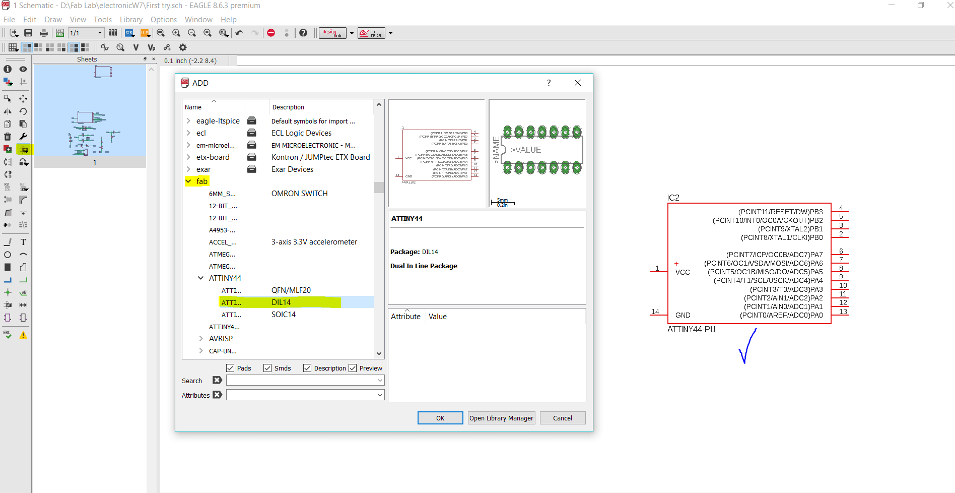
The main piece of the board is ATtiny44 IC. To add select highlighted icons in this pciture.
The same as previous step add these components:
Cystal 20MHz x 1
Capacitor 10 pF x 2
Resistor 499 Ohm x 3
Resistor 10K Ohm x 2
SMD Buttons x 2
LED x 2
AVRISP x 1 pinheader of ISP programmer
FTDI-SMD x1 pinheader of FTDI programmer
Step #3
Draw schematic diagrame Connect the circuit
Now all needed components placed on schematics file without any connection between them.
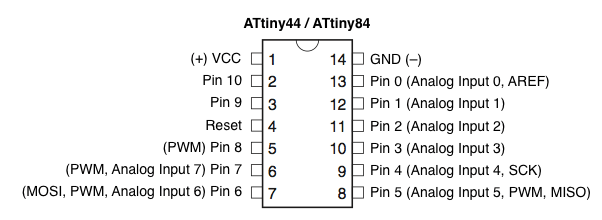
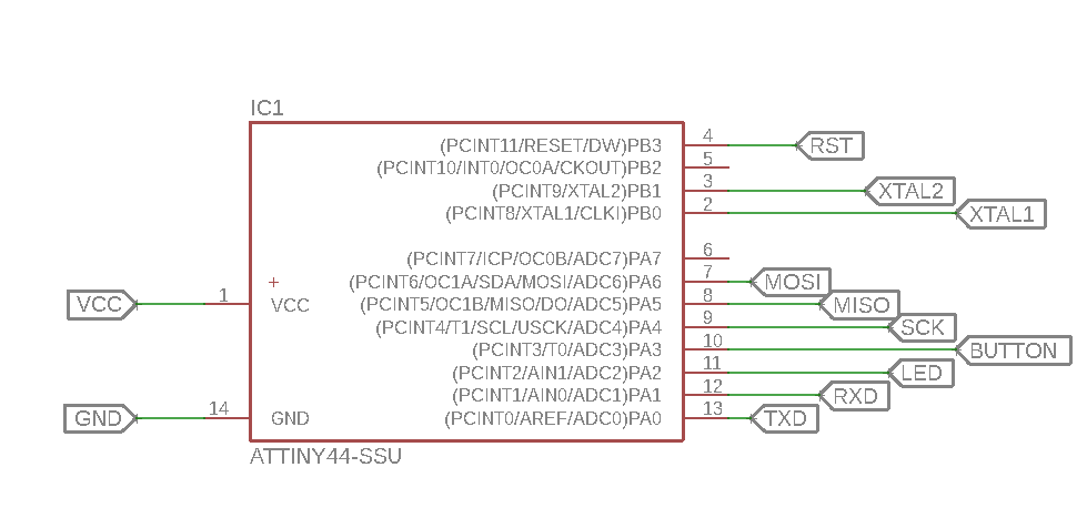
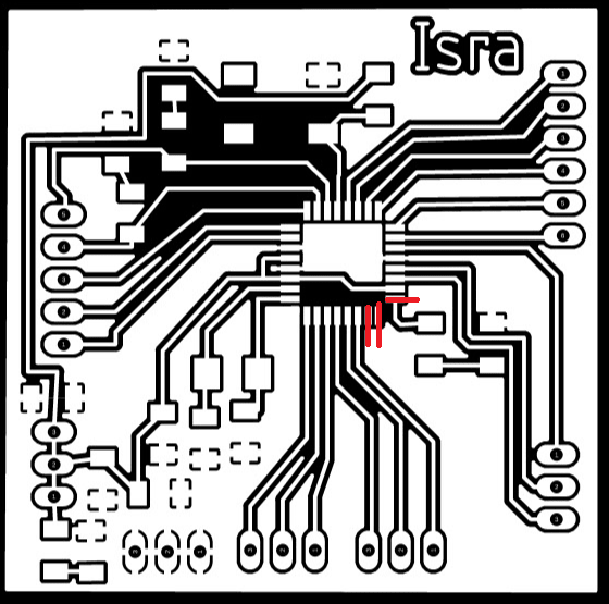
To know how to connect each pin of ATtiny44 look carefully to its Pinout shown:
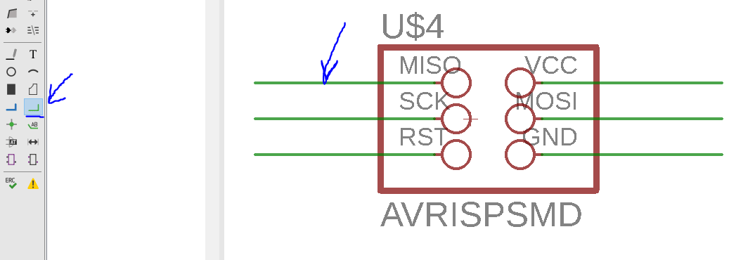
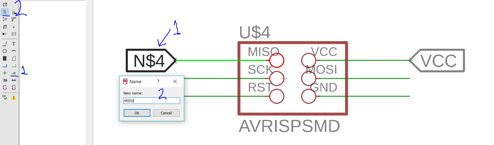
To connect components Firstly, add wires from Net icon as shown in the picture ( do this for all pins of ATtiny44, AVRISP and FTDI-SMD)
Secondly, Add a label for each wire, then rename it as shown in figure ( if two wires have the same label, it will be connected to each other this how we connect the circuit)
The full connection of each part will be illustrated separately.
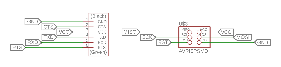
Start with ISP programmer (AVRISP) and FTDI-SMDpin headers
The connection of ATtiny44 looks like:
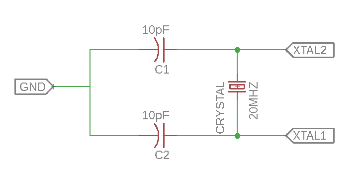
Cystal 20MHz should be connected with two capacitors to pins XTAL1 & XTAL2 of ATiny44 as shown:
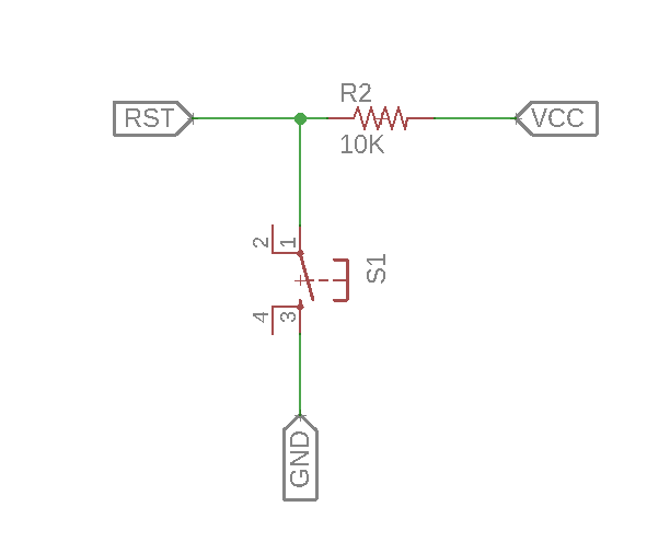
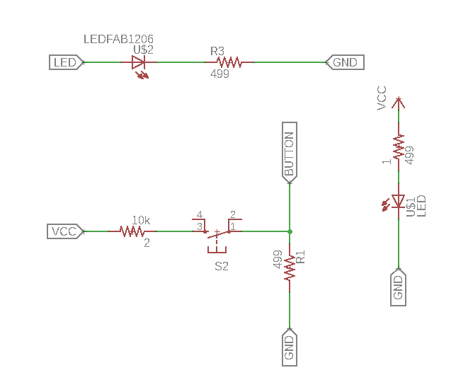
The RST label is for reset the program on micrcontroller it should be connected with VCC all the time because it is an active low pin if it connects with zero volt it will reset !. So I connected it with a button as shown:
At least the board must have all previous components. And other parts should be added!.
I decided to add two LEDs, one connected to VCC directly (when it ON that means power connected to the board( the other is connected to a microcontroller pin so it could be programmed.
I also connect a button to other pin of the microcontroller which could be programmed to do something when it is colsed ex: when I press the button the LED will blink.
All extra components shown in this figure:
Step #4
Board Layout
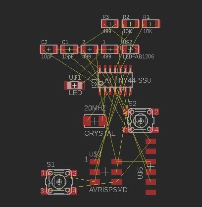
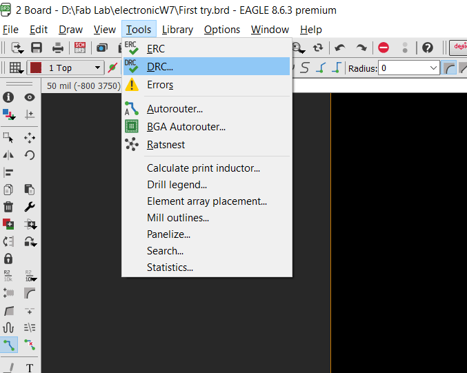
After checking all connections and make sure all is well, now arrange all components on the PCB board as it will print. This called Board layout to move to that screen, press Generate\switch to board
icon
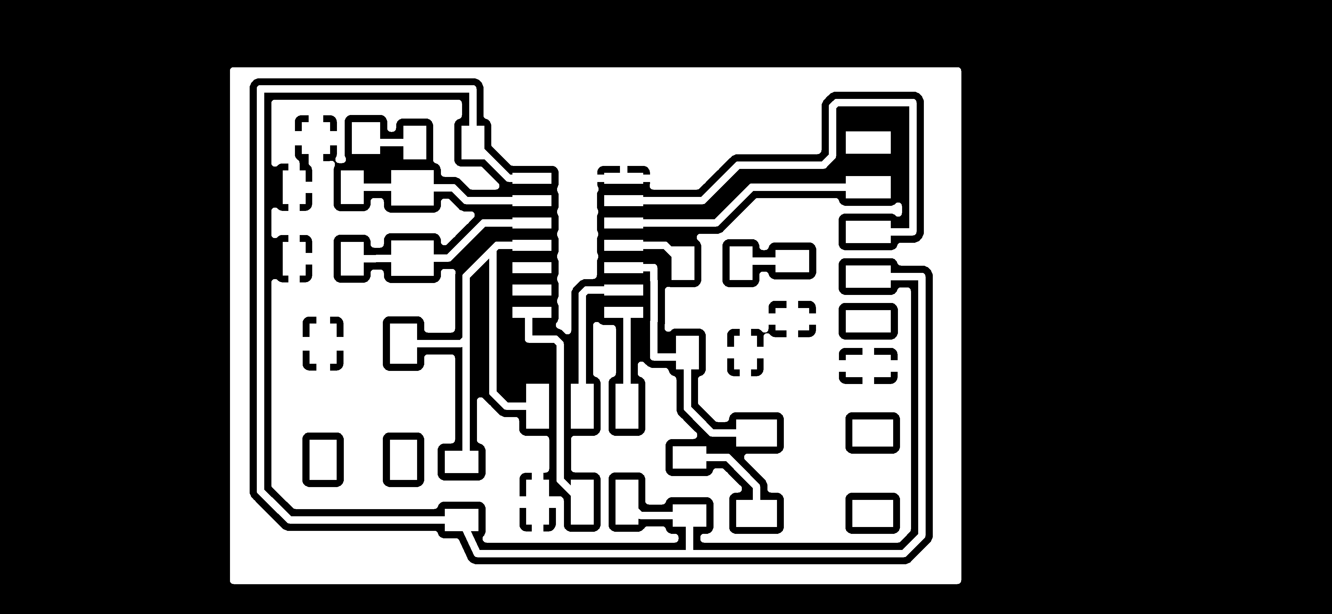
It looks like spider web!!!!!!!!!
Actually the troubles start here! I should arrange this mess and no remove all overlaps between wires. This called routing
Before begin, lets make ATtiny44 alone on one side and show how many error I have.
To do that follow these steps:
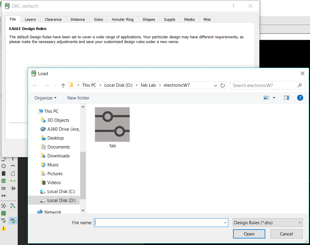
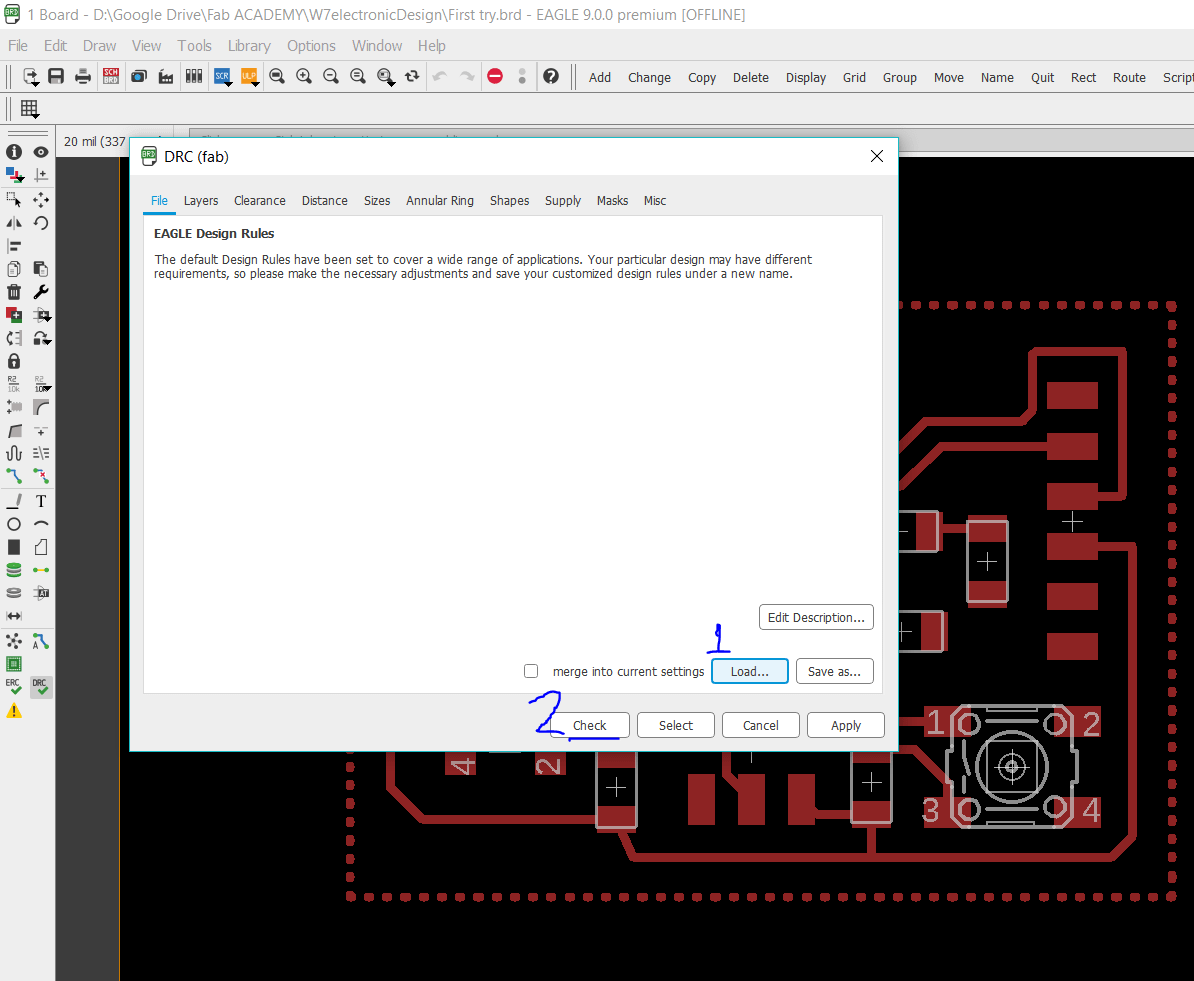
First, Download
Fab Design Rules . Then go to:
Choose previous downloaded fab design rules then press check
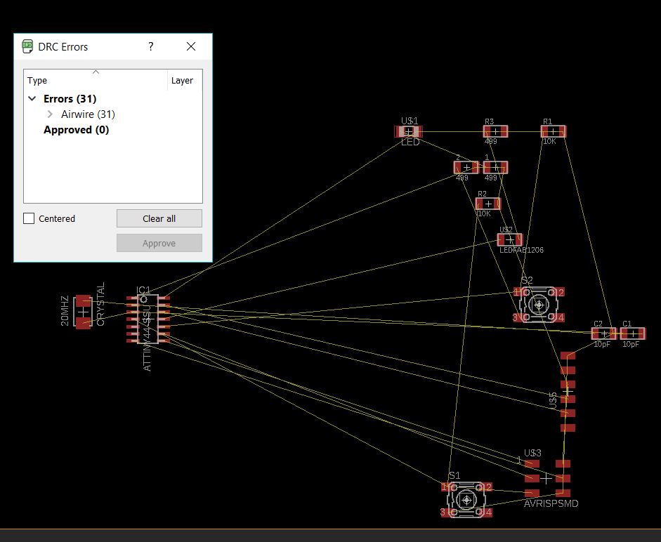
The result :
I have a lot of work to fix all of them!!
Before starting connect wires I changed the width of them to 16. This is my first time of routing at the beginning I didn't understand what's happening and what I should do to fix all of these errors.
Laetly I understand that the main concept was to put the microcontroller in the middle, then bring each component near to the pin connected to it, then connect these wires. When I press Ratsnest EAGLE will automatically update the yellow wires to connect with the nearest pin.
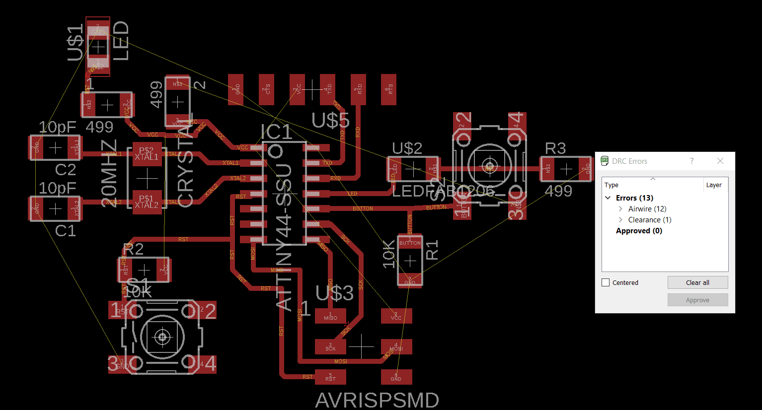
I followed this procedure but at the end, I discovered that there are unreachable pins in some places :( . So it really took too much time I repeated whole process may be four or five times (
Below some of my failed tries:
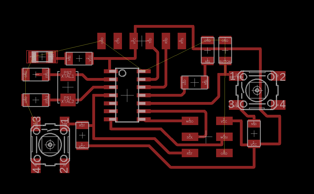
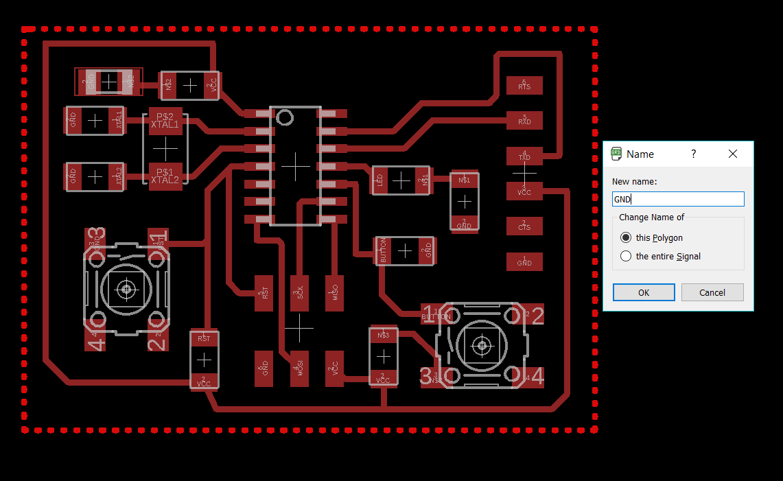
The major problem was to connect all grounds together. Finaly, our instructor showed as a very smart trick. From the left bar in EAGLE choose POLYGON and draw it around your board and renamed it to GND as shown:
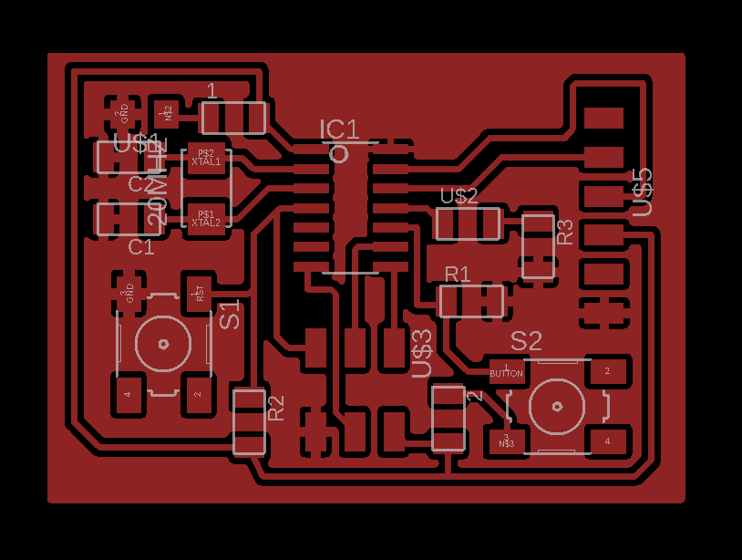
Then press Ratsnest it will make all board area as GND and separate all parts from it throw traces as shown :
Step #5
Check the Validity of the Design Using DRC Tool
To make sure there is no erorr in the design I used DRC Design Rulse Check tool, this tool check if the design meets certain rules. the main rules and brief explanation of them are listed below:
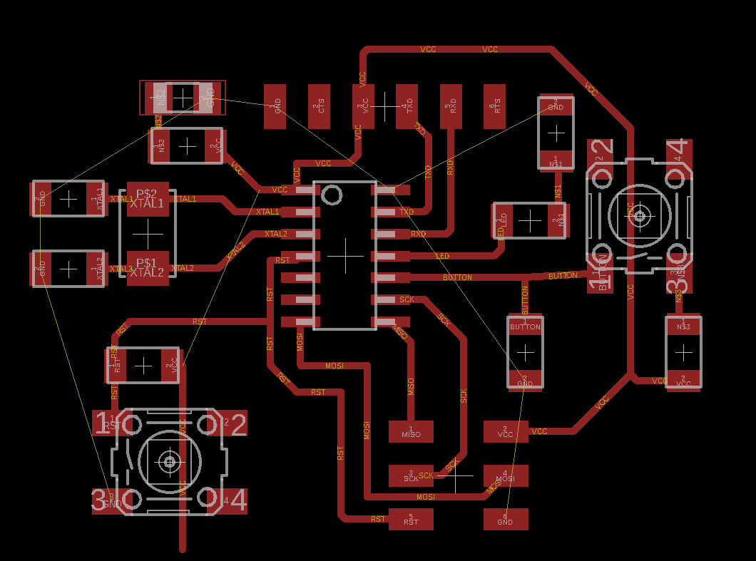
After I check it THERE IS NO ERRORS I couldn't belive that I did it :) .
Layers:
Determines which layer the board is actually using and what is the thickness of the copper and isolation of that layer.
Clearance:
Determines the minimum clearance values between different objects in single layer such as pads and wires.
Distance:
Determines the minimum distance between objects and the board dimensions also between any two drill holes.
Sizes:
Determines the minimum width of any objects also the minimum drill diameter.
Annular Ring:
Determines the width of the copper ring that should remain after drill a pad or a via.
Shapes
Determines the actual shapes for smds and pads.
Supply
Determines the dimensions of Thermal and Annulus symbols used in supply layers.
Masks
Determines the dimensions of solder stop and creak masks.
Misk
Allows the user to turn on a grid and angle check.
To make sure there is no erorrs in my design I used Fab desgin rules which I downloaded form HERE.
then I loaded the downloaded file as shown:
After I pressed checkTHERE IS NO ERRORS appear on the screen I couldn't belive that I did it :).
Step #6
Preparing files to be milled
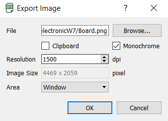
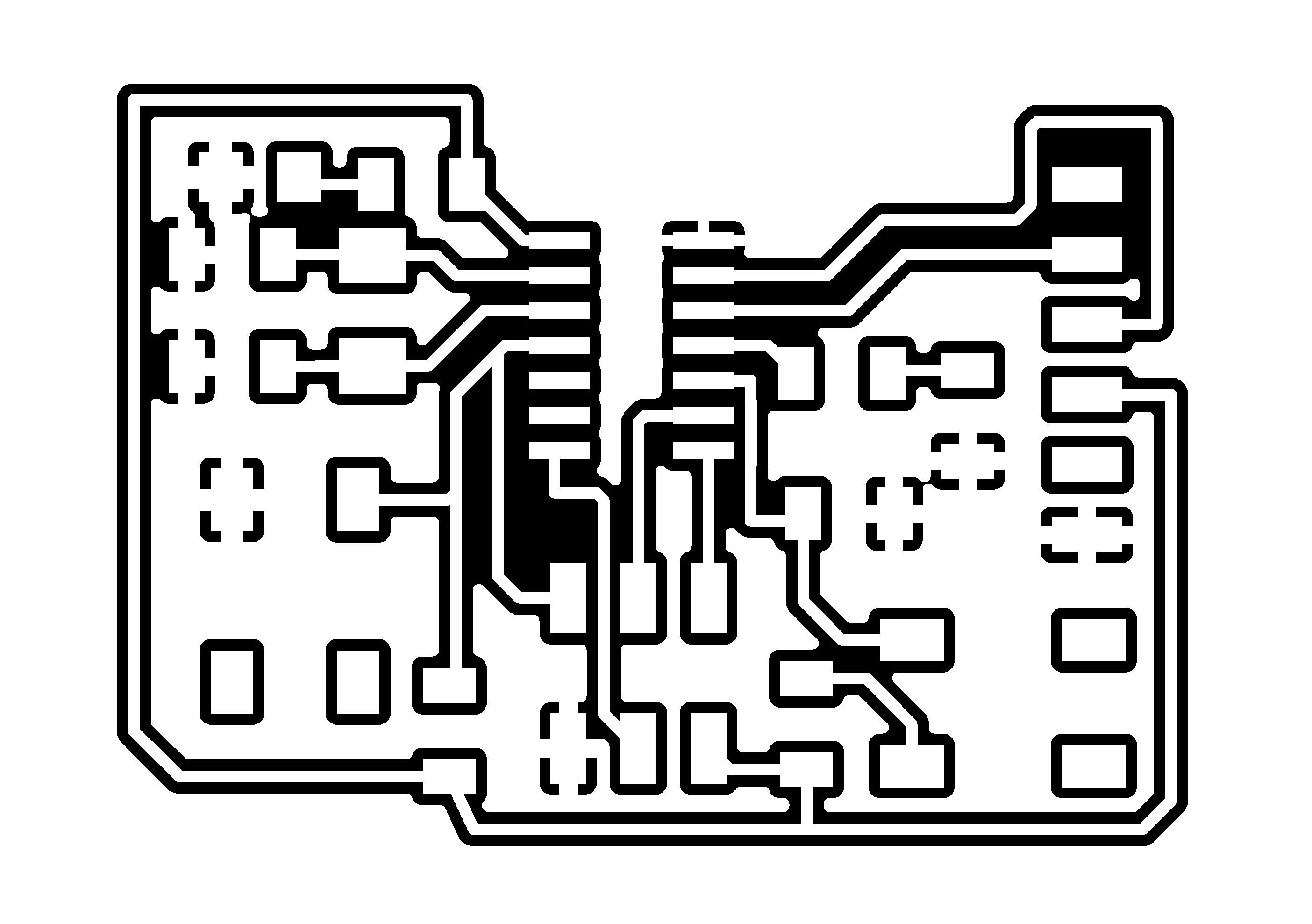
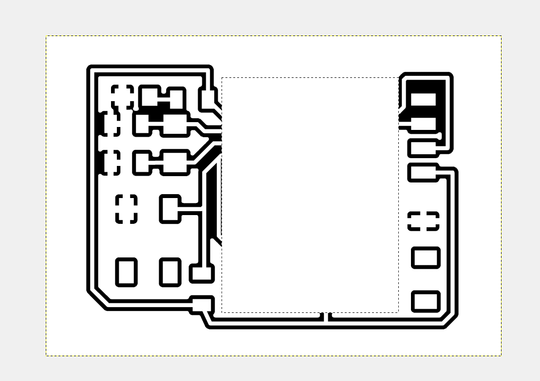
Now I will export my board layout as an image, but before that I must make Top layer the only visible laye, becuase then I need to engrave the traces only. Then from file bar, select Export - Image and choose these settings
The exported image looks like
I used
image editor free software. There I just remove the black area around my board to make the inside cut image as shown:
Then save it as .png
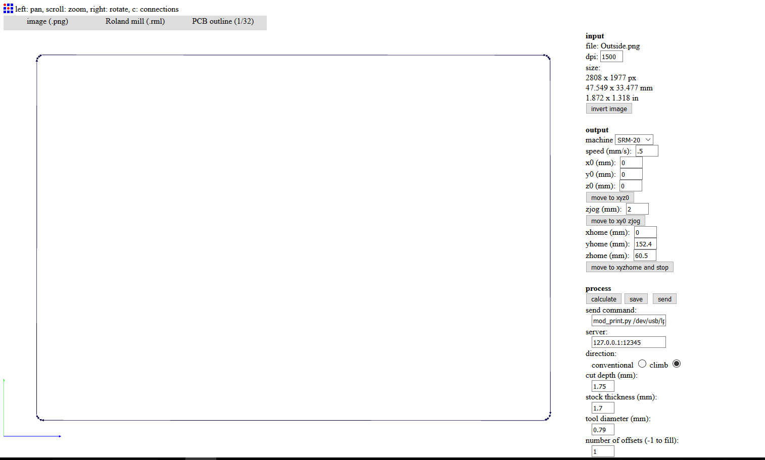
For outside cut draws a black rectangle around the circuit and erase all inside traces. Also save it as .png it looks like:
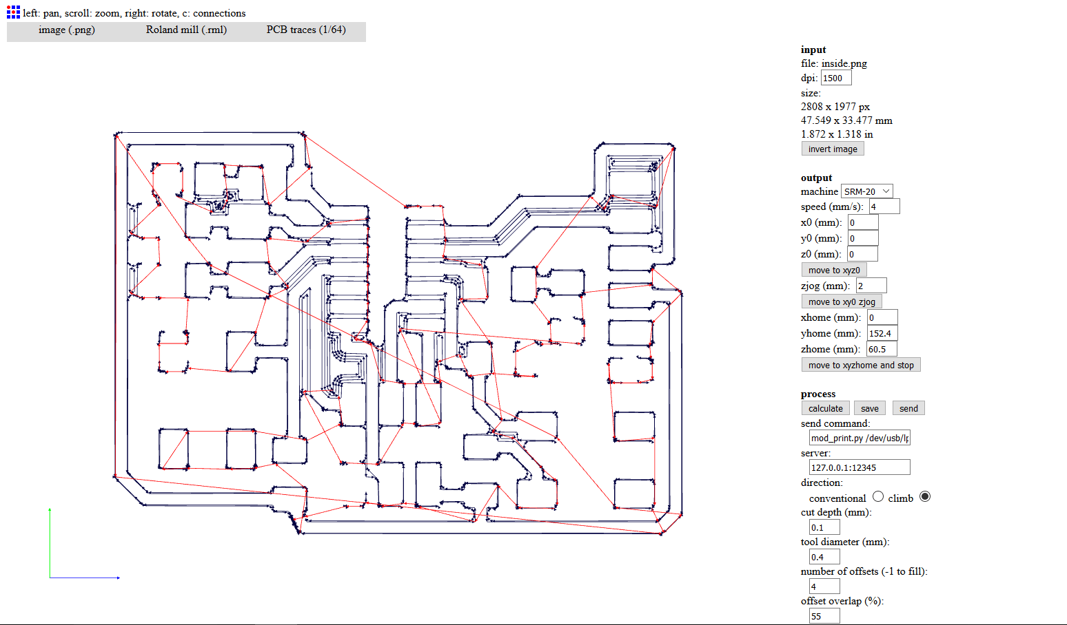
Now go to Fab Modules upload inside cut image with shown below settings, then save it as .rml
Do the same for outside cut
Step #7
Mill The PCB board
I followed the procedures of the Electronics Production Week. To mill my board I need two jobs first is inside cut for traces using 1\64" 0.4mm end mill tool. Second is outside cut for cutting the board borders using
1\32" 0.8mm end mill tool. Before I started I
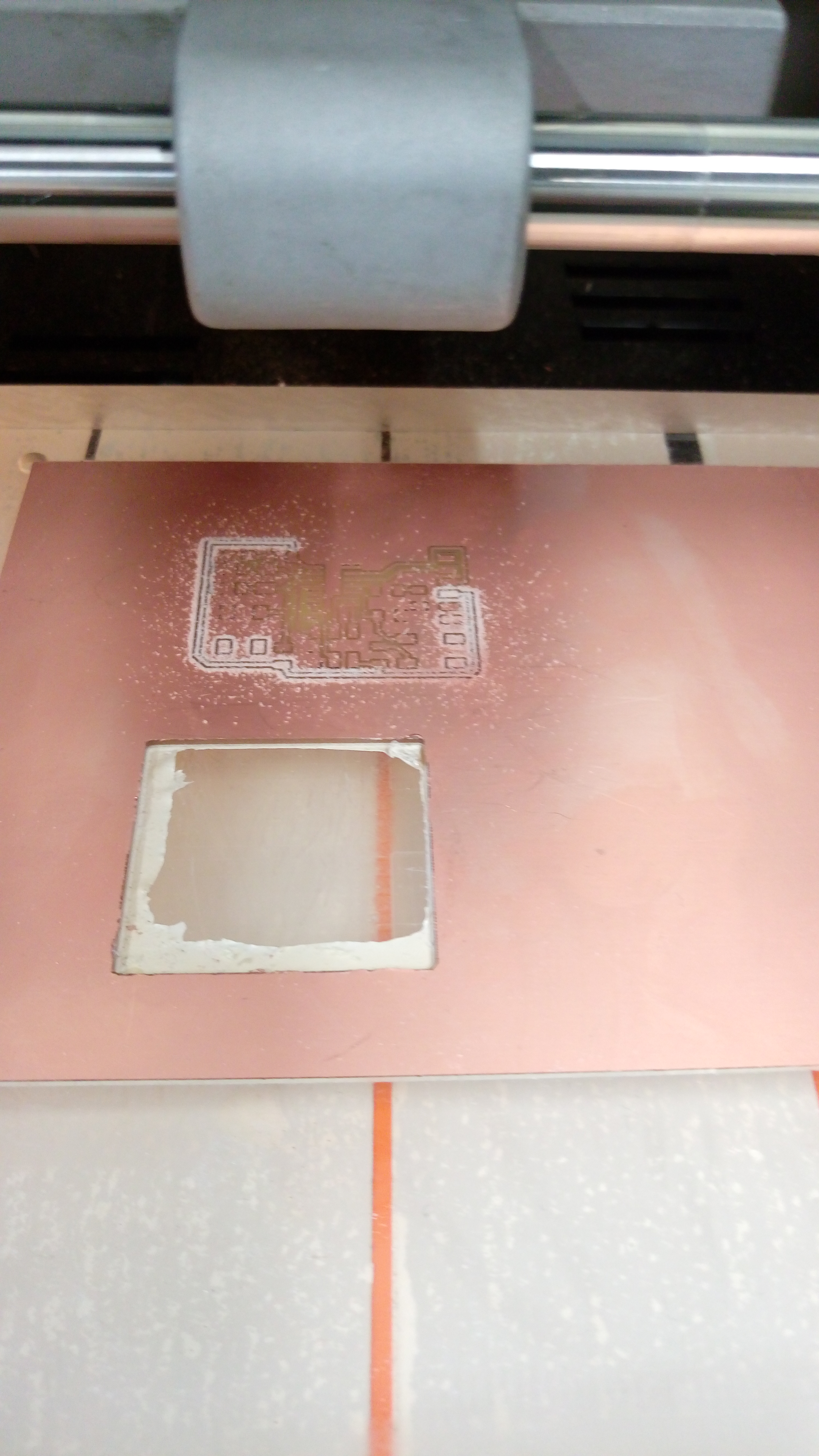
Set Z axis origin also X and Y origns. Then start the job on Roland machine.
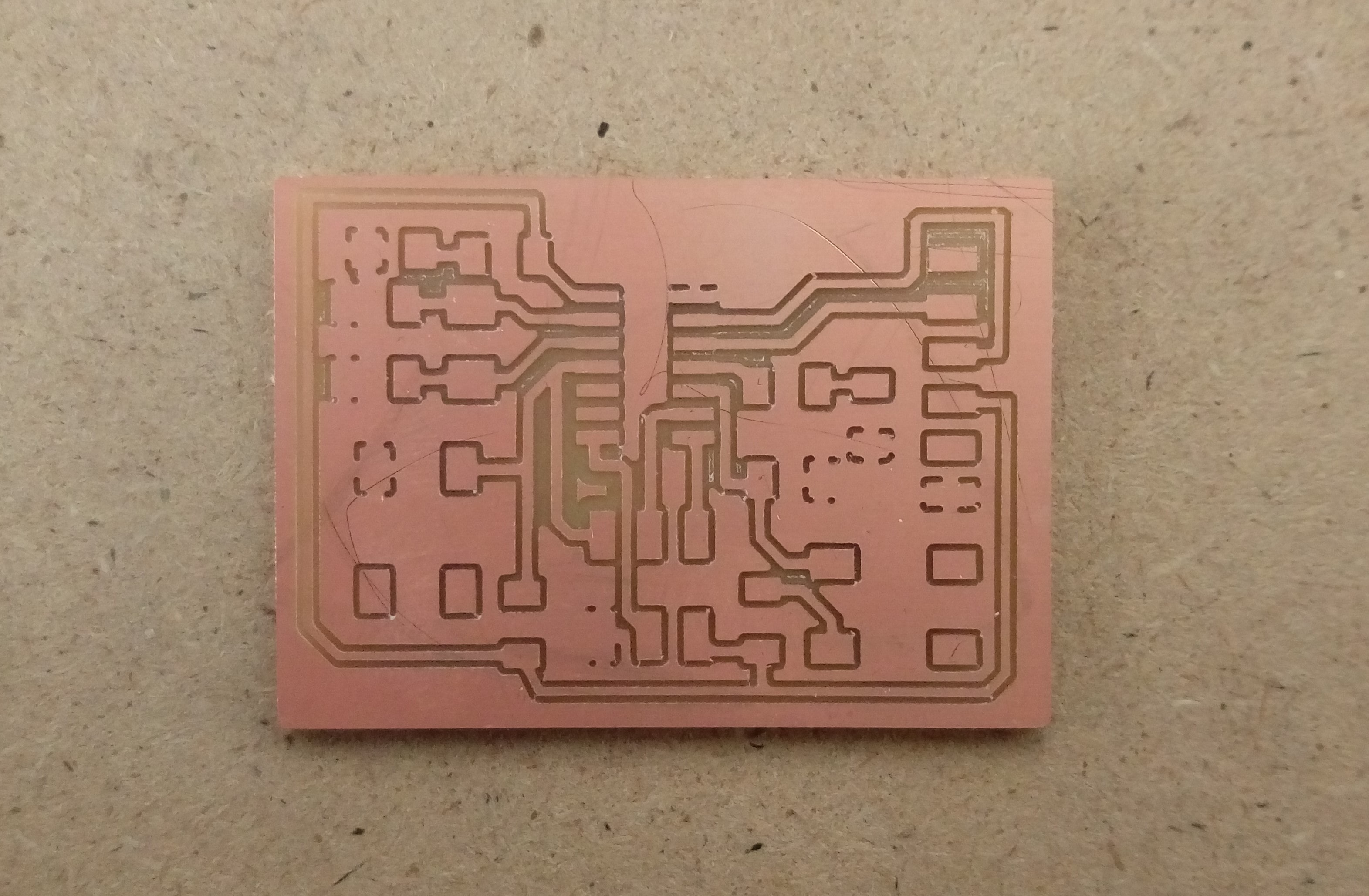
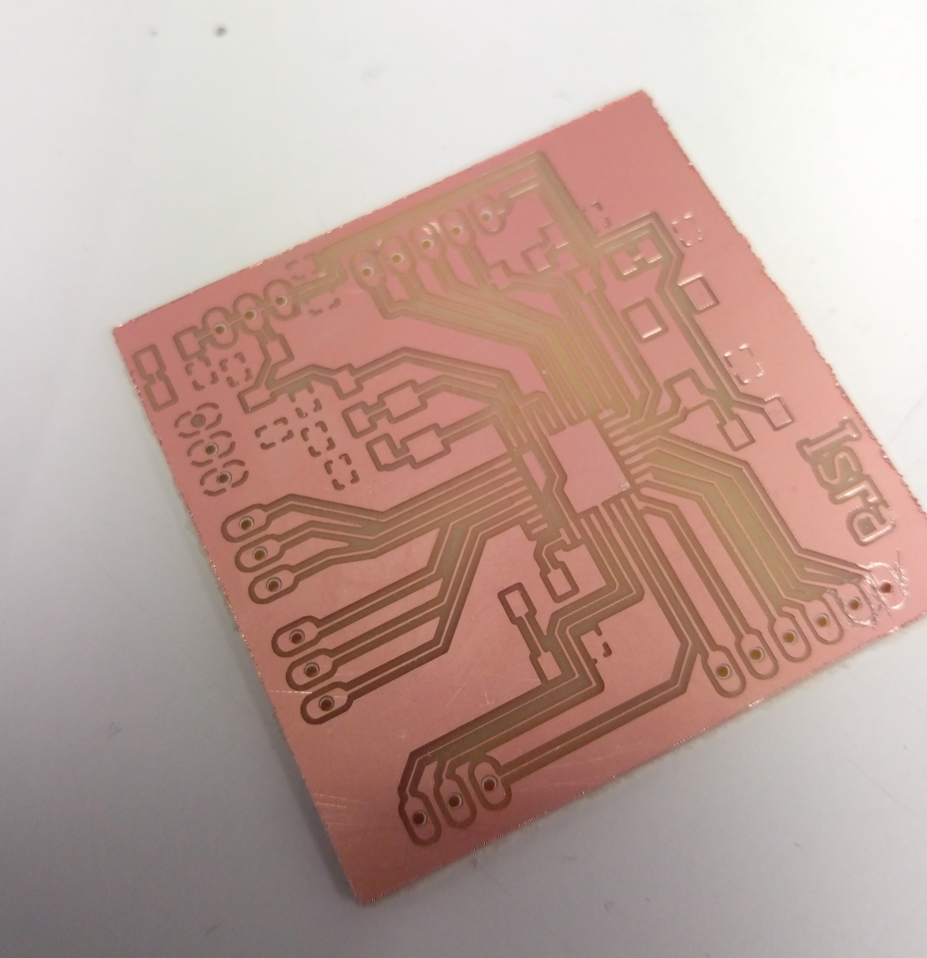
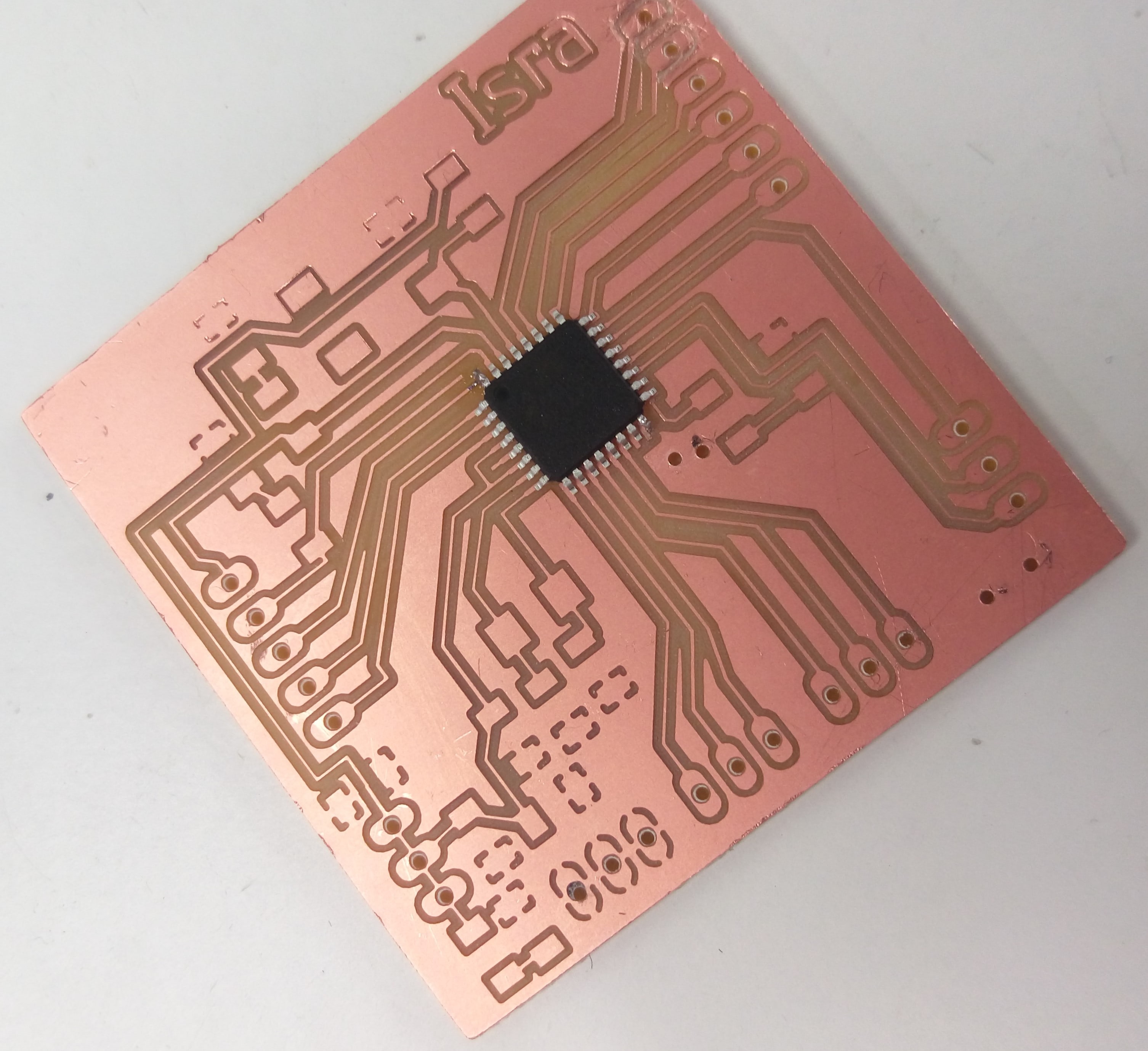
After I finally DONE!! my board looks like:
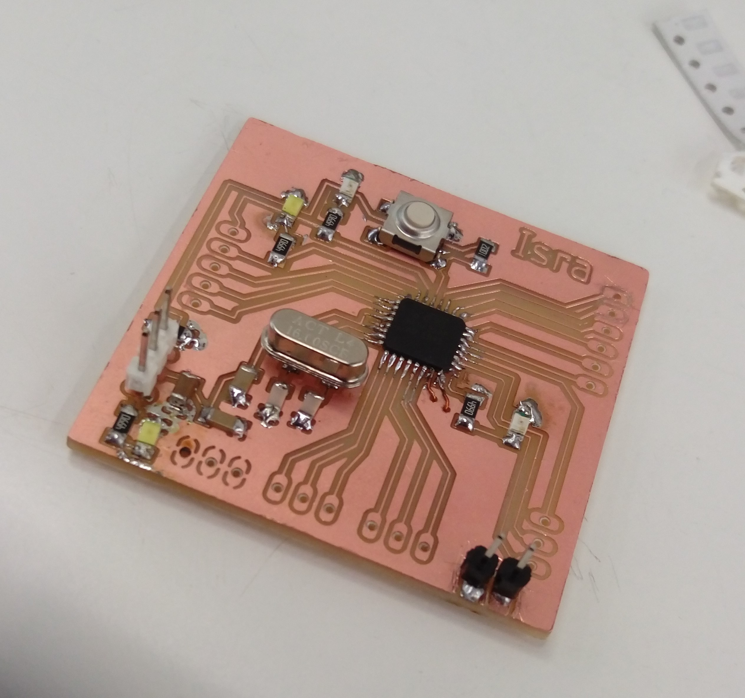
Step #8
Soldaring
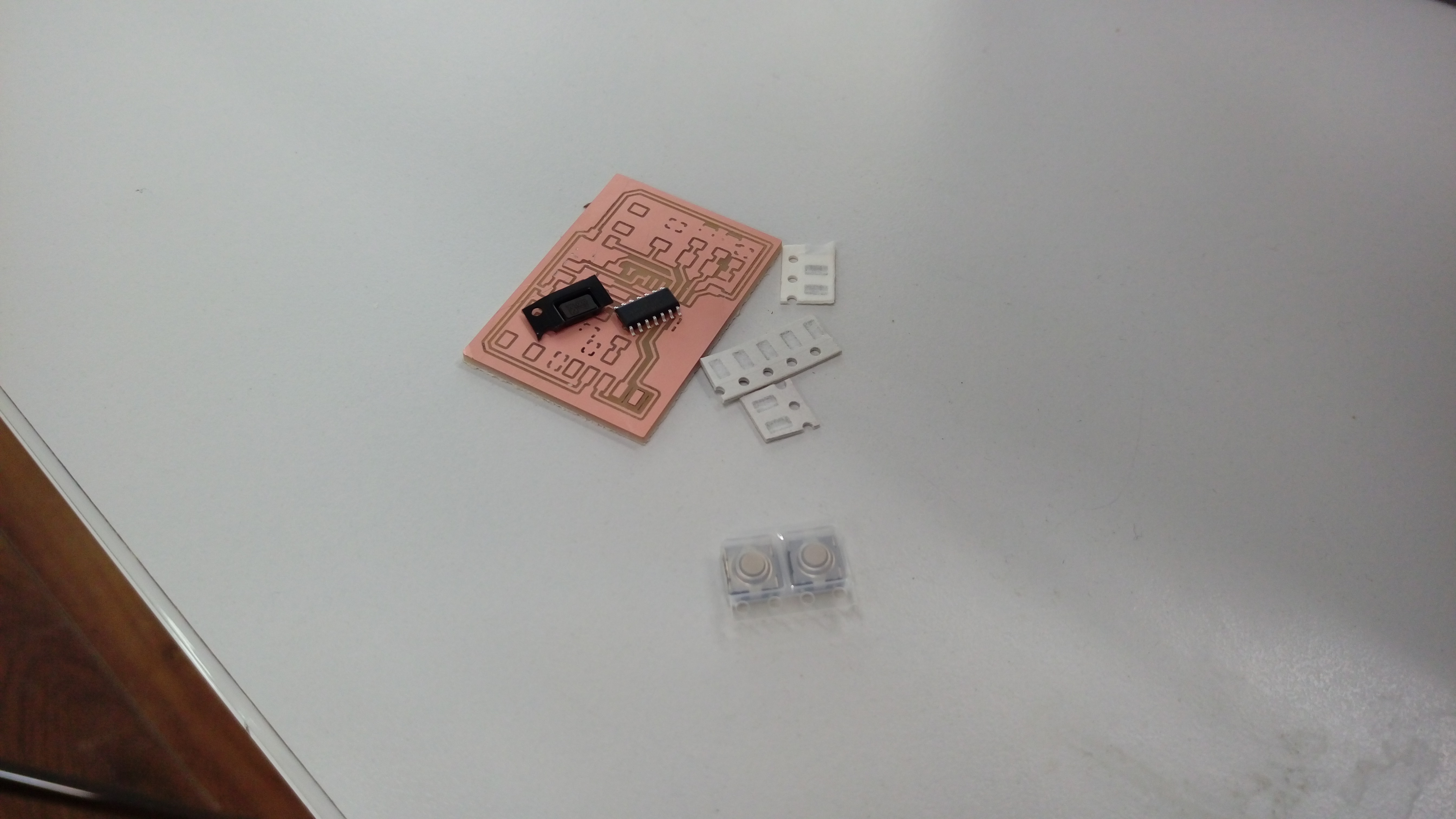
I prepared the components.
Then I took time to solder them ^_^ . I was faster than the previous week because I had a good experience in soldering now :p
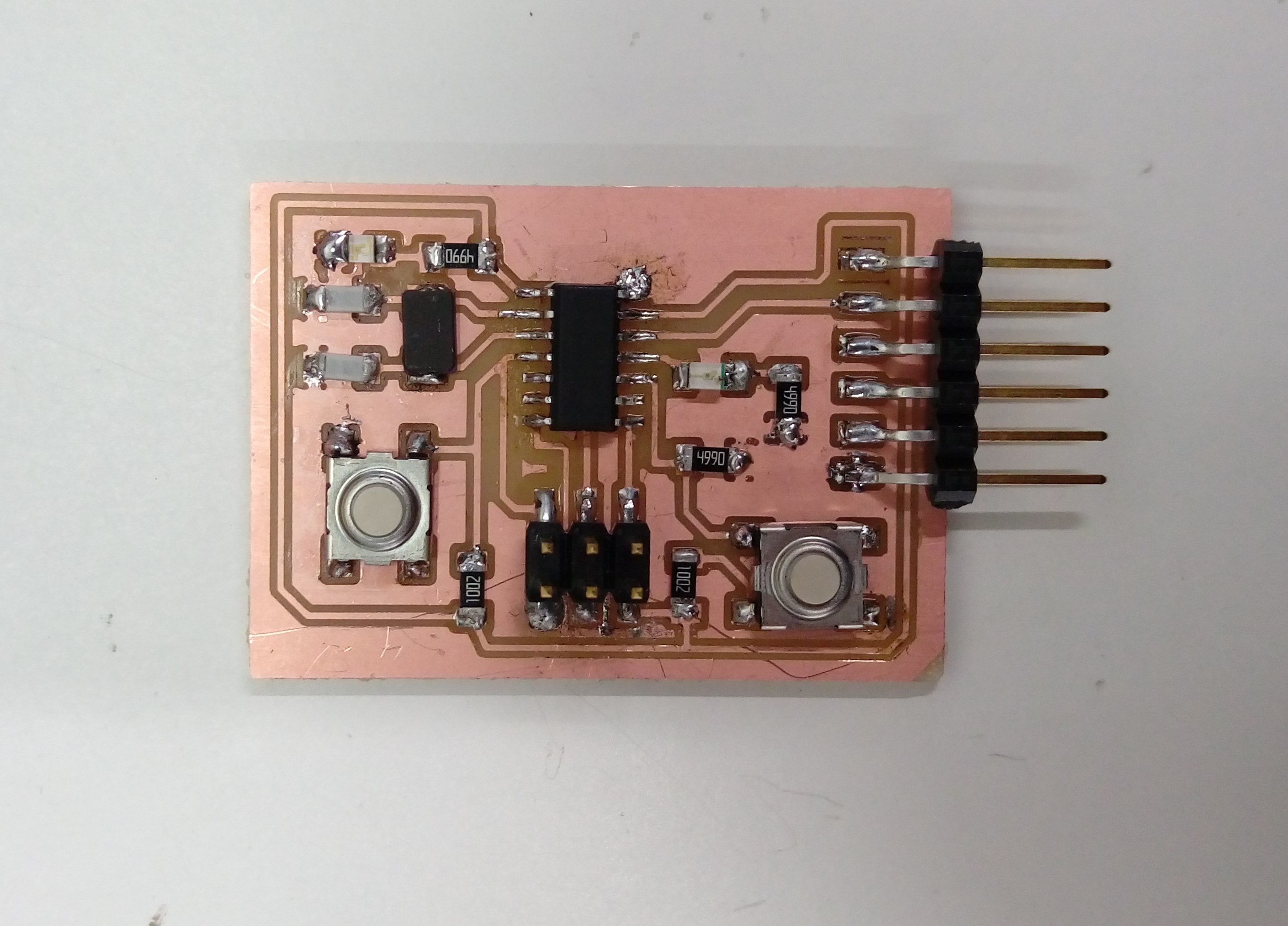
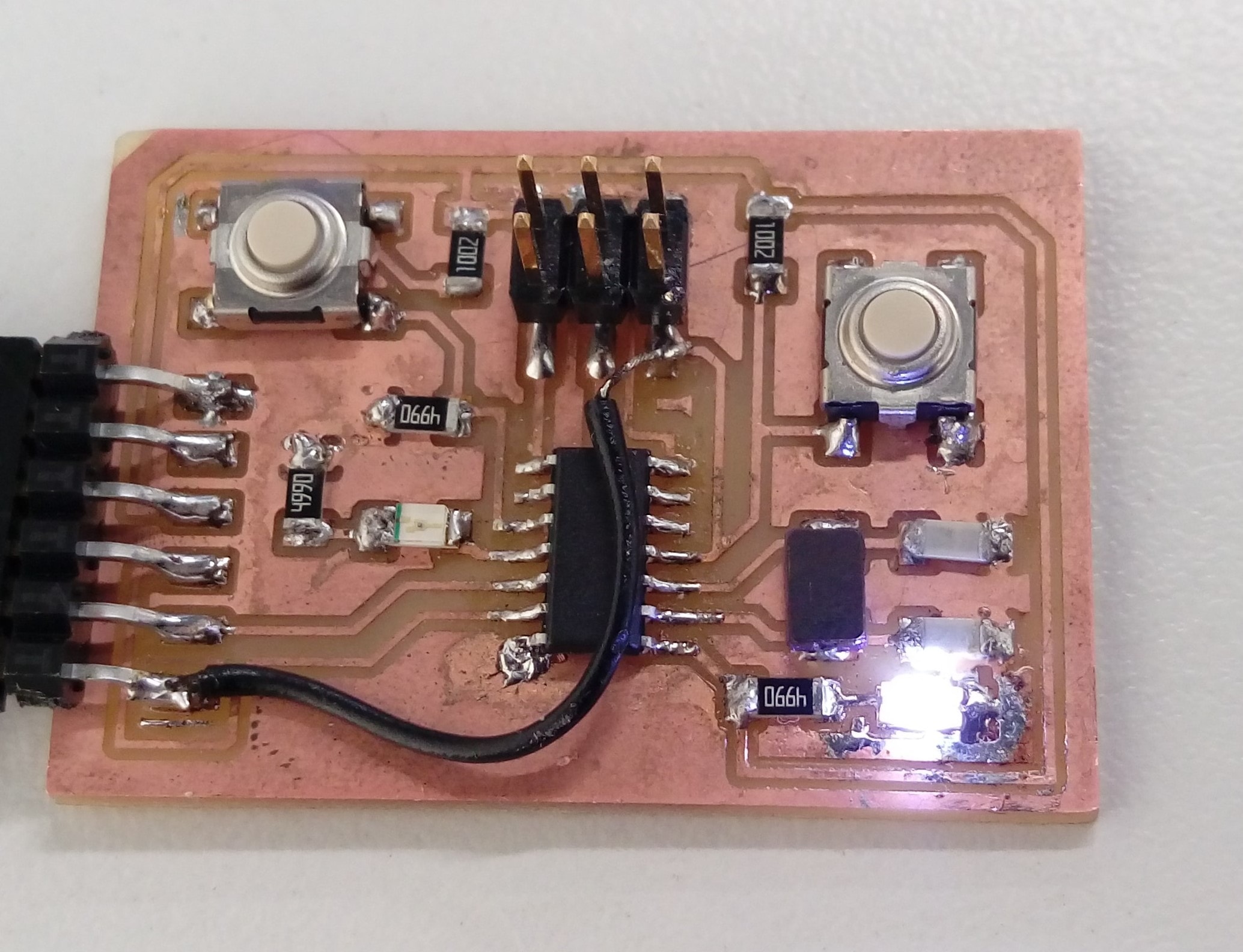
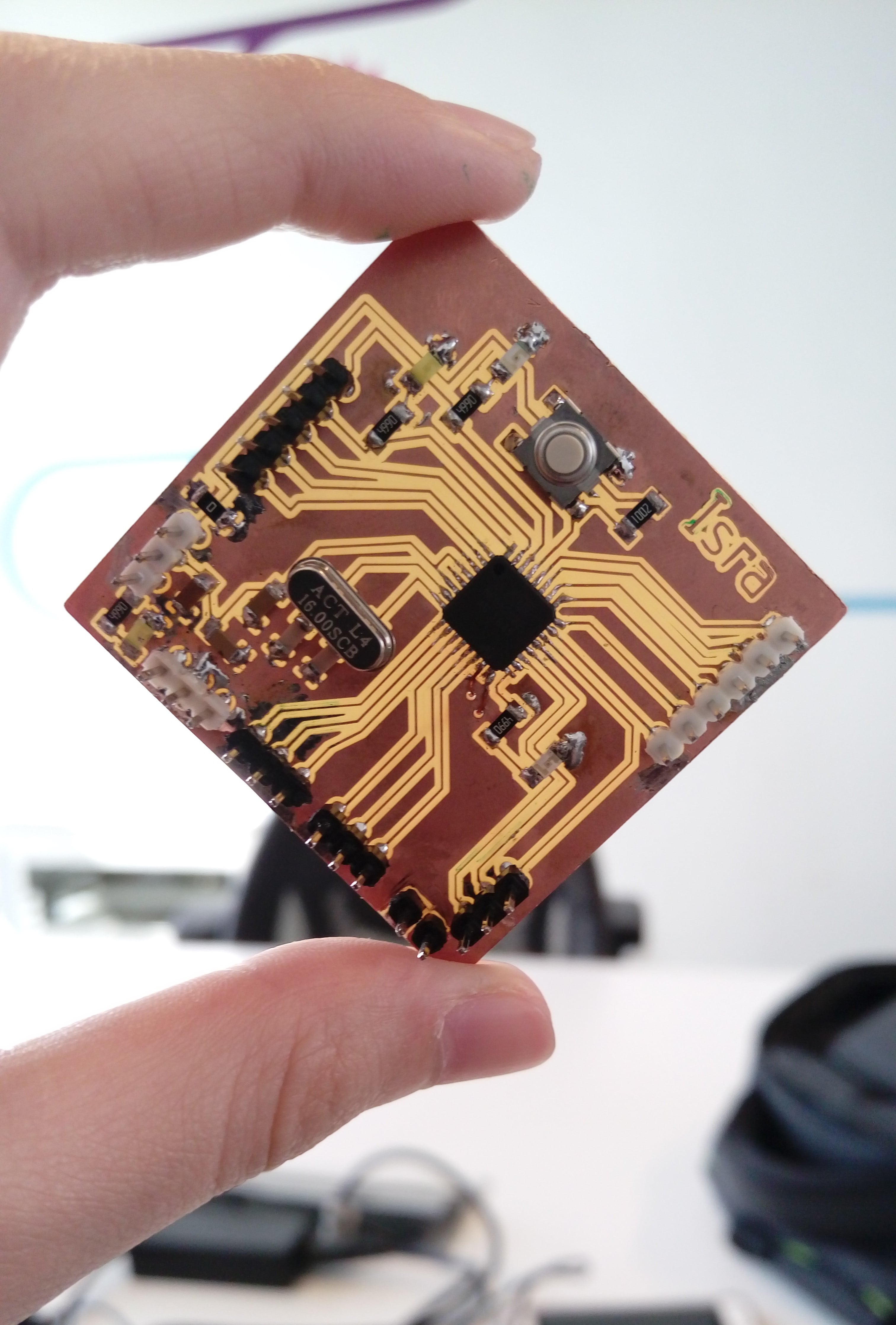
After I Finished soldering:
Step #9
Board programming using Arduino
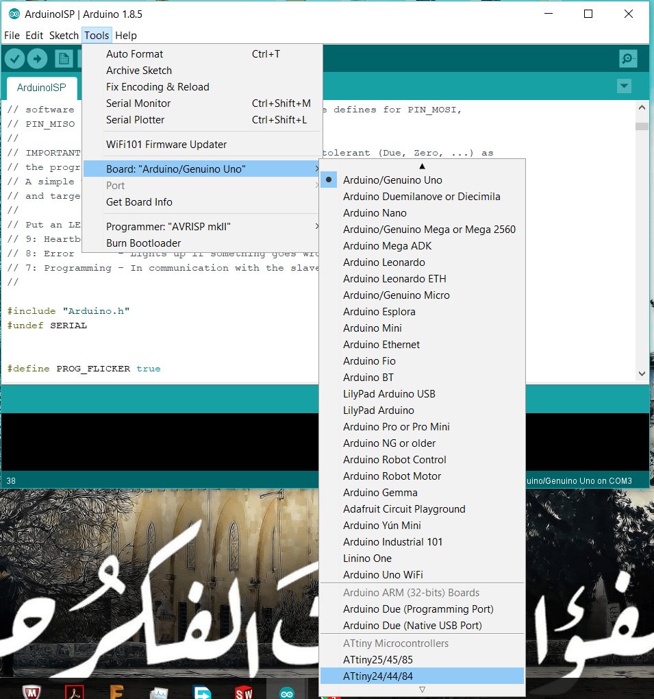
In this part I will use Arduino UNO board to program my board.
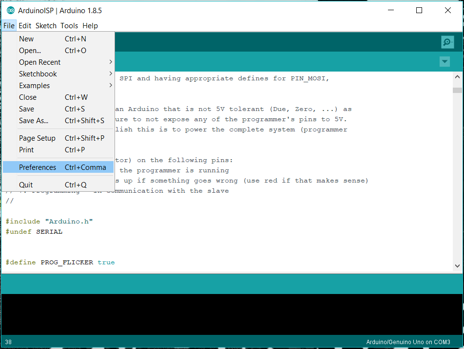
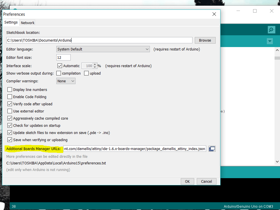
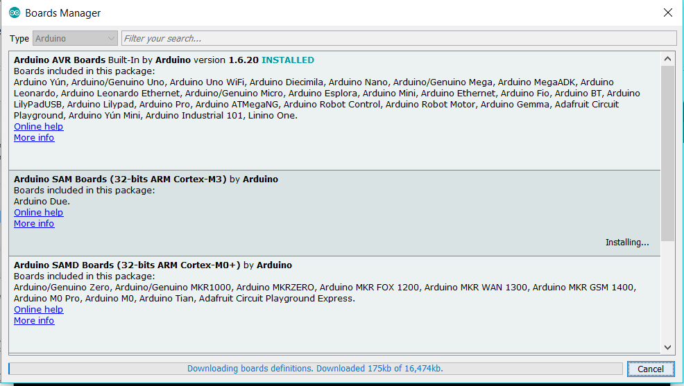
Start by installing a library to define ATtiny44 board in Arduino ID software follow
this tutorial
as shown in steps below:
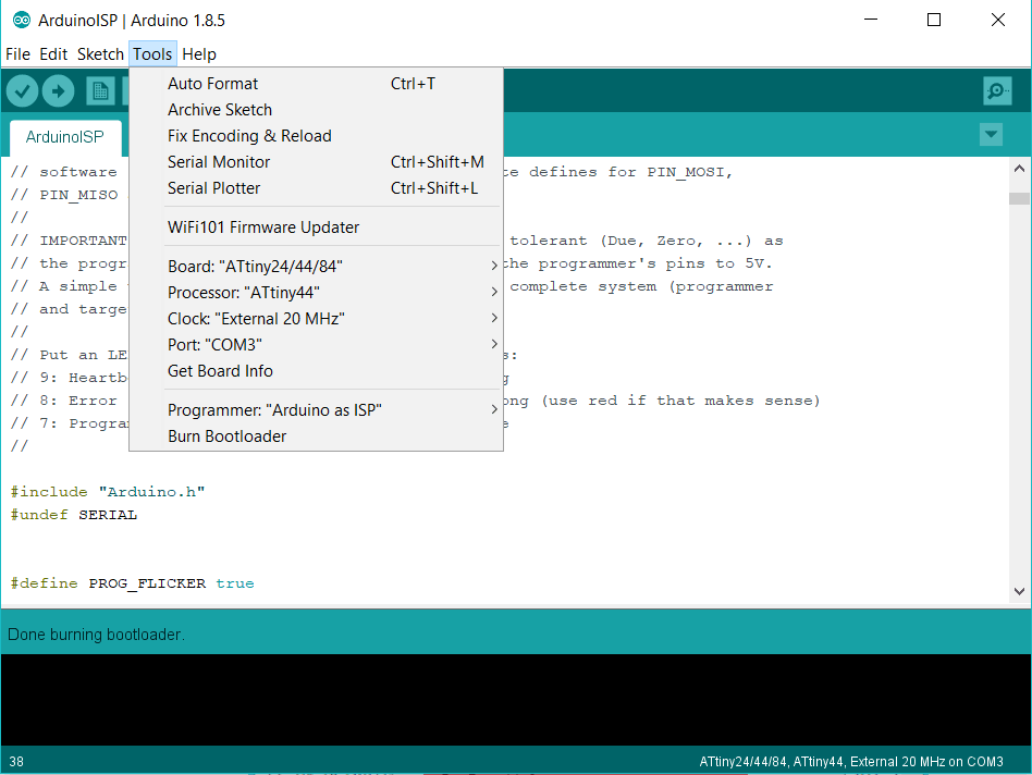
Now ATtiny44 in the board list choose it and select these settings
Now connect Arduino to computer and open ArduinoISP example then upload it to your arduino.
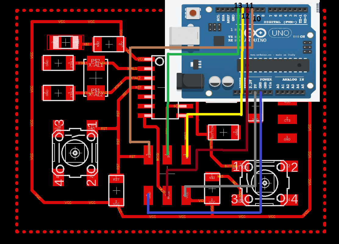
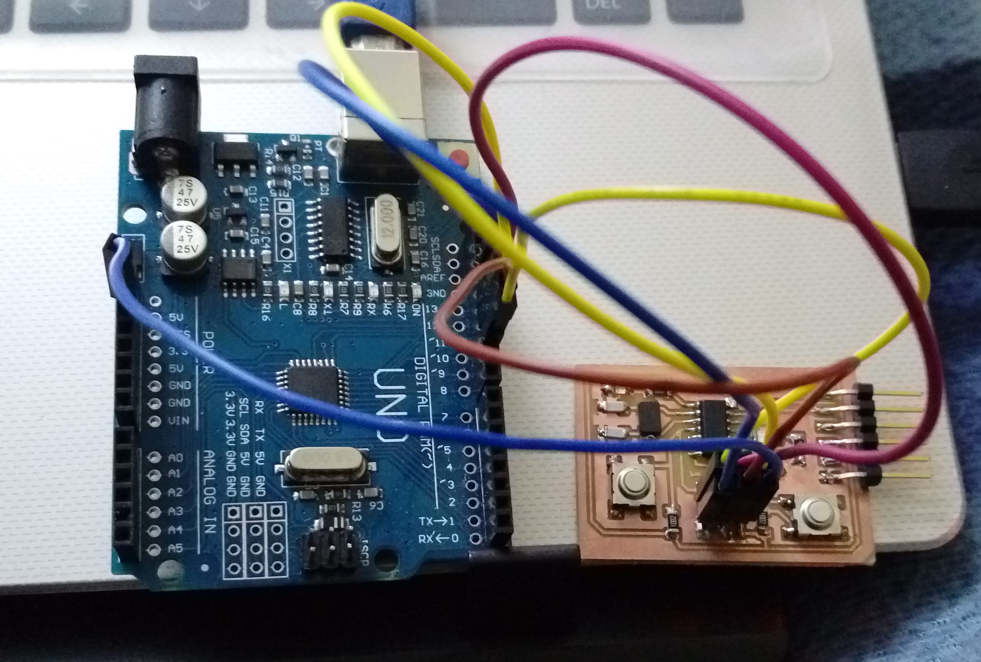
Then, connect the board ISP to Adruino as using this connection
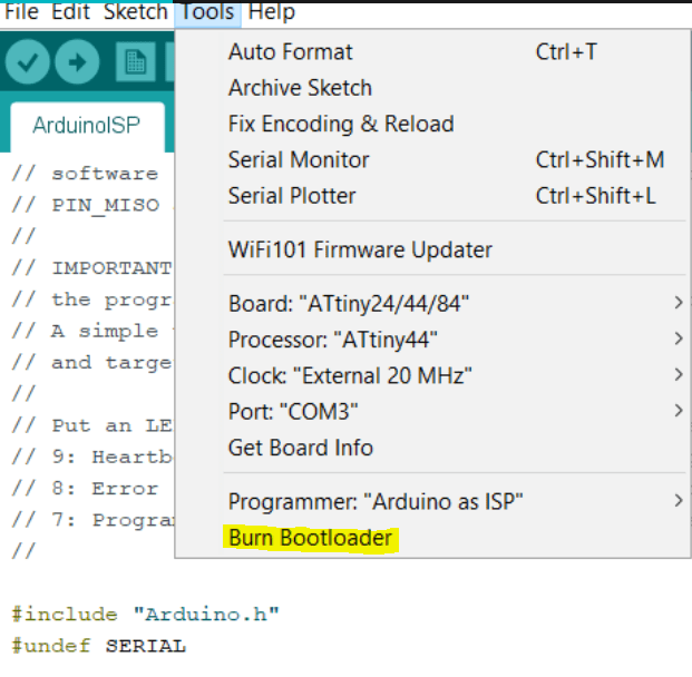
After connect the board to Arduino connect Arduino to computer then burn bootloader into your board as shown:
My board when connect to power ^_^ .
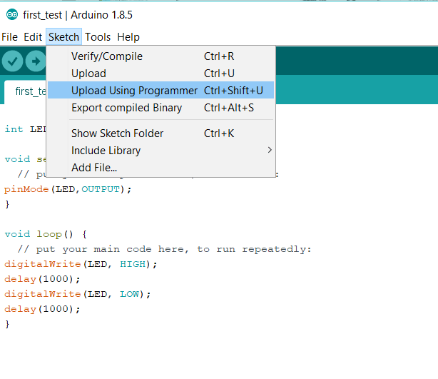
Write a code to upload it to your board, I wrote a code to blink a LED connected to pin 2 for 1 second. Then upload it as shown
upload it using arduino as programmer like this:
Finally it works!!!!!!!!!!!!
Watch the video
Problems and Solutions
Problem #1: Roland Misalignment
misalignment problem, because there is a misalignment in the Roland bed some traces didn't cut correctly as shown:
To solve this problem erase good traces from an image using GIMP software. The layout looks like the below image. Then repeat the process with fabmodules and milling again.
To make sure there is no connections between traces I used a digital multimeter's continuaty check option. I checked all traces before move to soldaring.
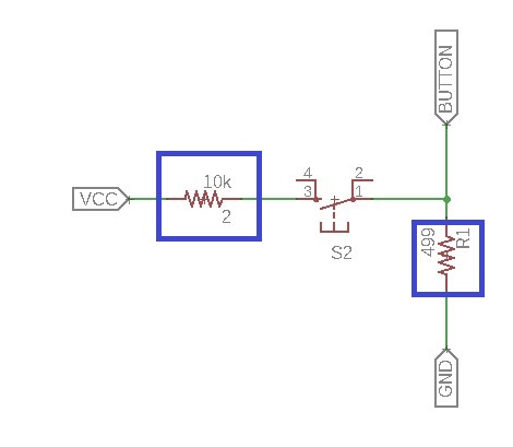
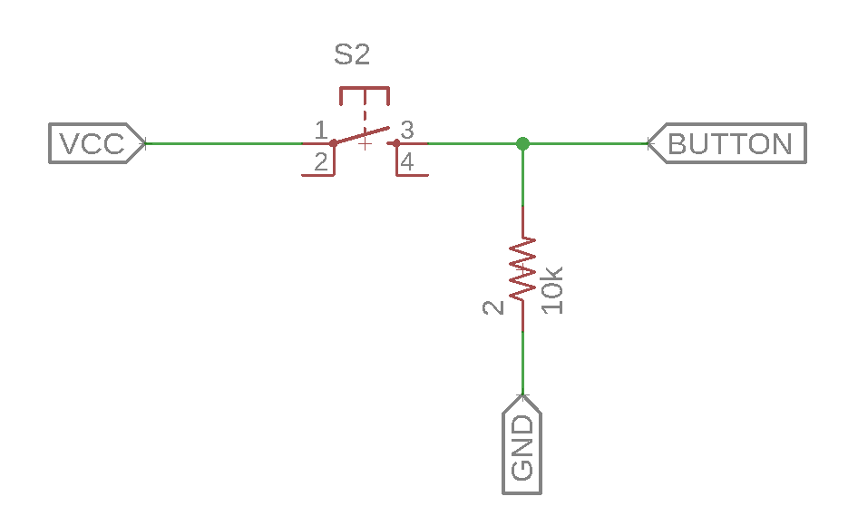
Problem #2: Wrong Button Design
It was my first time designing a schematic of a board, I lately discovered that I made a very stupid mistake. I wrongly connected two resistors with the Button:
I fixed my mistake and redesigned the button's schematic as shown:
Then I fixed board's layout
It was easy to fix the design on a computer, but to repeat the fabrication and soldering processes it will be time consuming, so I had a better idea, I replaced 499 ohm resistance with 10K ohm resistance, also I I replaced 10K ohm resistance with 0 ohm resistance as shown below, I think by this modification I solved the problem smartly ;)
Build my own general parpouse board
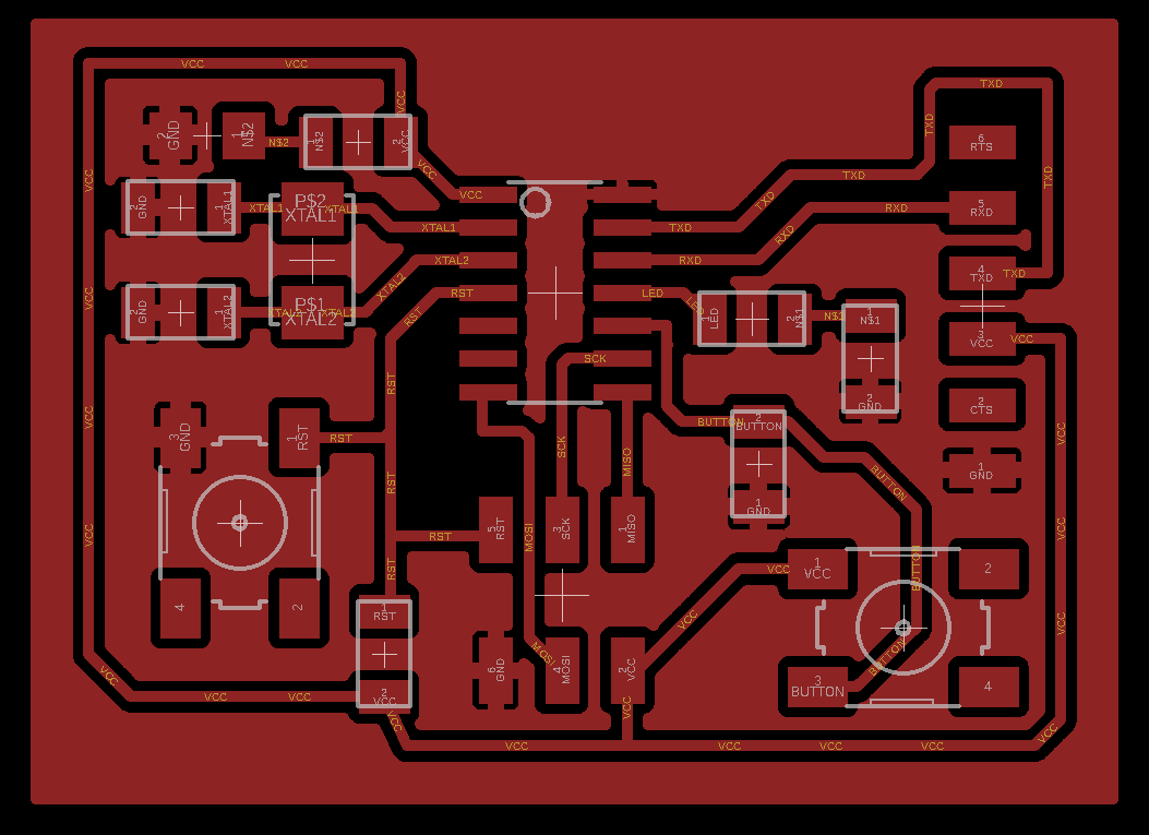
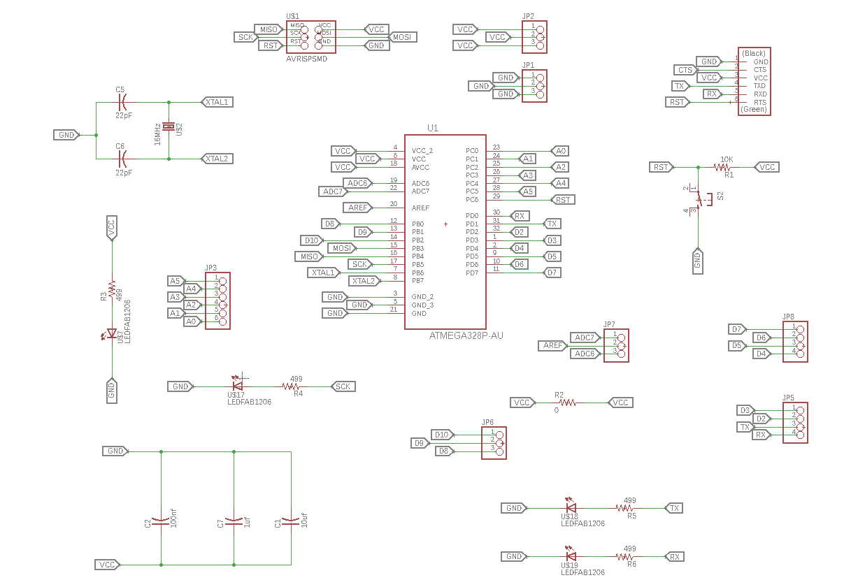
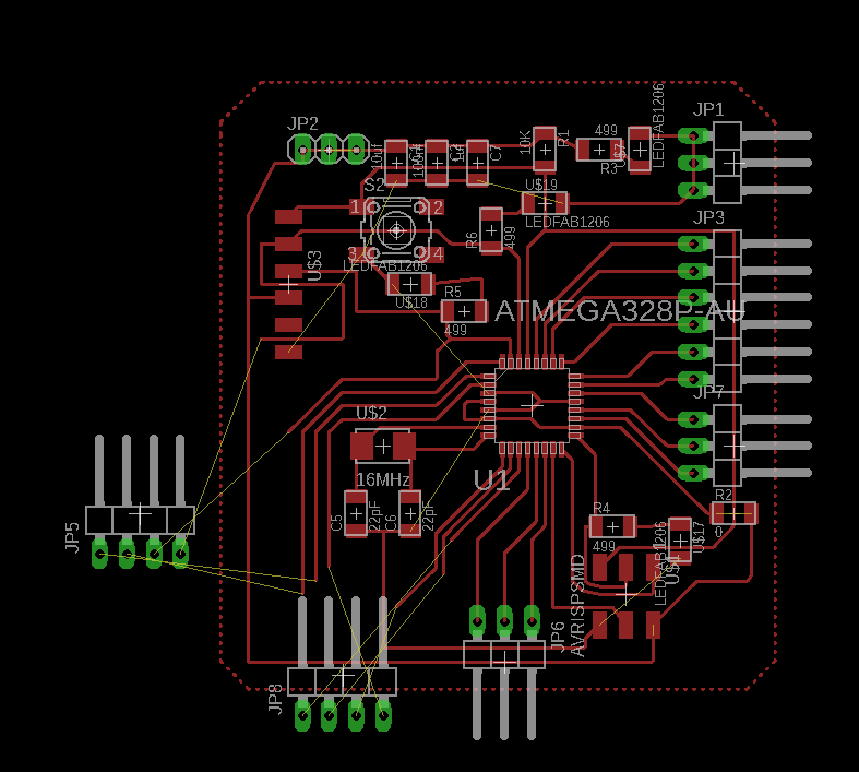
I want to design a general purpose board using Atmel ATMEGA 328p. General purpose board means a board could be used for many applications just like Arduino UNO. To do that I should connect ALL pins of ATMEGA 328p chip to a pin header so I could reach each pin when it's needed in specific applications.
The list of components:
ATMEGA 328p chip x 1
Cystal 16MHz x 1
Capacitor 22 pF x 2
Resistor 499 Ohm x 4
Resistor 10K Ohm x 1
Resistor 0 Ohm x 1
SMD Buttons x 1
Different LED x 4
Many male pinheaders
This is my schematic:
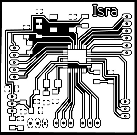
I stick in this step for a long of time repeating routing for more than 5 times
Then I decided to remove the AVR ISP pin header also breaks other pin headers into just three pin header instead of four or six. After several tries I finally success!
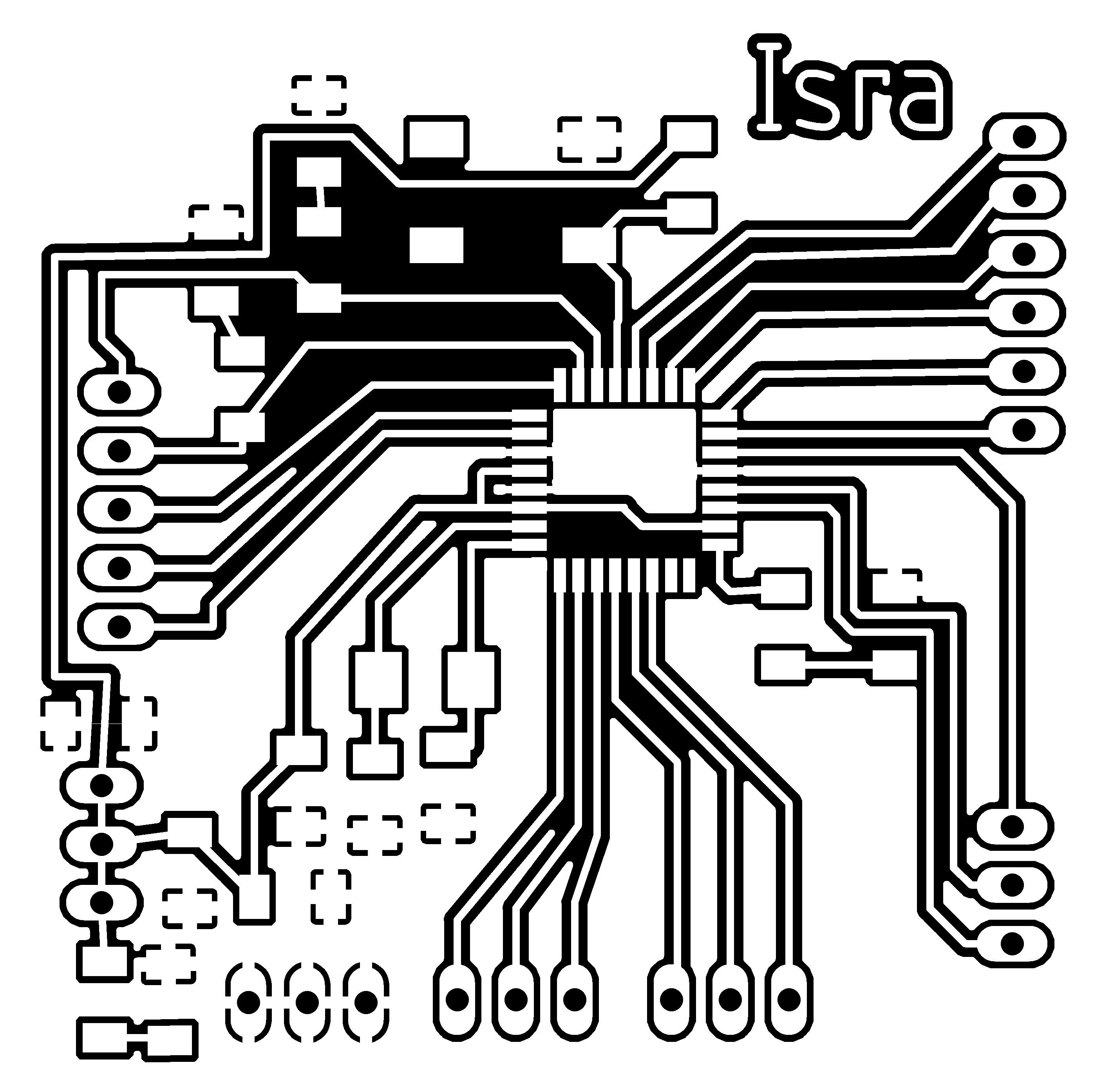
To mill this board I made 3 separated jobs following exactly previous steps in Electronics Production Week.. Firat job was inner cut. I used ball nose 1/64''
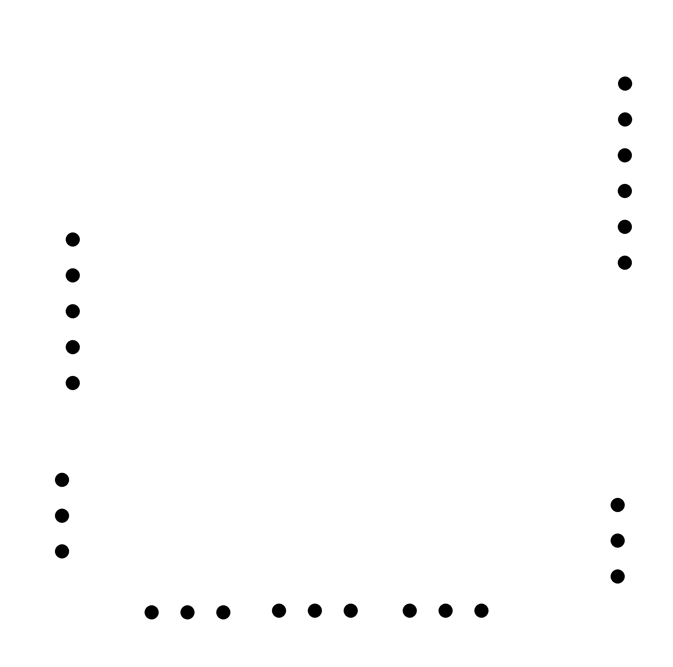
The second job is to drill the holes. I just expodted the Pads layer and sent them to GIMP 2 software to remove the text from each hole and make them black as shown in final .png picture. Then I uploaded it to the fab modules.
The final job is simply the out cut.
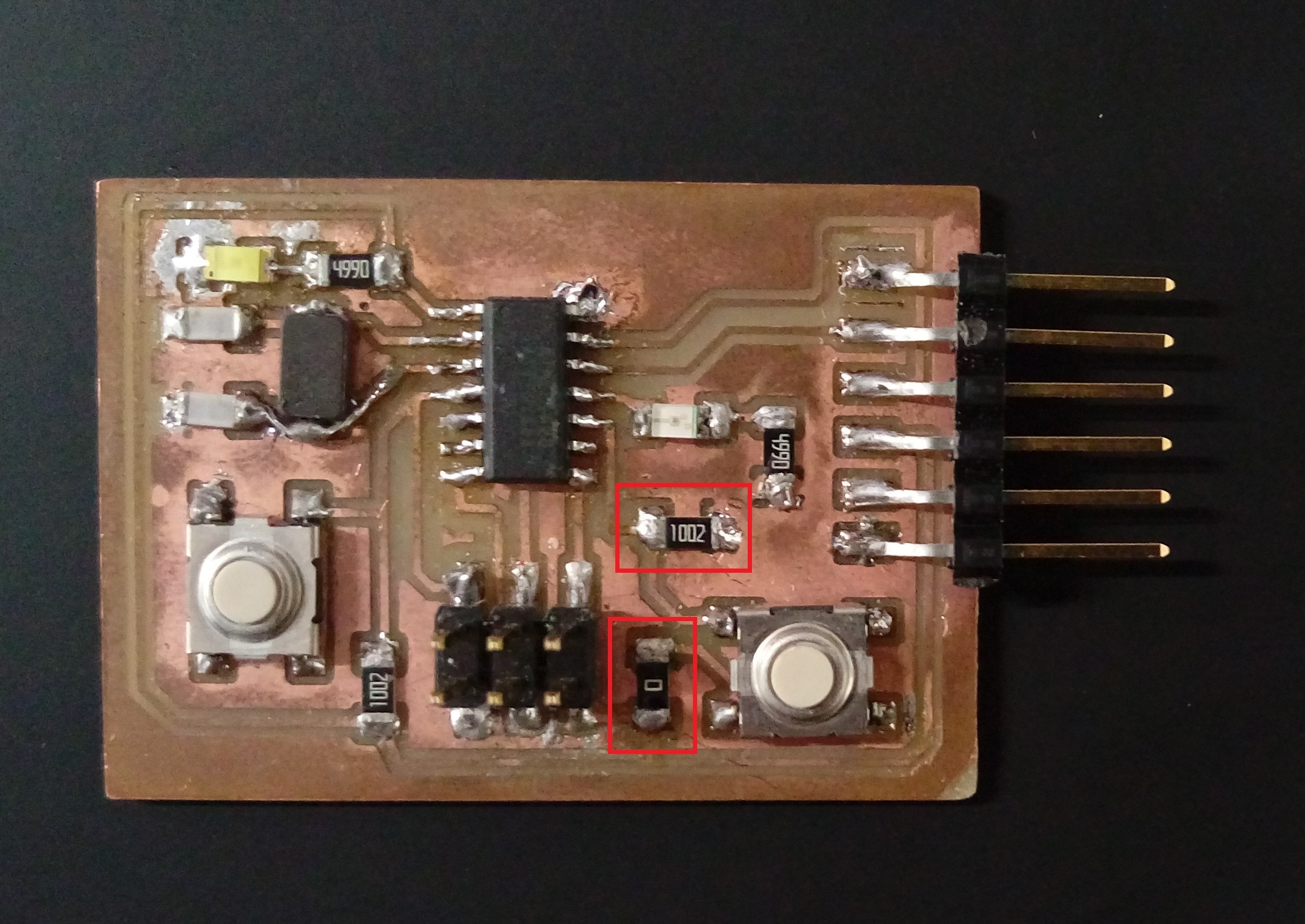
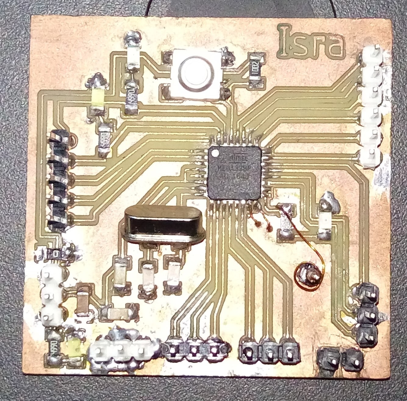
My board after milling is finished looks like:
Soldaring steps:
This is my final Adruino board
Problems and Mistakes in General Purpose Board
As I said before, I spent a lot of time in routing my Arduino board and then I deleted the ISP pin header. By this trick I solved the problem of routing, but I made a very stupid and critical mistake I forgot to connect 3 pins which don't connect to other pin headers so I couldn't reach them anymore, those 3 pins were MISO,MOSI,SKI so I will never be able to program my board. I just want to throw it away and cry!!!! But then I decided to connect them manually and test my design if there is time in next weeks I will repeat it again.
This is missed pins:
I used Roland machine moved X and Y axis manually to the desired space, fixed Z axis zero, then turn spindle on and slowly drop the Z to -1.8mm (The thickness of PCB board).I made two holes using this method, then soldered thin copper wires to connect MC pins with pin headers.
My arduino after fixed shown below 'it need to be tested'