Electronics Design Week
Two weeks ago, we learnt how to produce a PCB using a ready design so basically we only had to mill the board and solder it's components.
This week, we have to redraw the Echo Hello Board adding at least a button and LED.
Creating the Schematics
For this week's printed circuit board design, we need to choose a software to use. I decided to use  Eagle from Autodesk.
In Eagle you have to first create a Schematic for your circuit board. A schematic is basically a layout of the components you will be using and how those components are connected to each other.
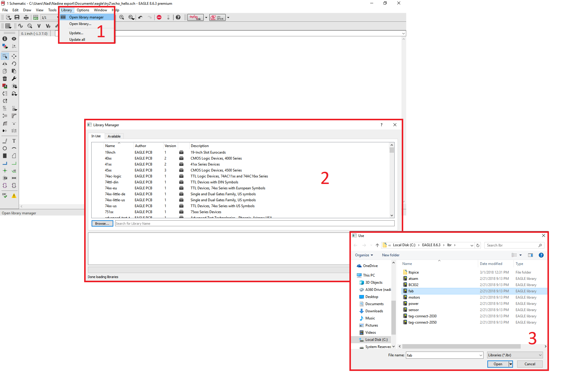
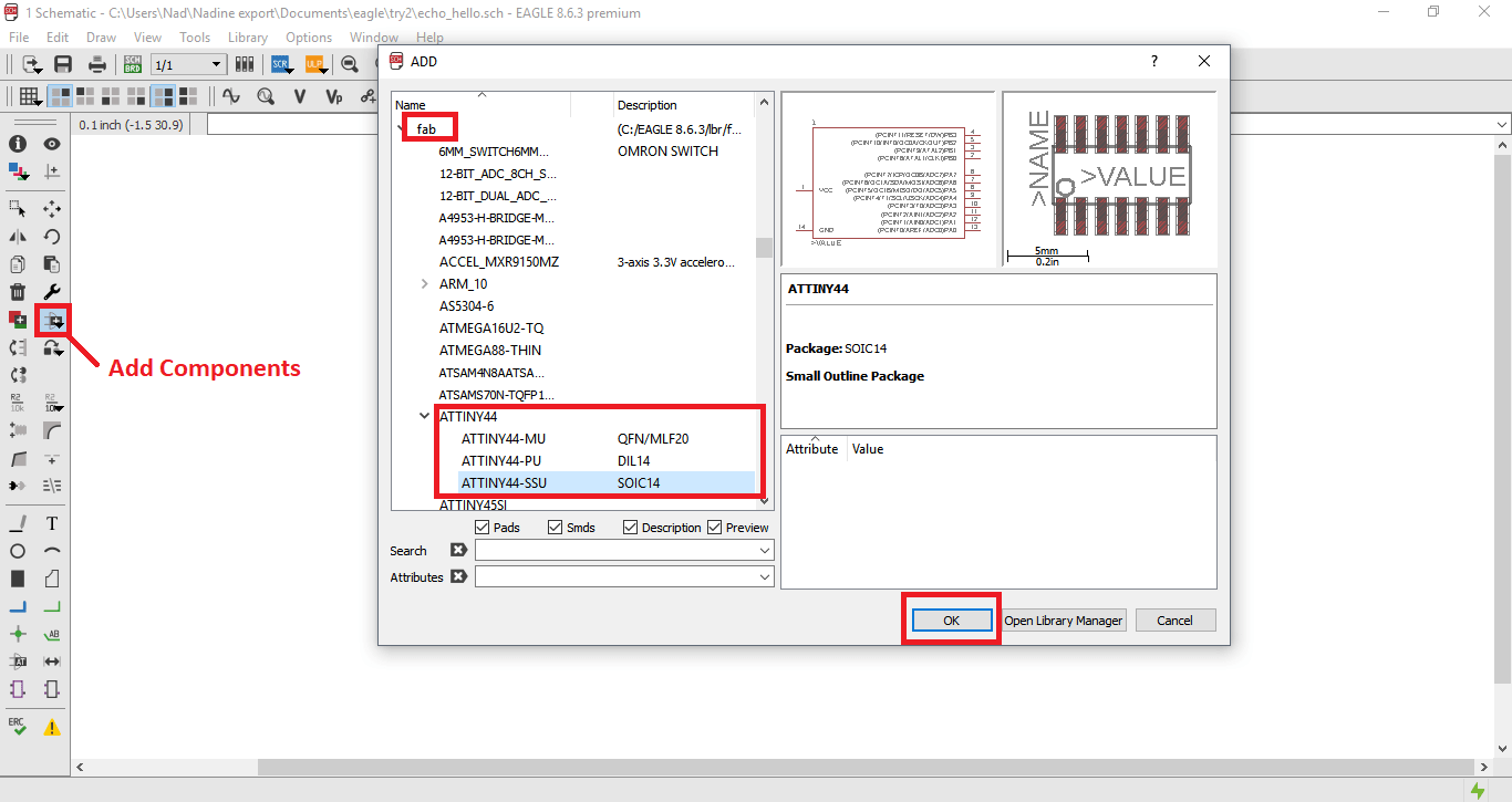
First I downloaded the Fablabs Library and started adding the components I needed.
I used a lot of Labels to avoid having wires all over the place which will confuse me.
We will be using an Atmel board. The same one we used on Electronics Production week which is the Attiny44.
To understand where I'll be connecting the additional components, I took a look at the Attiny44 Datasheet. The pinout is shown below.
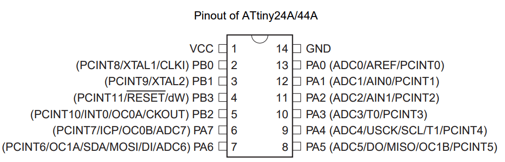
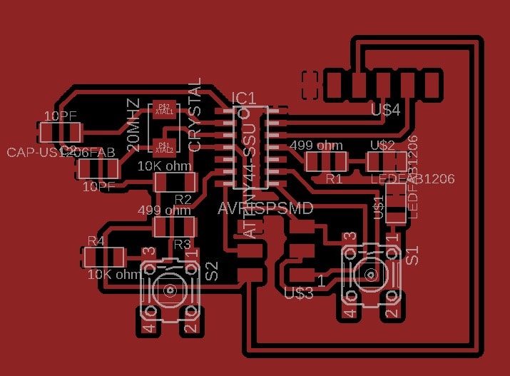
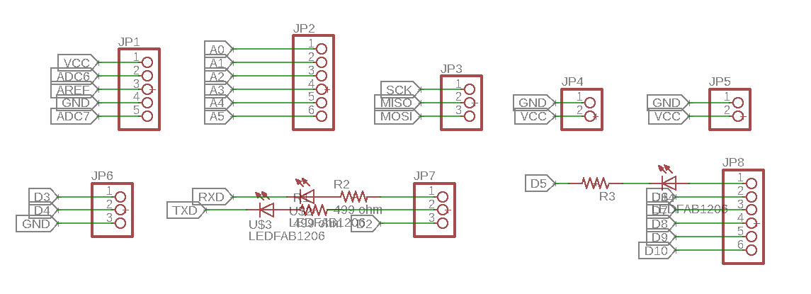
Refrencing the above pinout, I created the below schematics for my board.
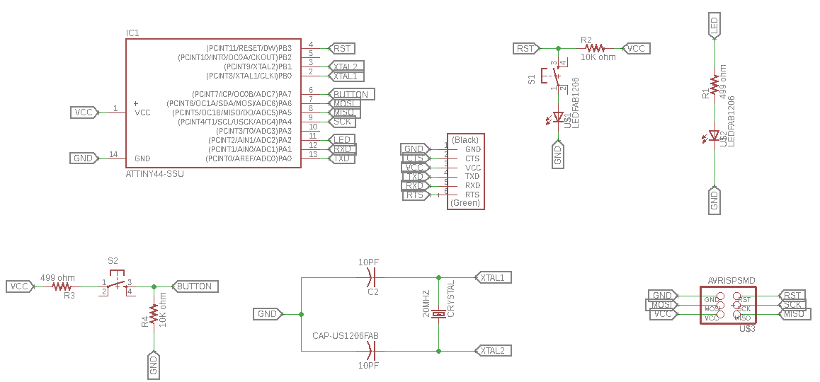
Here are the connections to the microcontroller.
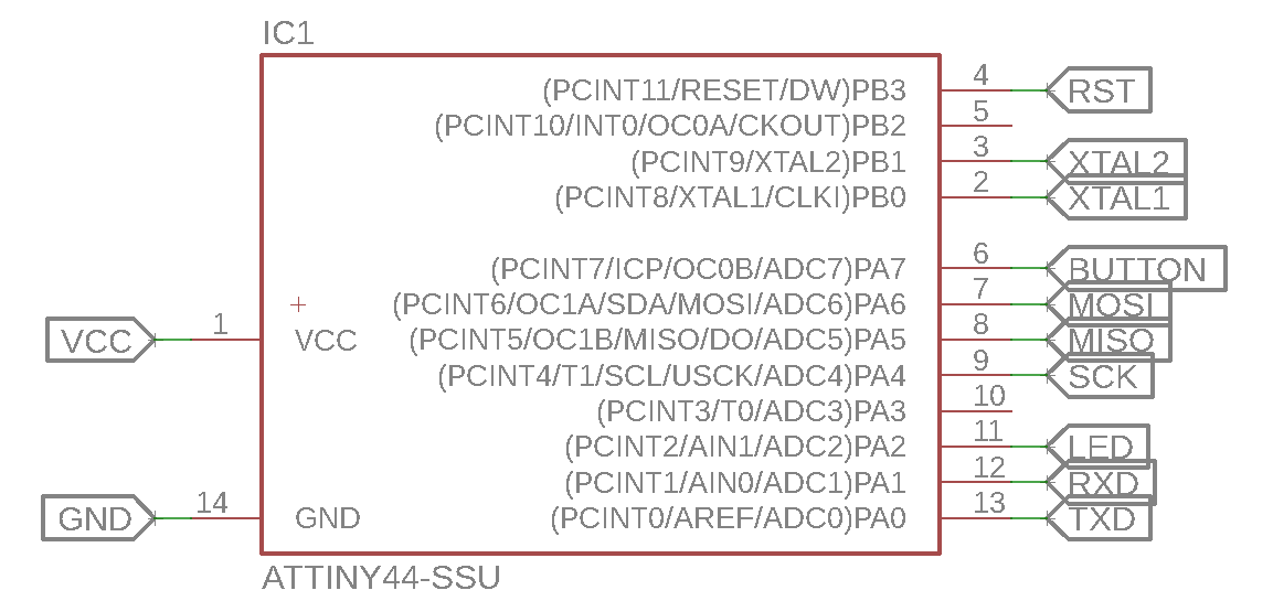
Each microcontroller has a processing speed (instructions per second). It also has an internal clock but to make the microcontroller more precise, we connect it to a Crystal Oscillator.
Based on the above pinout, the crystal connects to pins 2 & 3.
The crystal we'll be using is a 20MHz Crystal.
Crystal manufacturers normally cut and trim their crystals to have a specified resonant frequency with a known "load" capacitance added to the crystal. Which means to have the crystal operating at the specified frequency you add the recommended value of capacitance.
For the 20MHz Crystal that we used, the recommended capacitance value is 8 PF, but that's harder to find so we used what's available in the fablab inventory which is 10 PF.
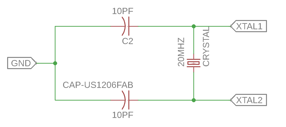
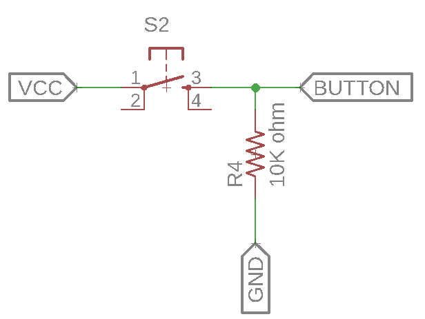
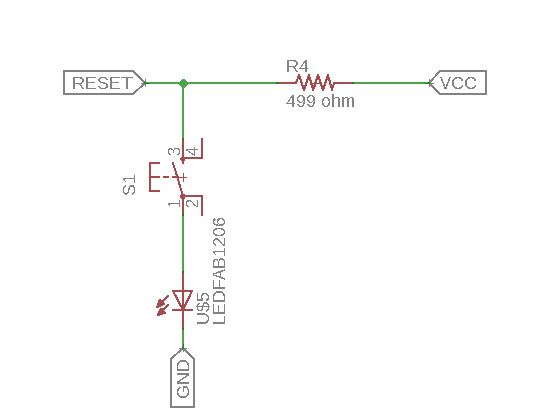
I decided to connect a Reset Button and have an LED light up when it's pressed. Looking at the pinout I figured out that it should be connected to Pin 4 of the attiny44.
The circuit of the reset button is shown below.
The reset pin is high when the switch button isn't pressed. When the button is pressed, the current will flow through the other branch and not into the reset pin; causing the pin to become LOW and the LED to light up.
I also decided to add another button so I could read it's state as an input and do a certain action when it's pressed. I connected that button to pin 6 as seen below.
With this circuit, I decided to do the opposite of the reset button. The pin (pin 6) is LOW when the button isn't pressed. The value of it becomes HI when the button is pressed.
The 10K Ohm resistor here is called a Pull-Down Resistor since it pulls the value of the pin to zero when the button isn't pressed. After thinking about this schematic, it would probably work just fine without the 499 Ohm resistor that I used to limit the current.
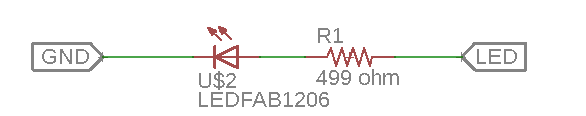
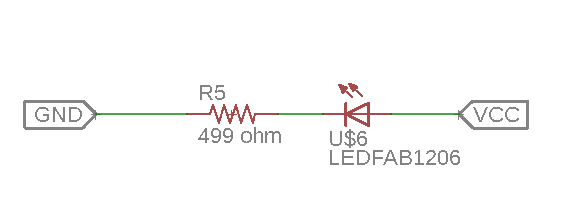
I also decided to add another LED that I can control through code.
I decided to connect it to pin 11.
The LED will light up when that pin is set to HI. The 499 Ohm resistor is a current limiting resistor used to reduce the current passing through the LED to avoid frying it. The minimum value for the current limiting resistor is 80 Ohm to limit the LED input voltage to around 2 Volts which is the foward-biased voltage of the LED which corresponds to the current rating.
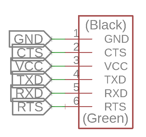
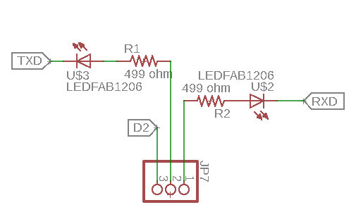
Next, I added an FTDI SMD-Header, I will connect the FTDI cable with this header to have my board talk to my computer serially. Since there's going to be communication going on between the board and the computer, there must be a transmitter (TX) and a receiver (RX). Looking back at the pinout, I decided to connect them to pins 11 & 12. These pins are not really built for serial communication but you can define them to act as a receiver and transmitter through code. The RTS and the CTS pins are not connected to anything.
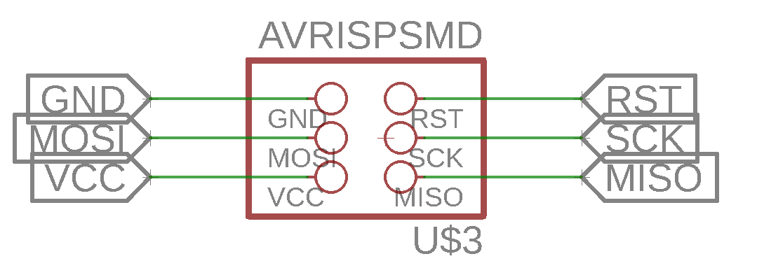
The only thing that's left is the connection between this board and the ISP we created 2 weeks ago. These header are ment to program our board.
This was all the easy part! Next we get to Board Design.
Board Design
In the board design window, you get to choose where you want your compoonents to be and how to route the traces. Here you will design the exact board that will be milled using the desktop milling machine.
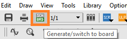
To generate your board design, just press the Generate/Switch to board button in the schematic window.
When you press yes, all the components are shown outside the black area all tangled togehter.
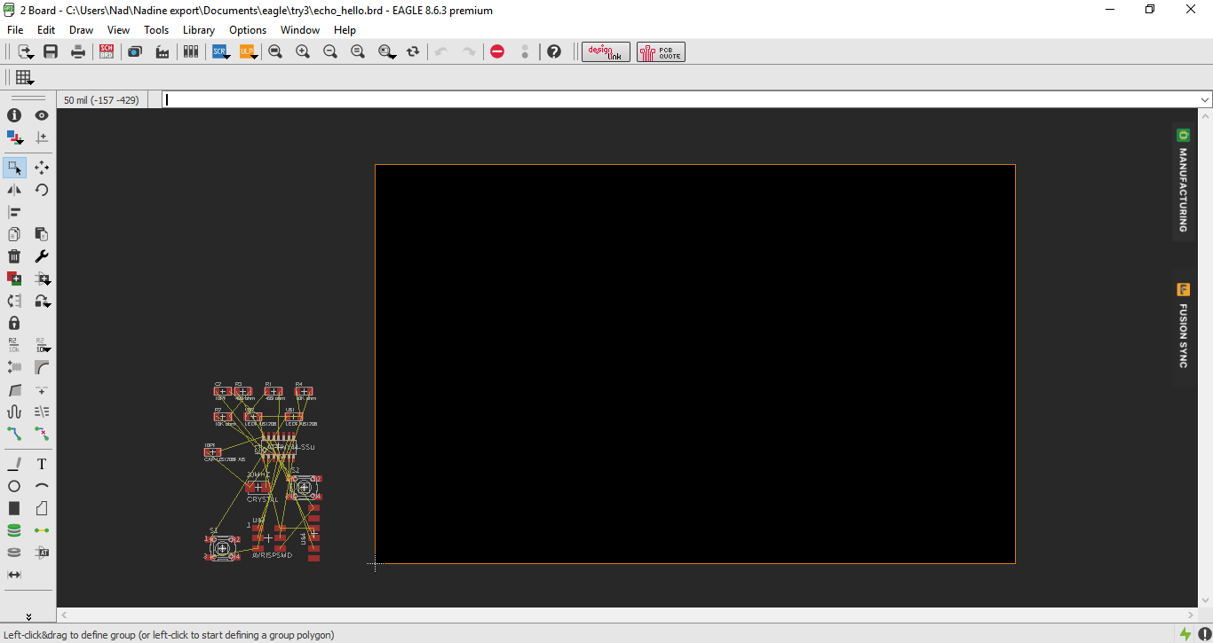
Select all the components and move them to the black area.
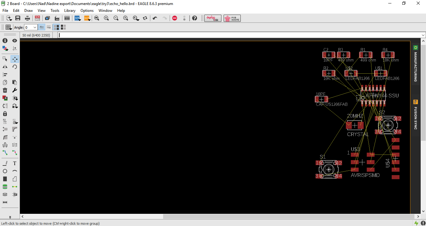
After that, you have to start changing the position and orientation of the components to find the easiest way to route them.
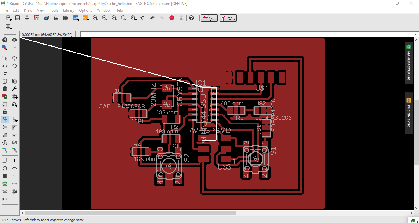
I started with the Attiny44 and the Crystal. Then I pressed ratsnest. What ratsnest does is that it shortens the connections between the components for easy routing.
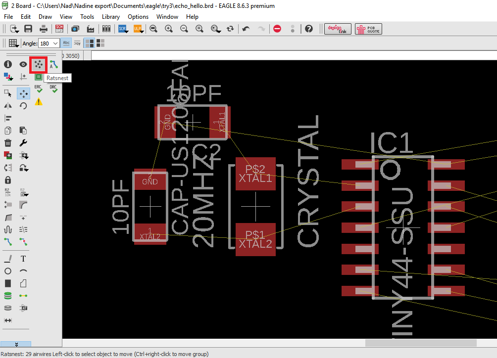
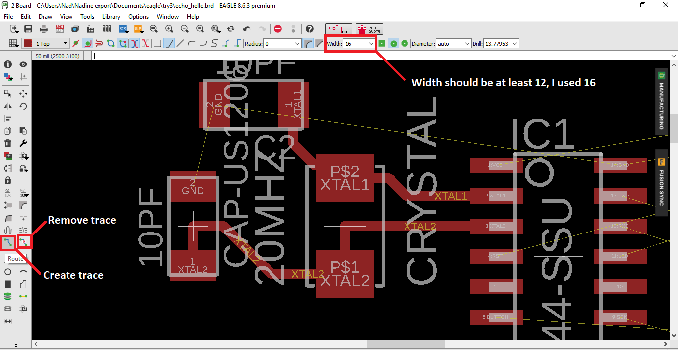
Then I started routing between the components using route and rip-route. I made sure the width of the trace is set to 16 to make sure my drillbit can drill it.
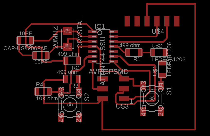
I repeated the same steps for all the components, leaving the GND connections till the end. My board looks like this now.
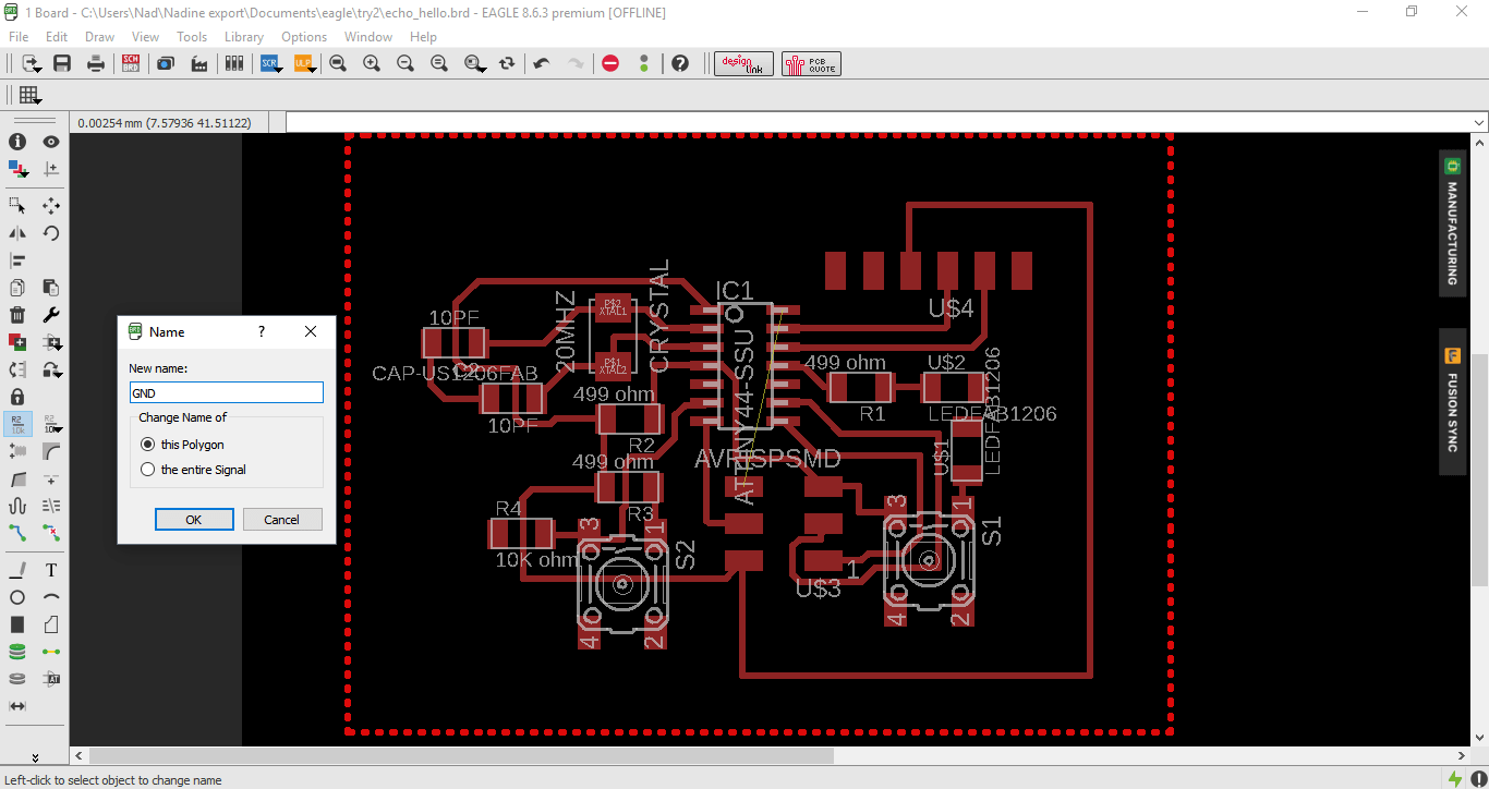
Next I drew a ploygon around my board and named that trace GND to create a common ground.I then pressed ratsnest to connect the grounds together.
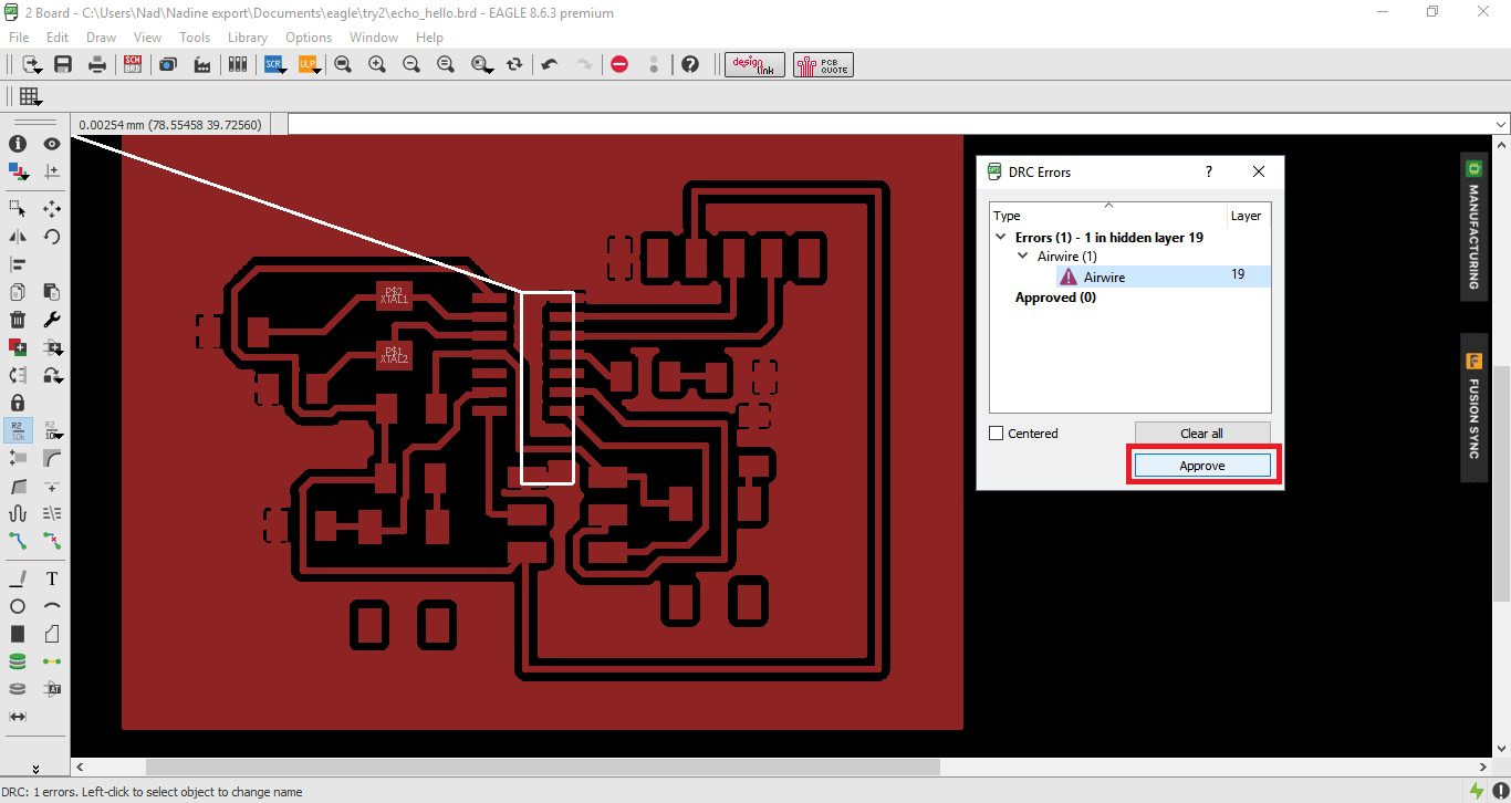
I don't know if you have noticed, but there's a single GND trace that I can't seem to route so I decided to do a little trick which is use a Zero Ohm resistor and let it jump pver the trace just to connect the grounds together.
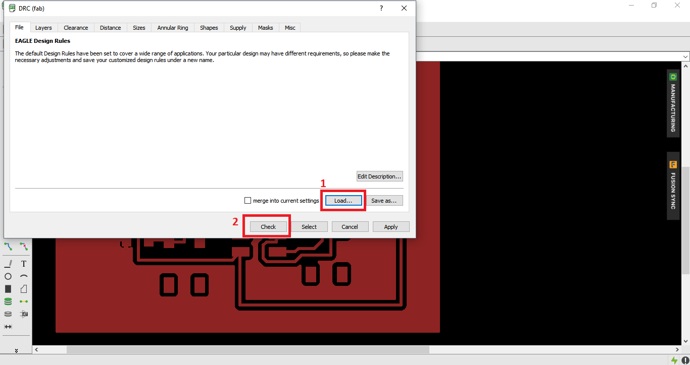
Design Rules Check (DRC) checks the board against a set of rules to make sure the board meets those rules. The rules are set for:
- layers: defines which signal layers the board actually uses.
- Clearance: defines the various minimum clearance values between objects in signal layers.
- Distance: defines the minimum distance between objects in signal layers and the board dimensions, as well as that between any two drill holes.
- Sizes: defines the minimum width of any objects in signal layers and the minimum drill diameter.
- Restring: defines the width of the copper ring that has to remain after the pad or via has been drilled.
- Shapes: defines the actual shapes for smds and pads.
- Supply: defines the dimensions of Thermal and Annulus symbols used in supply layers.
- Masks: defines the dimensions of solder stop and cream masks. We won't be using this.
- Misc: allows you to turn on a grid and angle check.
To make sure my design is free of errors, I downloaded the fab design rules and checked my design against them. The only thing that showed up was the GND that wasn't connected so I approved it since I'll be solving that with a zero ohm resistor.
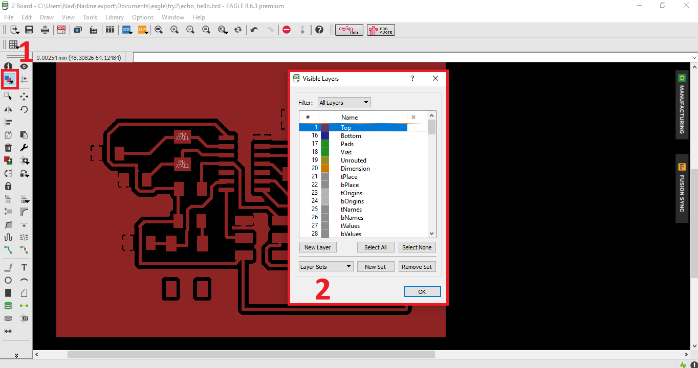
Then I exported my design as an image but after displaying only the top layer.
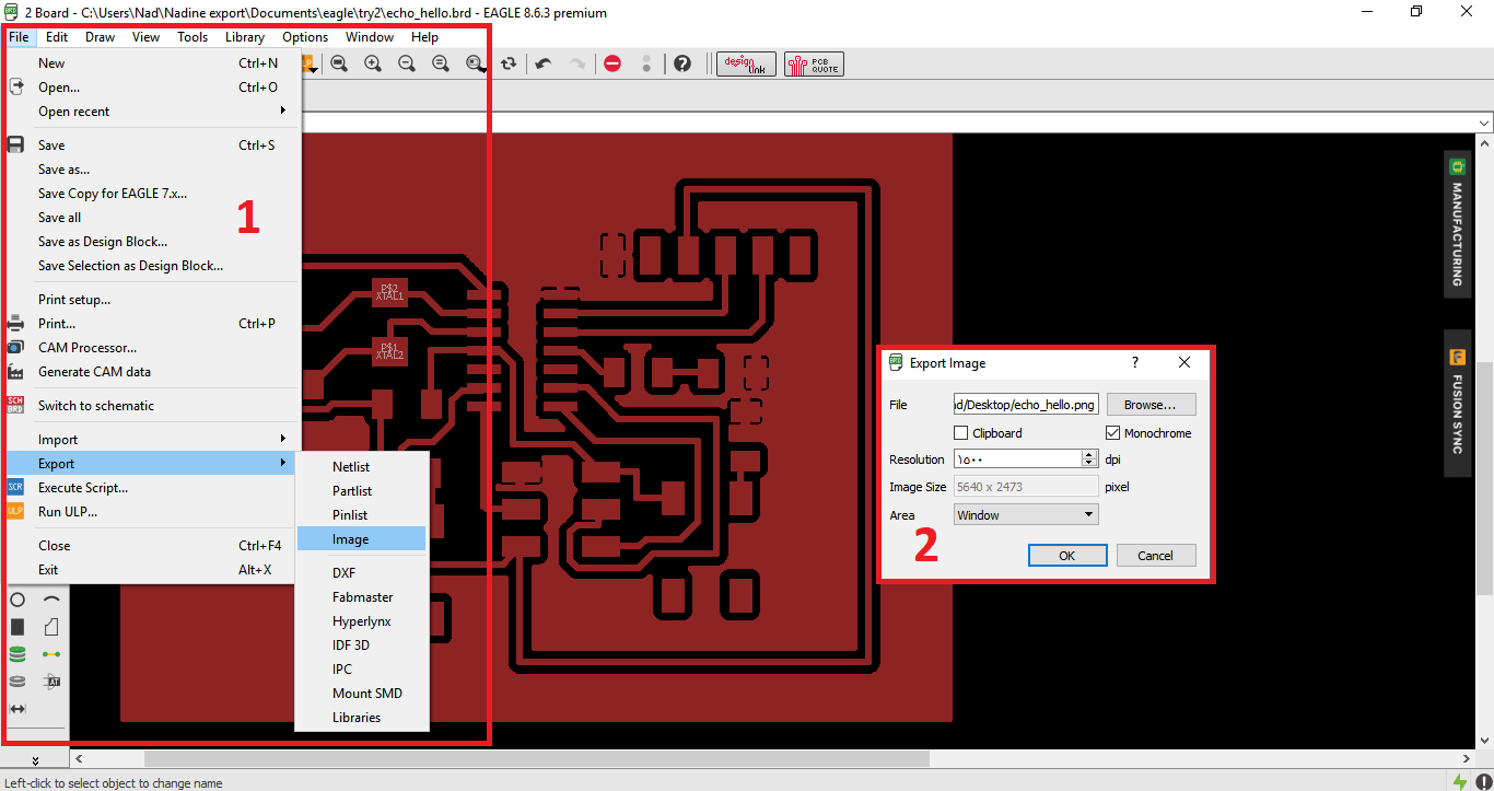
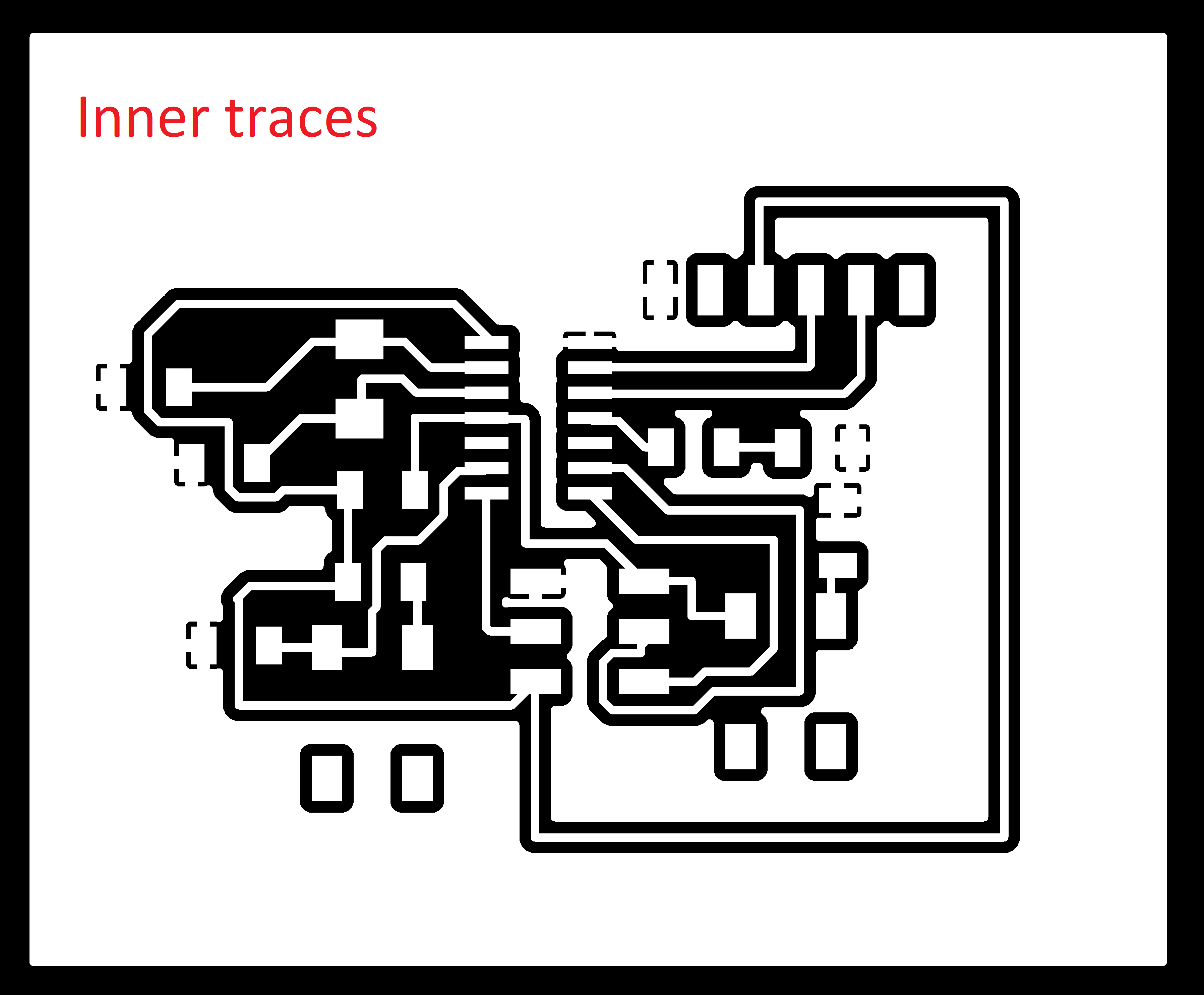
Then I edited the exported image to have the inner traces cut and the outer traces cut.
Making the PCB
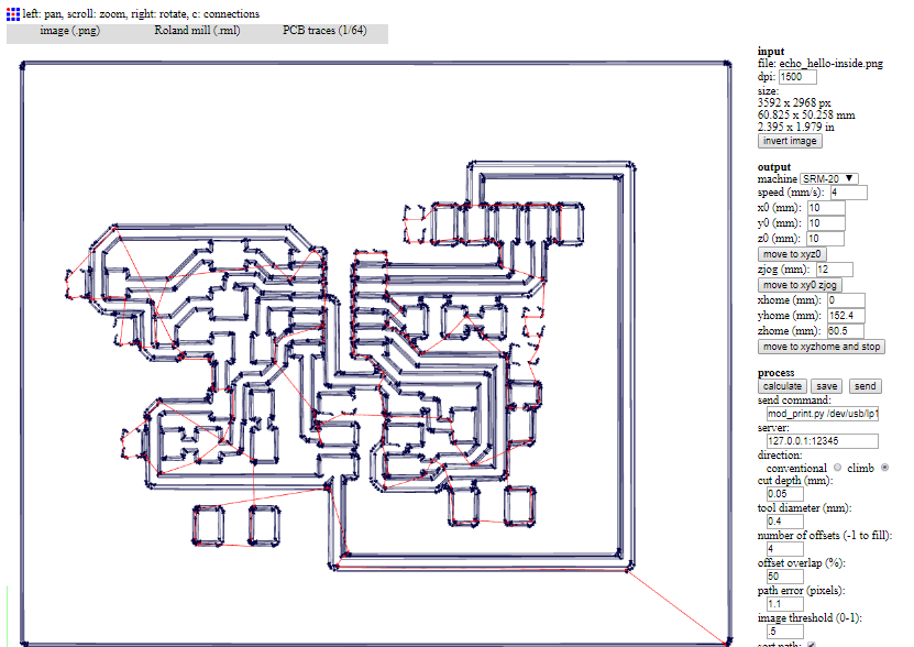
After that I inserted the images to the Fab Modules set the settings for the engraving process as seen below.
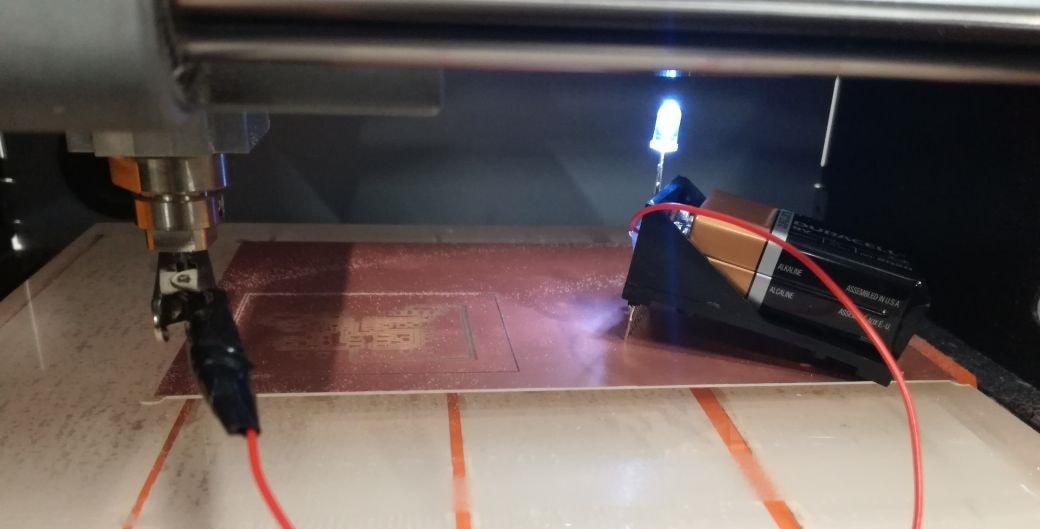
Then I calibrated the Roland SRM-20, chose the X & Y and the zero for the Z.
To calibrate the Z-axis, I used a tool that the electronics engineer, Osama built. A clip is connected to the endmill and the battery is placed on the copper sheet, if the endmill touches the copper sheet a light will light up.
The cut board had some miss alignments and some traces weren't milled correctly so I cropped the inner traces image to have only the traces that weren't milled and launched another milling job.
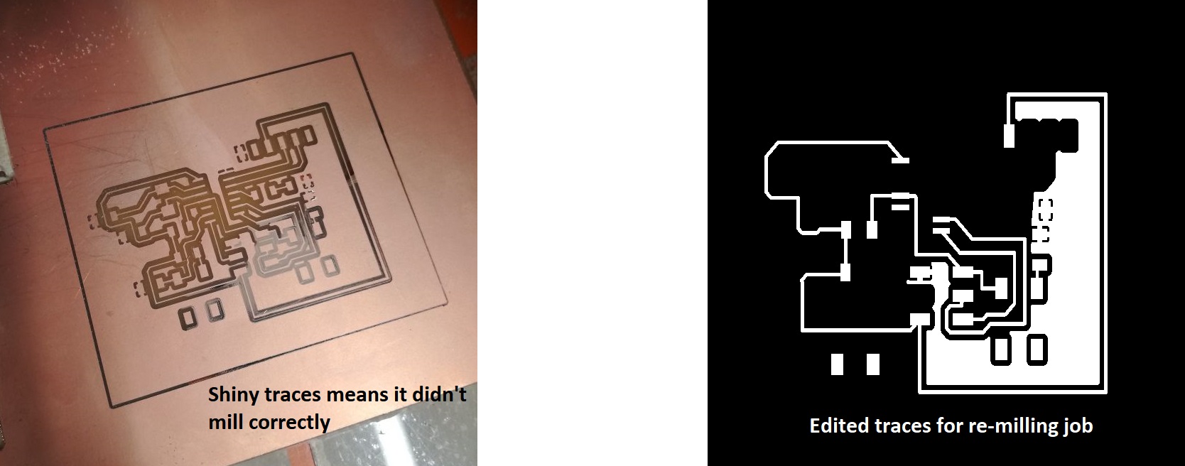
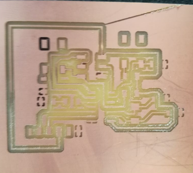
I guess that day just wasn't my luck day cause the re-milling did fix the miss milled traces but it also chopped off other traces :(
So I decided to re-mill the entire board!
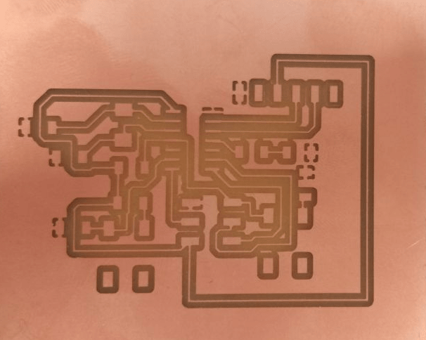
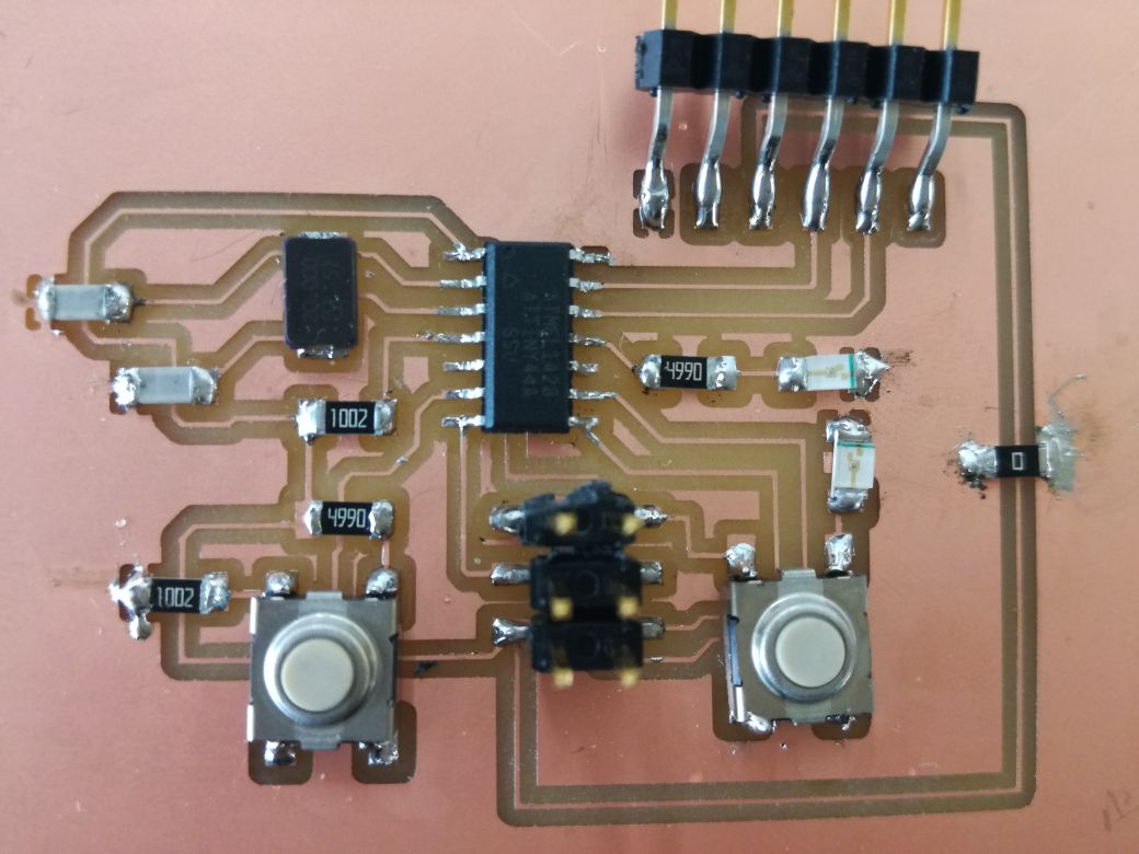
The second board I milled turned out perfectly! Yaaaay!
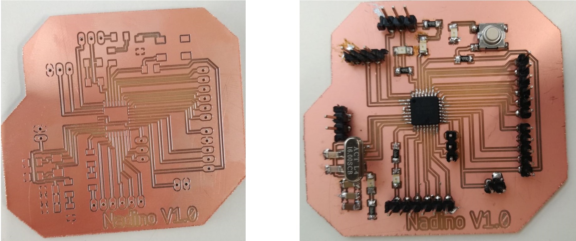
Next, is the other hard part! Soldering. I displayed the tplace layer and the name layer in Eagle to guide me through the soldering process. Imagine misplacing components after all the hassle I went through!
And here's my finished board! Isn't it just beautiful?
Programming the Echo Hello
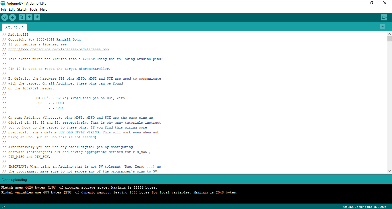
Another tricky thing we had to do this week is to program the board. I chose to program it using the Arduino as an ISP.
The first thing I did was patch the arduino to recognize the Atmel Attiny44 microcontroller we used.
To do that I followed the steps in this tutorial.
Then I connected my Arduino and uploaded the Arduino ISP program from examples on it.
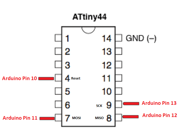
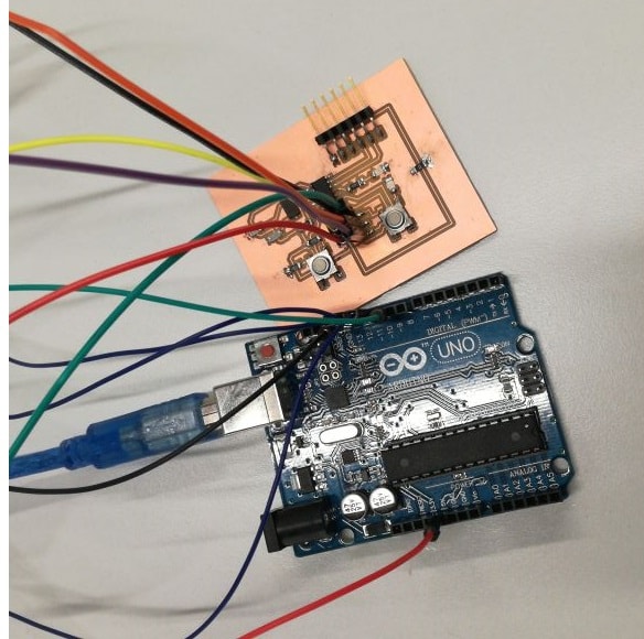
After that I connected my PCB to the Arduino using the same connection we made before in Electronics Production Week and as seen below.
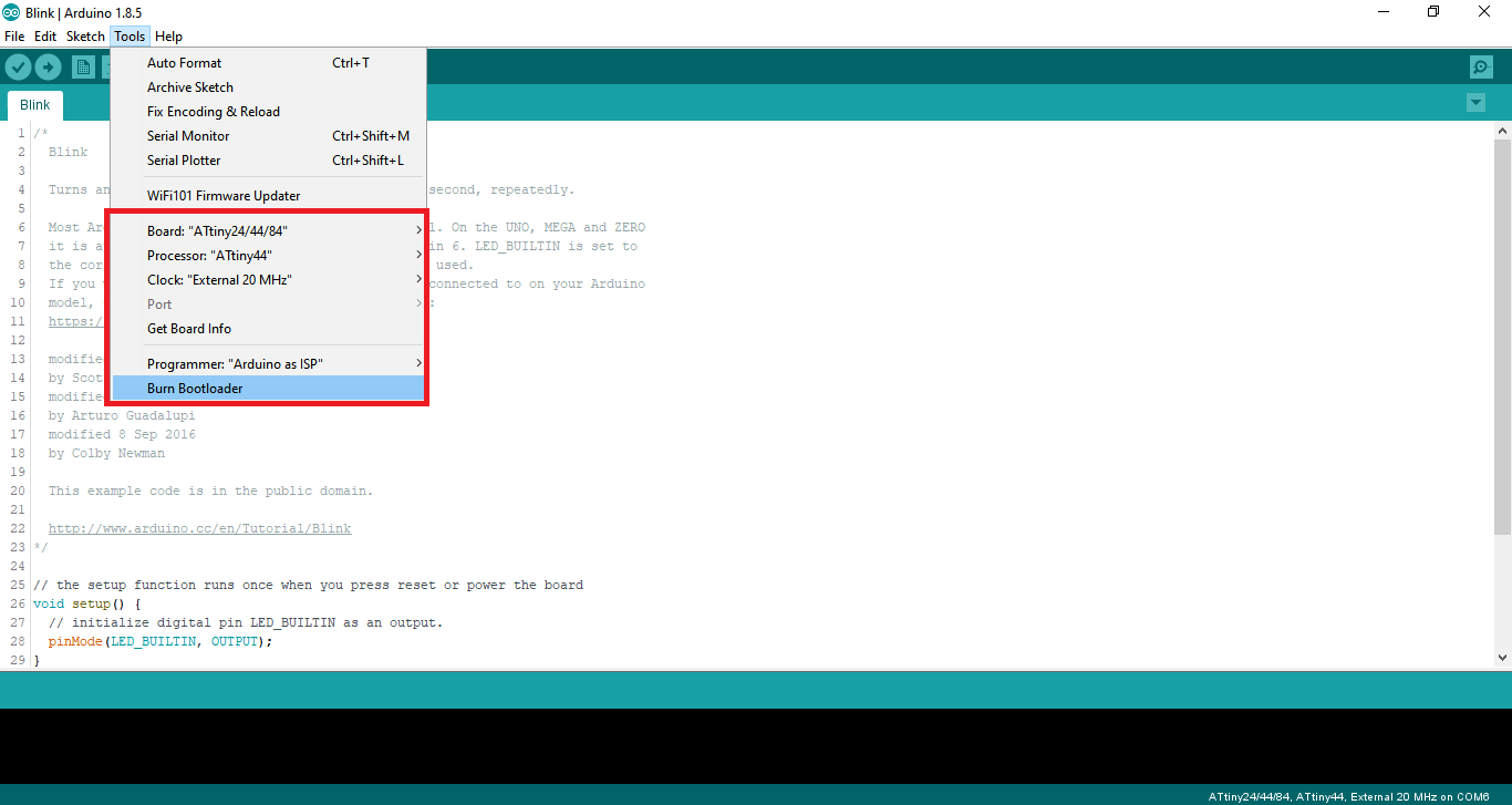
After that I choose the following to burn the bootloader:
- Board: Attiny24/44/84
- Processor: Attiny44
- Clock: External 20 MHz
- Programmer: Arduino as ISP
Then I pressed burn bootloader. It should display done and it did!
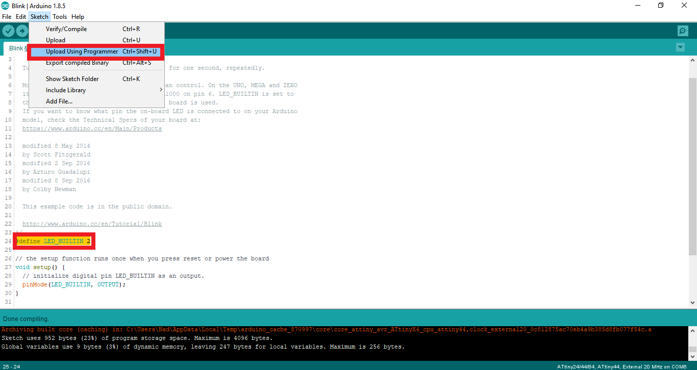
Next I wanted to make sure I could program it, so I chose to upload the blink example but after modyifying the pin to 2. At first I thought my board was fried because I was using pin 11, but after going back to the datasheet it was actually arduino pin 2 *phew*.
To upload it you should use upload using programmer instead of upload.
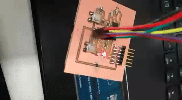
And guess what happened, my board started beating *tears of joy*
The making of Nadino V1.0
Our instructor Dima really wanted us to practice our PCB Design skills more, so he pushed us to make our own Arduino Board.
Following Daniele Ingrassia's Satshakit which is an improved and fabbable , 100% Arduino IDE/libraries compatible board.
I decided to call mine the Nadino. So I first started with the schematics. The arduino uses the Atmega328P. So we first downloaded the library of the component for eagle.
Then I started connecting the pins of the microcontroller to labels as seen below.
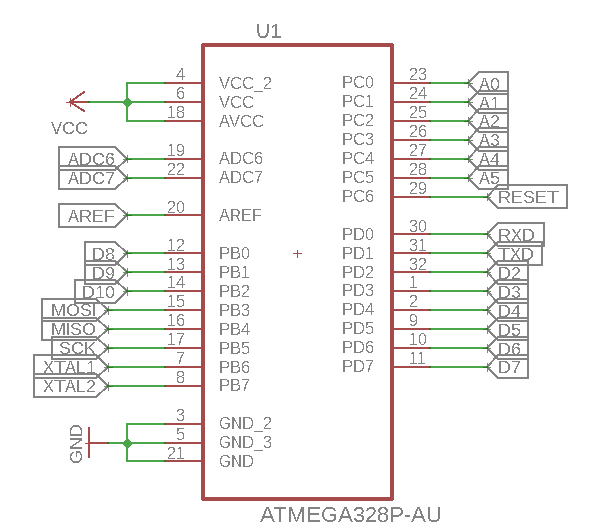
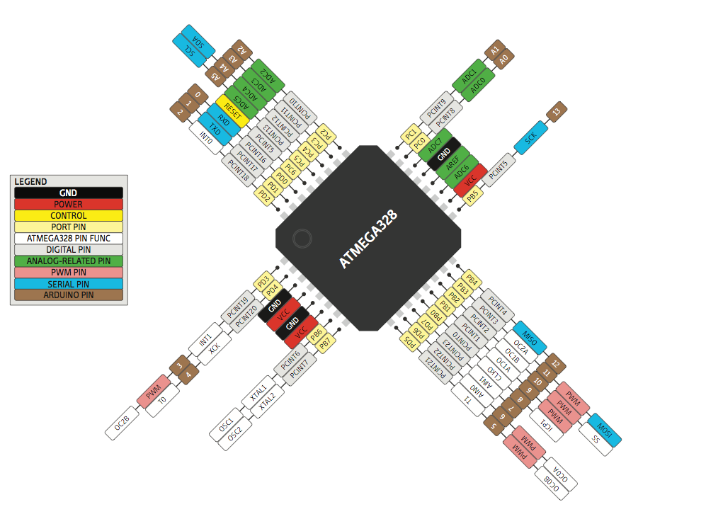
To connect the labels correctly, I refrenced the below seen pinout.
When I made the echo hello board, I had a bit of trouble connecting all the components at the same time when I started designing the board. So this time I connected a component in the schematics and then immediately switched to board design and connected it there as well.
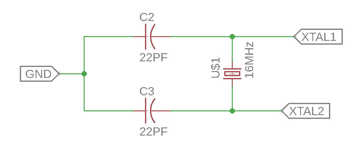
I first started with the Crystal. The crystal I used is the 16MHz although the Atmega 328P can run on up to 20MHz. The recommended capacitance to use is 22PF. The circuit for the Crystal is seen below.
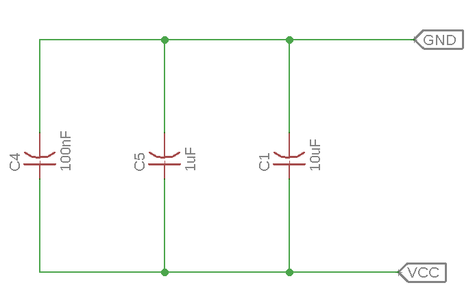
Then I connected other capacitors with values of (100nF, 10uF & 1uF) in parallel and connected to the VCC and the GND. The goal of this circiut is to make the board more stable.
After that, and going back to the pinout, I chose which pins should be connected to pin headers. I chose pins in a way that made connecting them easier while I'm designing the board.
I connected the pins to pin headers as seen below.
As you can see, I decided to connect some LEDs to certain pins for example to the RXD and TXD. This way the LED will light up when a signal is sent to the RXD or the TXD pins.
I also added a reset button and an LED connected to it, the LED lights up when the reset button is pressed.
I also added an LED that lights up when the board is powered.
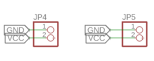
I have a couple of pin headers that are connected to GND and VCC. I added those cause usually we need more than one VCC pin and one GND pin.
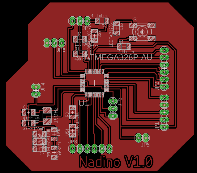
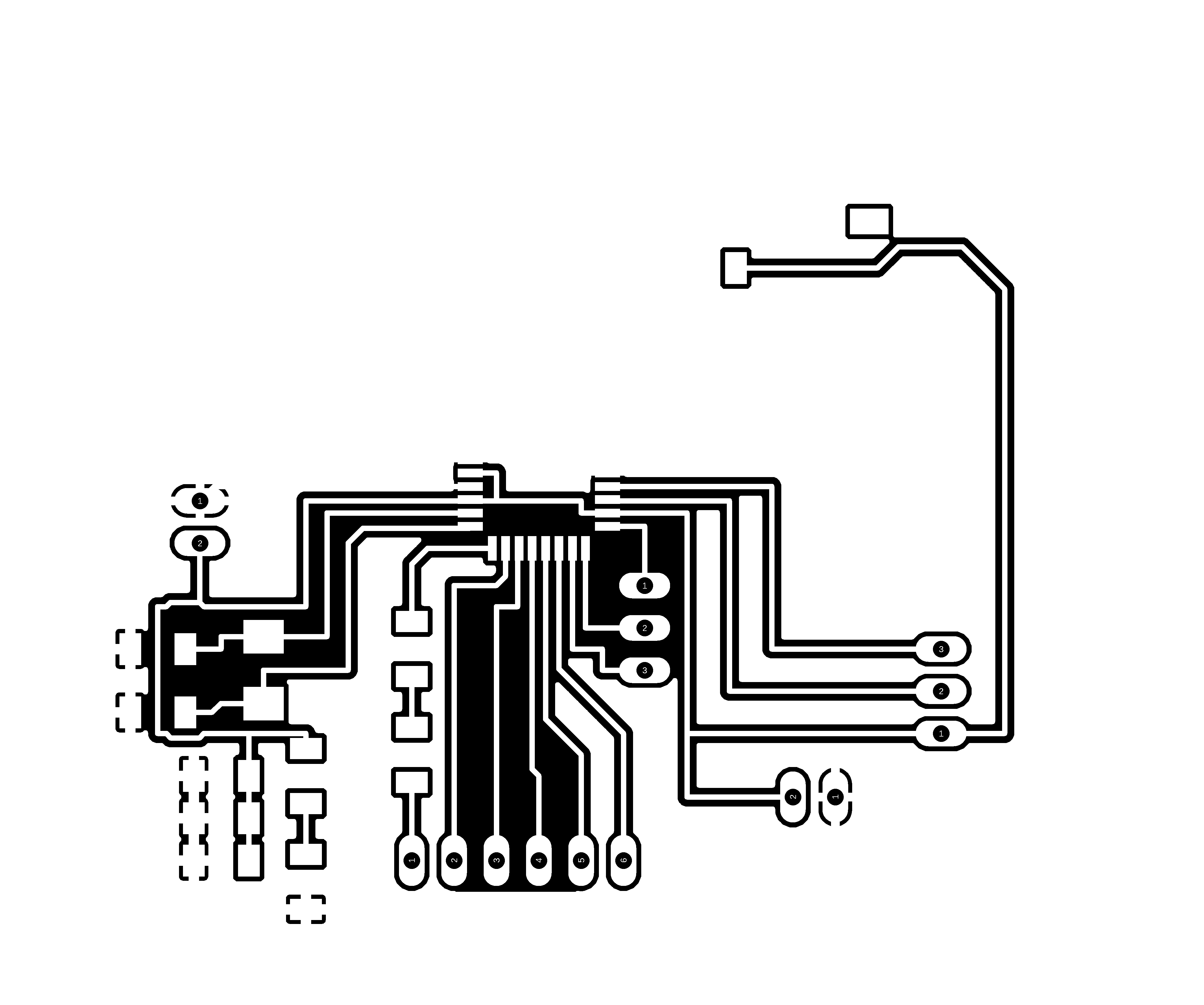
The finished designed board looks like this. The milling process will not be easy that's for sure!
Milling the Nadino V1.0
To start the milling process, I exported my design as png. I made 2 exports, one for the traces and another displaying only the pads layer to the drilling for the pin headers.
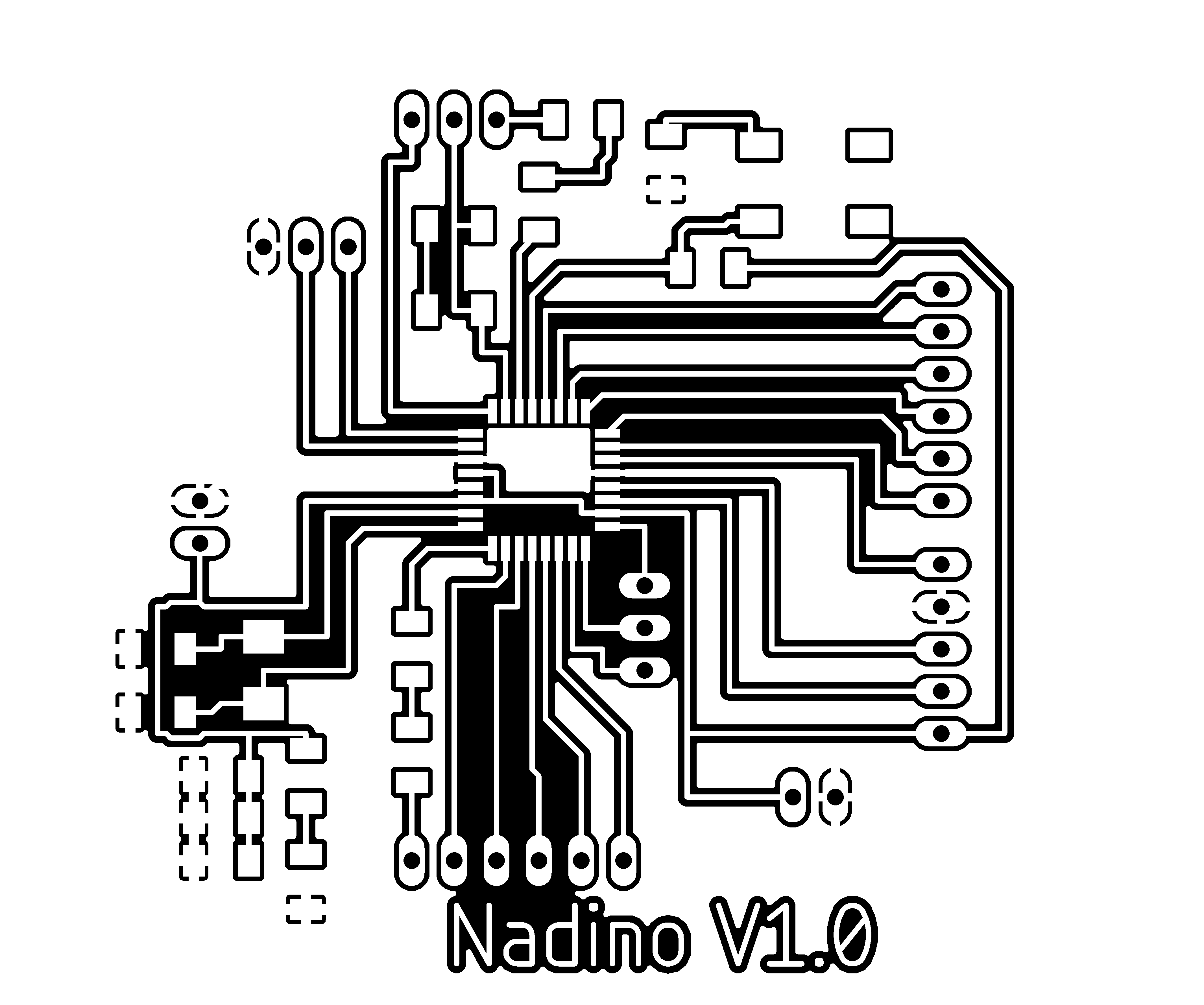
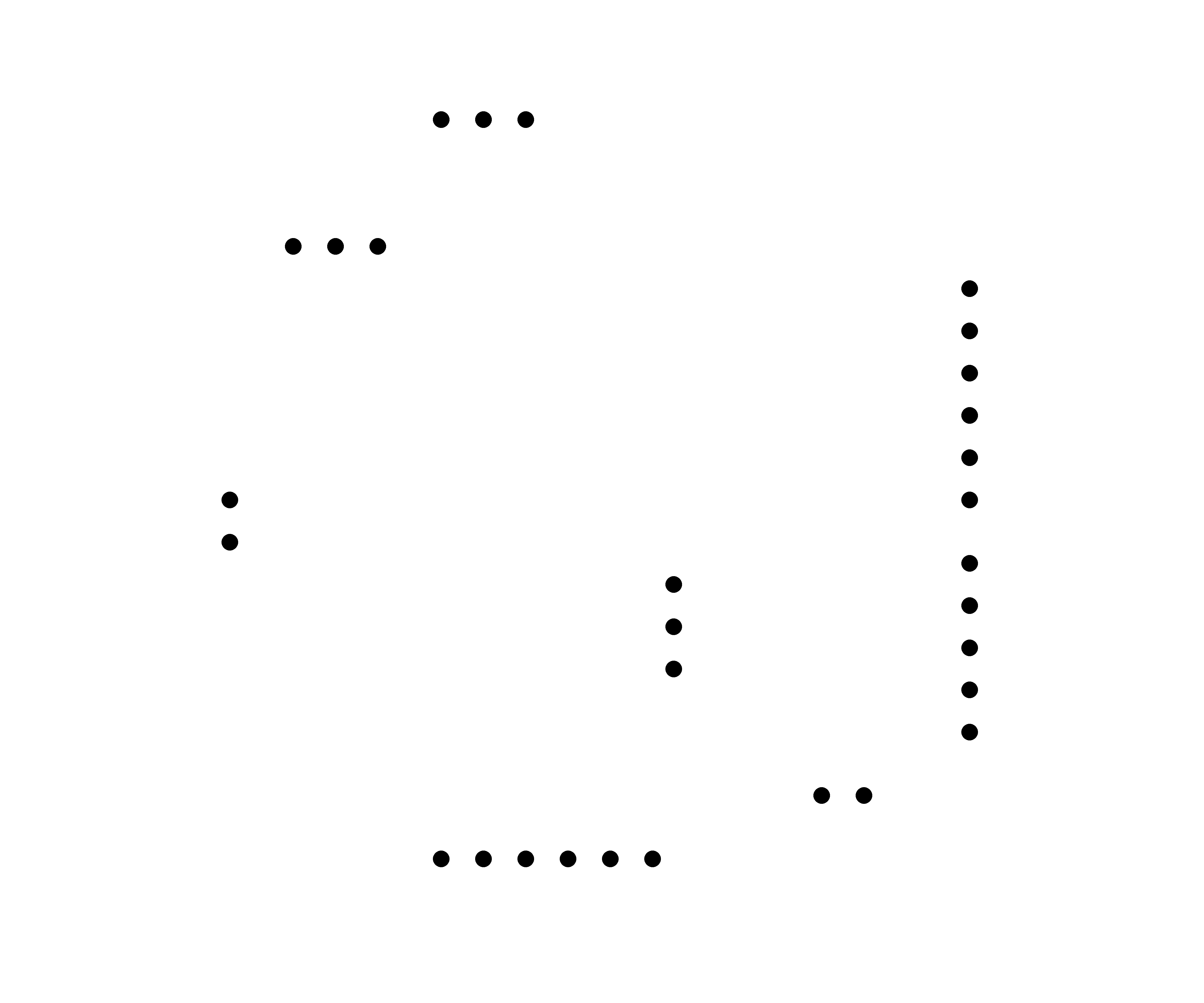
I had to edit the exported pads image to have only the drilling holes as seen below
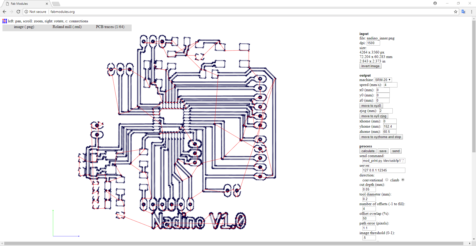
Next, I uploaded the inner traces image to the Fabmodules and set the settings as seen below. The end mill we used to mill this board is a 0.2mm drillbit.
The milling was kind of okay. Unfortunately there was a miss alignment so I croped the image to have the miss milled traces and re-milled them.
But it still didn't work :(
so I decided to go through with the drilling and fix the miss alignment by hand.
The settings for the drilling and cutting are seen below. Of course I changed the drillbit and choose a different zero for the Z-axis.
The finished board with the fixed miss alignment is seen below. Unfortunately I accidentally cut a VCC trace while I was fixing the miss alignment but I will fix it while I'm soldering.
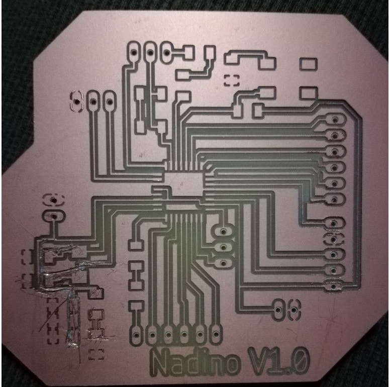
I tried to find a way to reconnect the traces that I accidentally cut, but it was too difficult, so instead I just milled my board again. Dima, our instructor, did surfacing on the Acrylic that holds the copper sheet to make sure there isn't any miss alignment. And My board came out perfectly.
You can download my designs here:
