Electronics Design.
Concept
The scope of this session is to reproduce the "Hello Board". That said implies creating the logical structure, or the schematic for the microcontroller(MCU), in our case Attiny44. Burn it's bootloader, meaning install the firmware upon which the MCU is going to execute the operations.
As mentioned in Electronics Production week, the software of choice is Eagle. This softwar is purposefully made to help throughout the schematic and board layout design process, as we will see in the upcoming session.
Attiny44 MCU.
Each MCU has it's own technical specifications and pinout scheme which can be found in the datasheets of the component. Attiny44's datasheet can be found here. Here we can mentione couple of useful information regardin the Attiny 44 MCU:
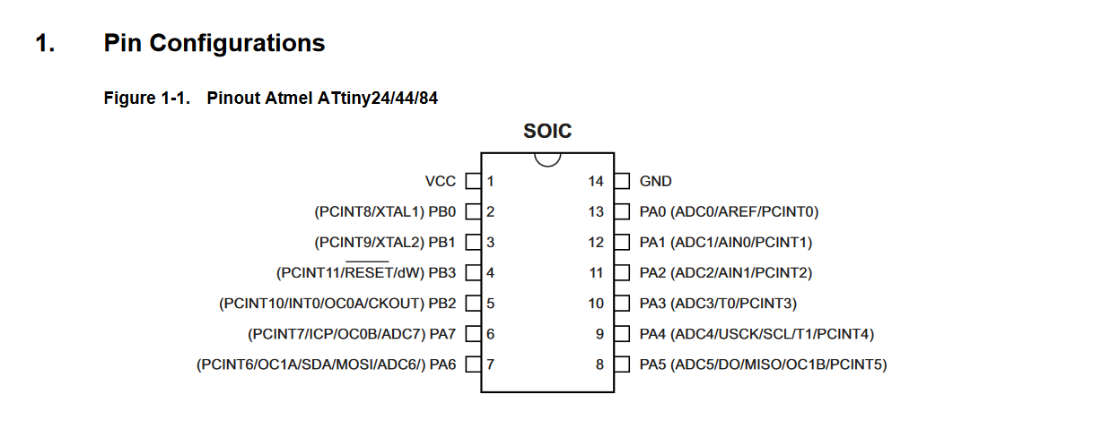
This is helpful during building the schematic, as it lays out the logical connections of the MCU.
Schematic Design.
In order to get started on some good components that we can add to our schamtic, it is important to download the Fab Library as it contains most important components that one can use during the simple board design process.
Here is an example of importing the "Fab_Hello" library:
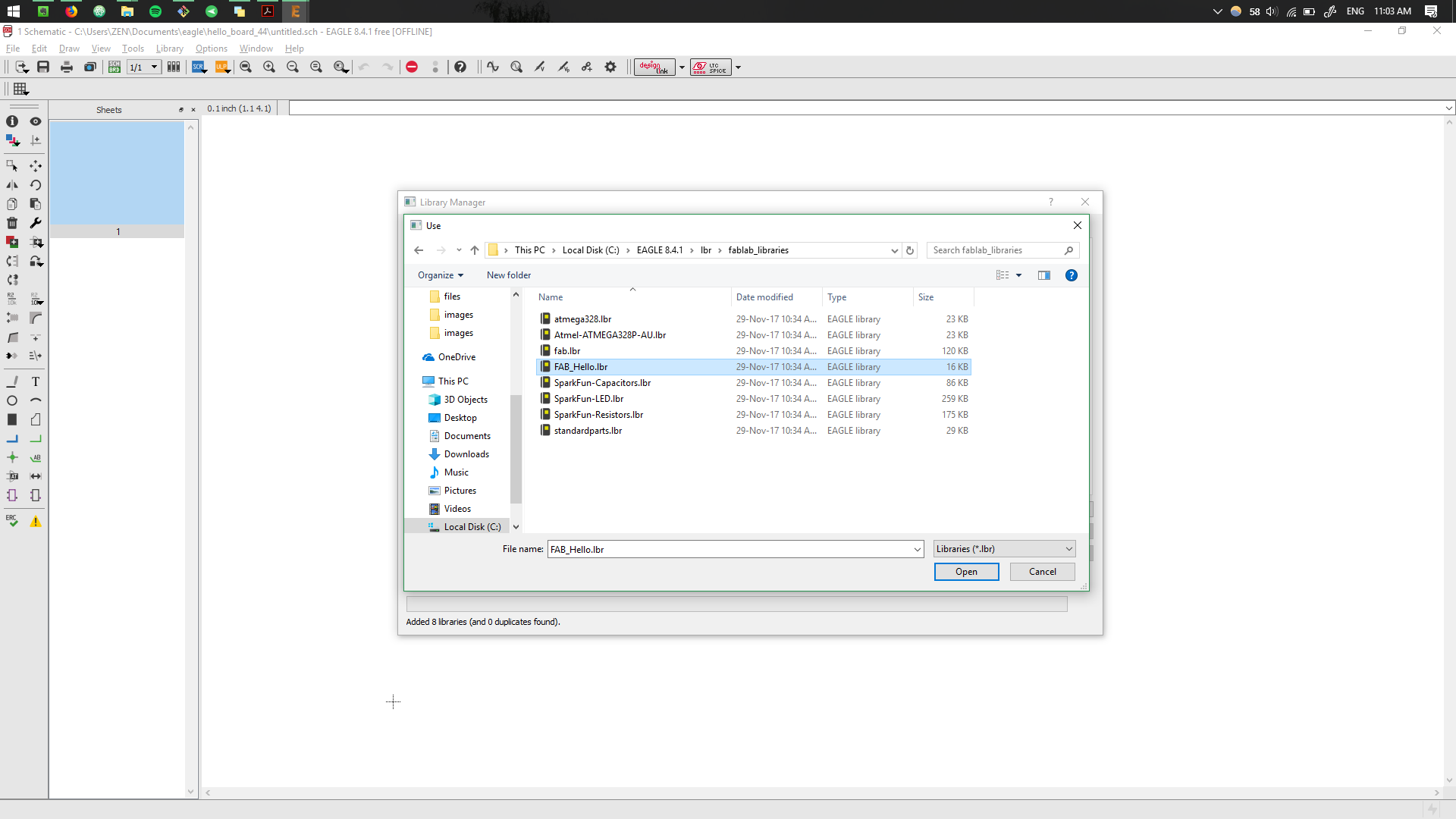
To add the library to the software, one can access the "Library Manager" and indicate the downloaded library.
To start adding components to the schematic, it is enough to type
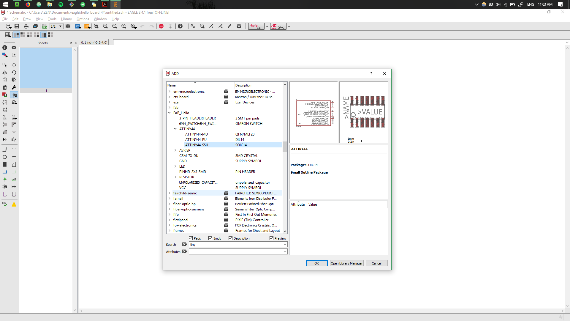
Once the component is found, we can then place it into our circuit sheet.
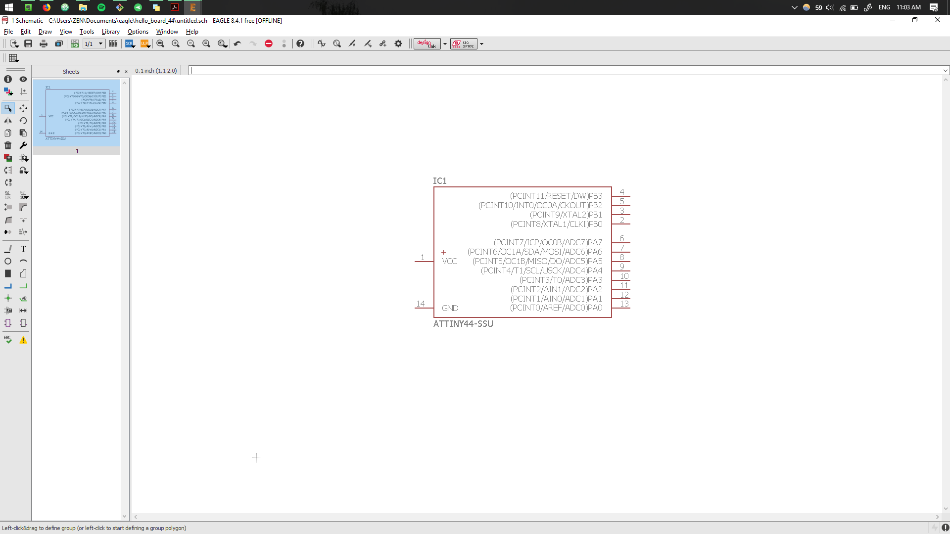
This is a simplified representation of the controlling unit, which allows us to connect the pins to other components and power supplies.
SPI.
In order to give life to the MCU the bootloader needs to be executed. The interface to accomplish that is Serial Periheral Interface Bus(SPI). This same interface is used to program the MCU.
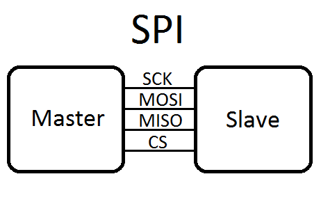
The way the SPI interface is wired between the "Master" and the "Slave" device.
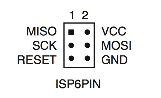
Nice way to concentrate all the pinouts of the SPI interface, including VCC and GND for power.
UART.
Another interface is Universal asynchrnous receiver-transmitter(UART). Using this interface we can directly communicate through transmit pin(TX) and read pin(RX) with the board at different baud rates that the MCU allows.
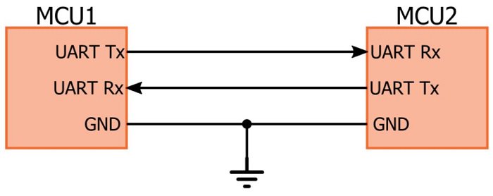
The way the UART interface is wired between two MCUs.
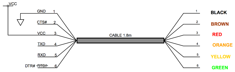
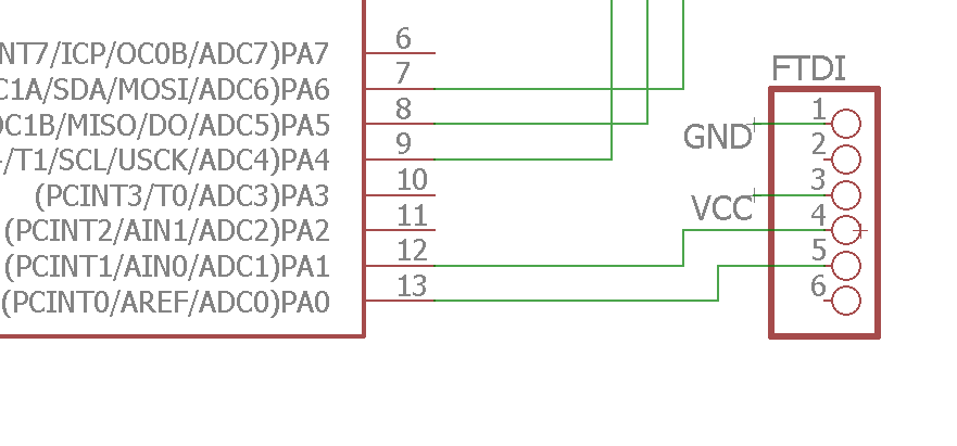
FTDI cable that allows the communication. It uses six pins, out of which only four are necessary to accomplish the job.
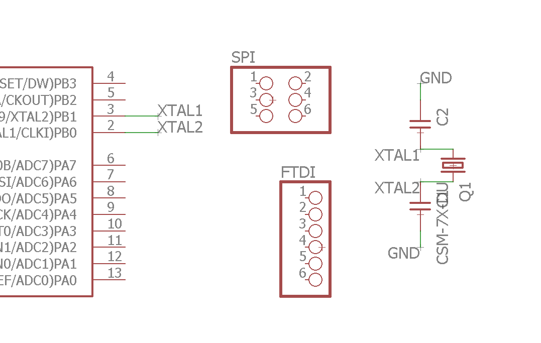
Clock.
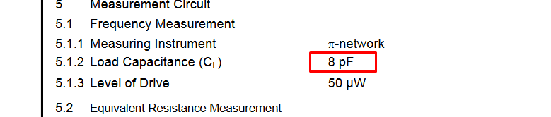
To extend the speed of the MCU, an external clock can be added. The internal operational speed of the Attiny44 MCU can get up to 8 MHz. Thus by adding a 20 Mhz external clock we extend the speed by 2.5 times.
Usually it may require some capacitance to make it operate. This can be found in the datasheet of the crystal. It is suggested to use a 8pF capacitor.
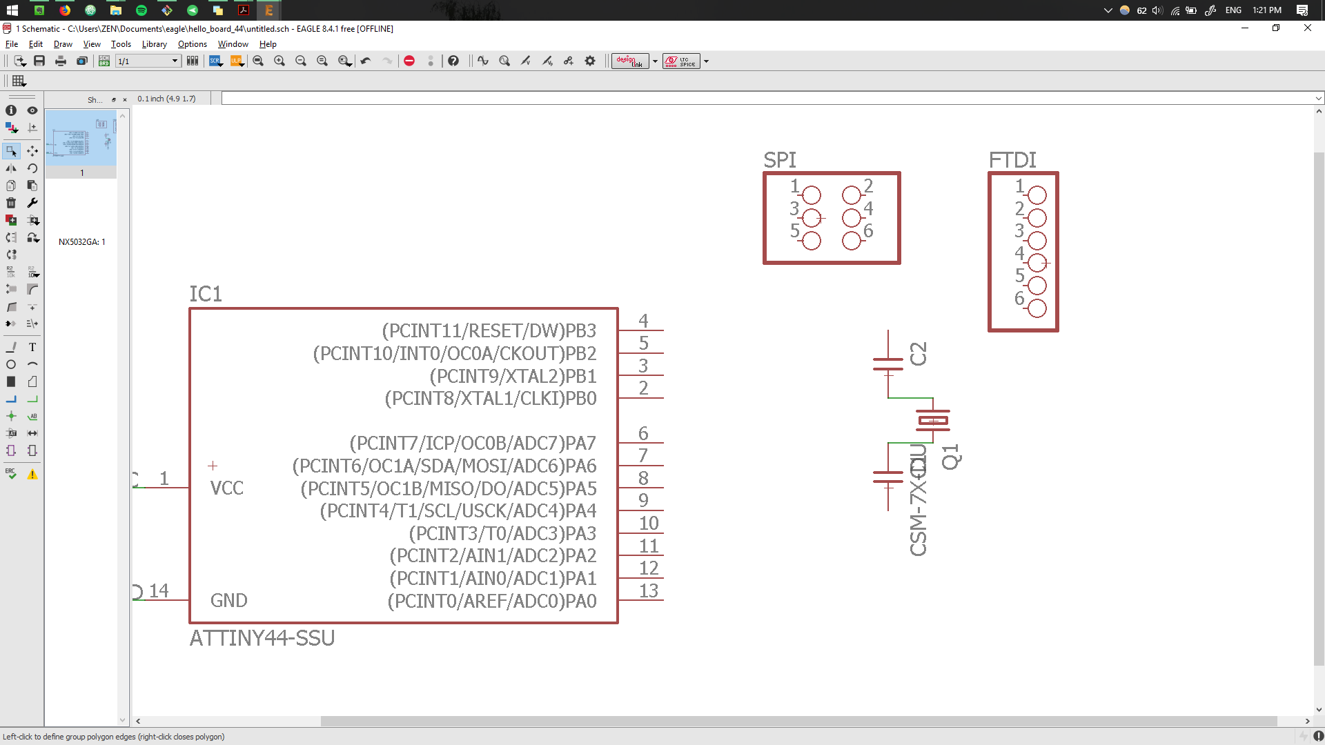
To add the SPI pinouts, UART pinout, crystal clock and necessary capacitance, all can be found a the fab library.
Logical Connection.
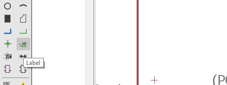
In order to start logically connecting the components, one can instead of wiring, a function called labeling the traces.
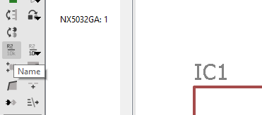
First the label is placed.
After which it is named.
As a result we connect the pins of the crystal clock to the MCU, using
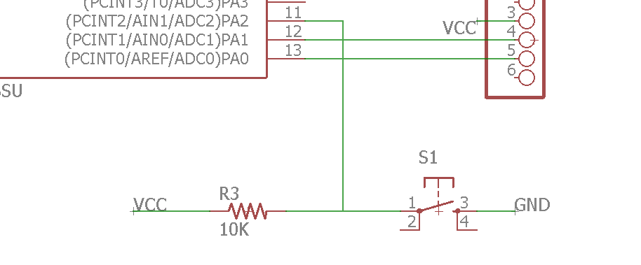
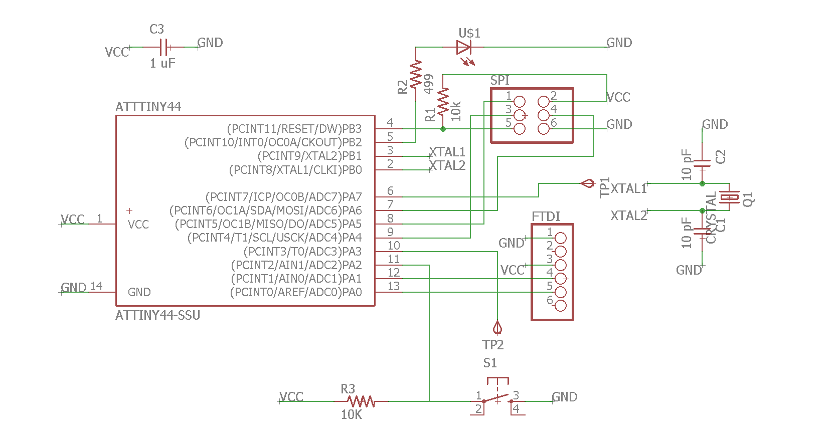
This is the connection of the SPI interface to the MCU. The 10k resistor connected to the VCC allows the MCU to Reset. While the use of the LED connected to the PB2 will allow later to use this as an

In a similar fashion the UART interface is wired to the board, using
To introduce an
Finally, to avoid any noise interferences, an addition of 1uF capacitor is added between the VCC and GND.

Circuit schematic is ready. This means we can proceed to creating the board layout.
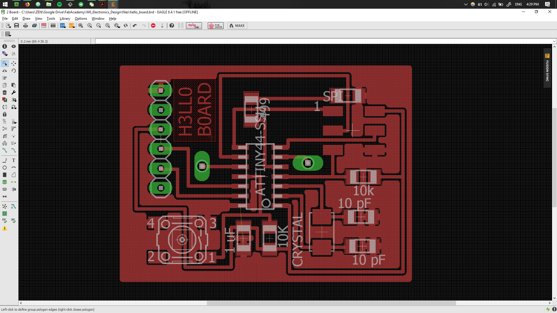
Board Layout Design.
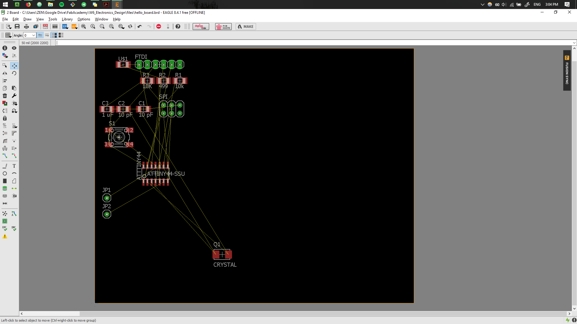
We enter into the board editing environment. At first the components are randomly placed. However the goal is to untangle this mes of yellow line connections and rearrange the components in such a fashion that the MCU is located in the middle, while the rest of the components are situated arround.
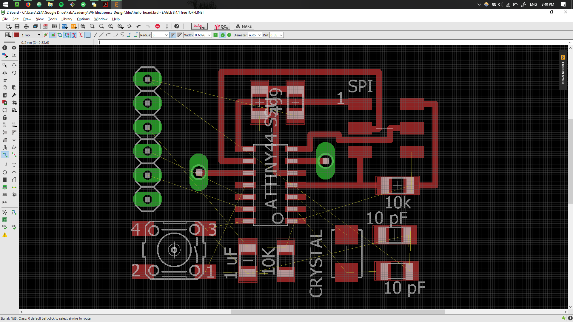
By using the
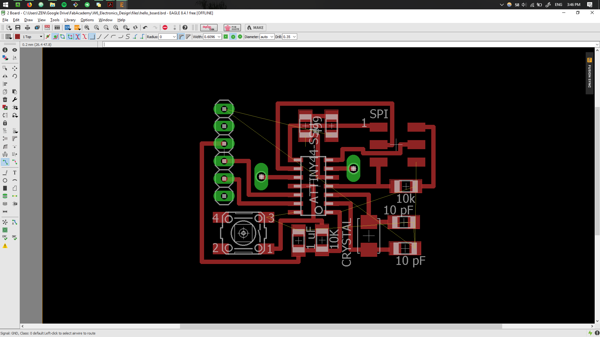
As a result all the components are connected. I left the
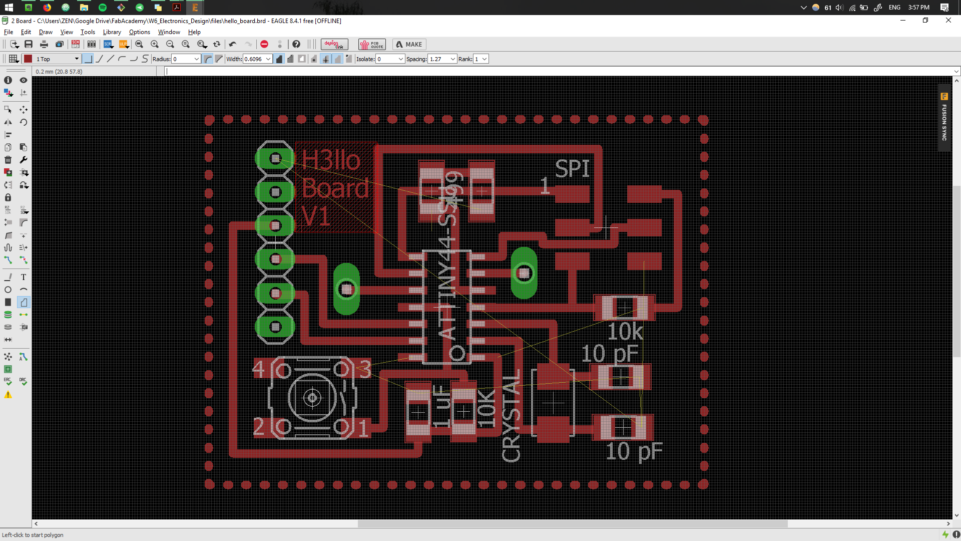
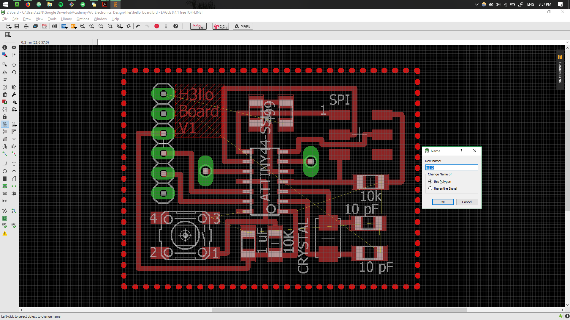
A polygon is created around the components. If connected properly this will result in dotted line around the perimeter.
Using the
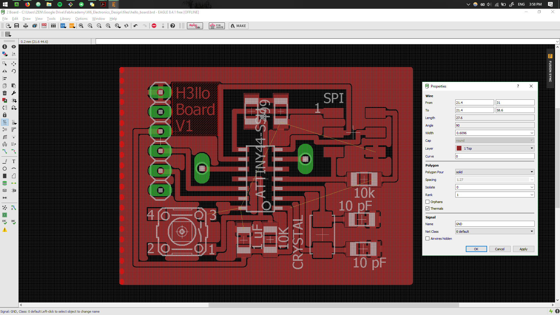
In order to adjust for the spacing between the cover area and the paths, by second-clicking on the polygon we can indicate the
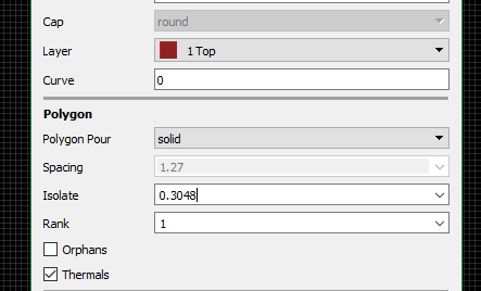
Here the value is increased, thus making it 0.3 mm away from the pads.
This results in having the entire polygon filled with TOP layer and the pads which reference GND are connected to it.
Creating the gcode files.
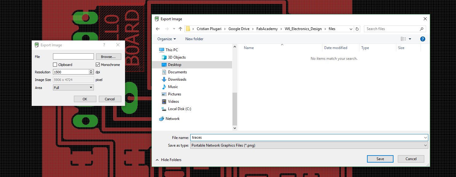
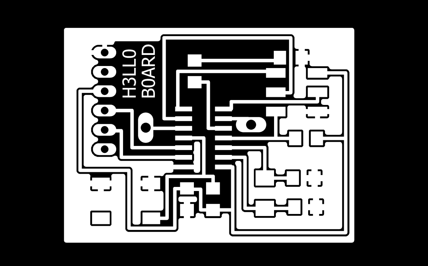
To send this job to the Milling process, we first need to export the image.
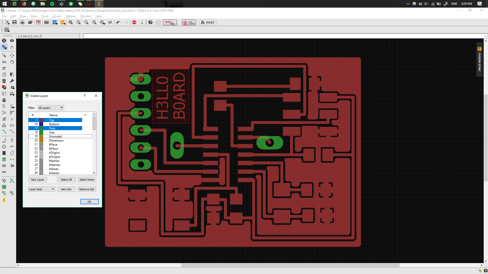
Before exporting it is important to select the necessary layers that we want to export. Usually it is
By going to
Once exported, we generate the monochrome image in order to create the gcode for the CNC machine.
It's time to use FabModules in order to generate the gcode files for the Roland Machine. Detailed approach is discussed in the Electronics Production session.
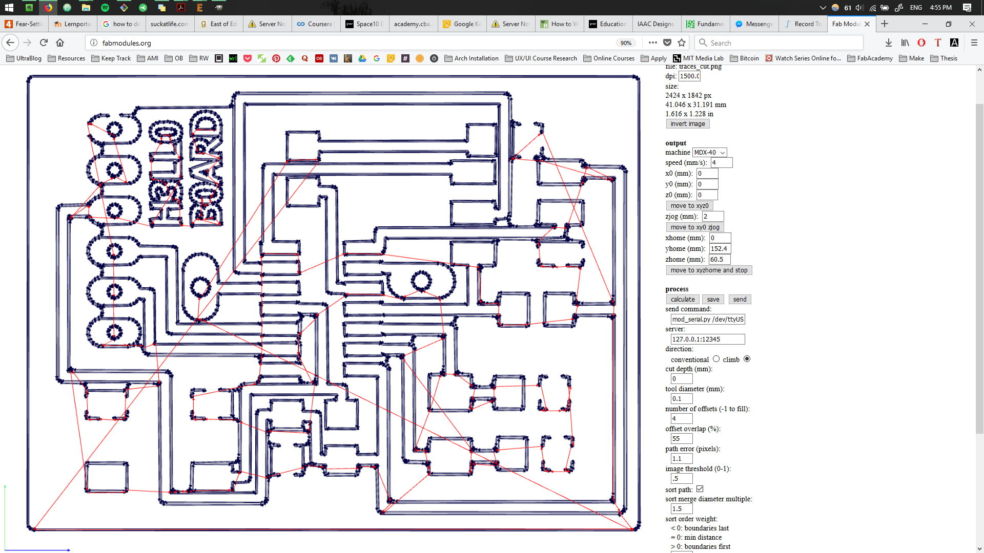
The settings used:
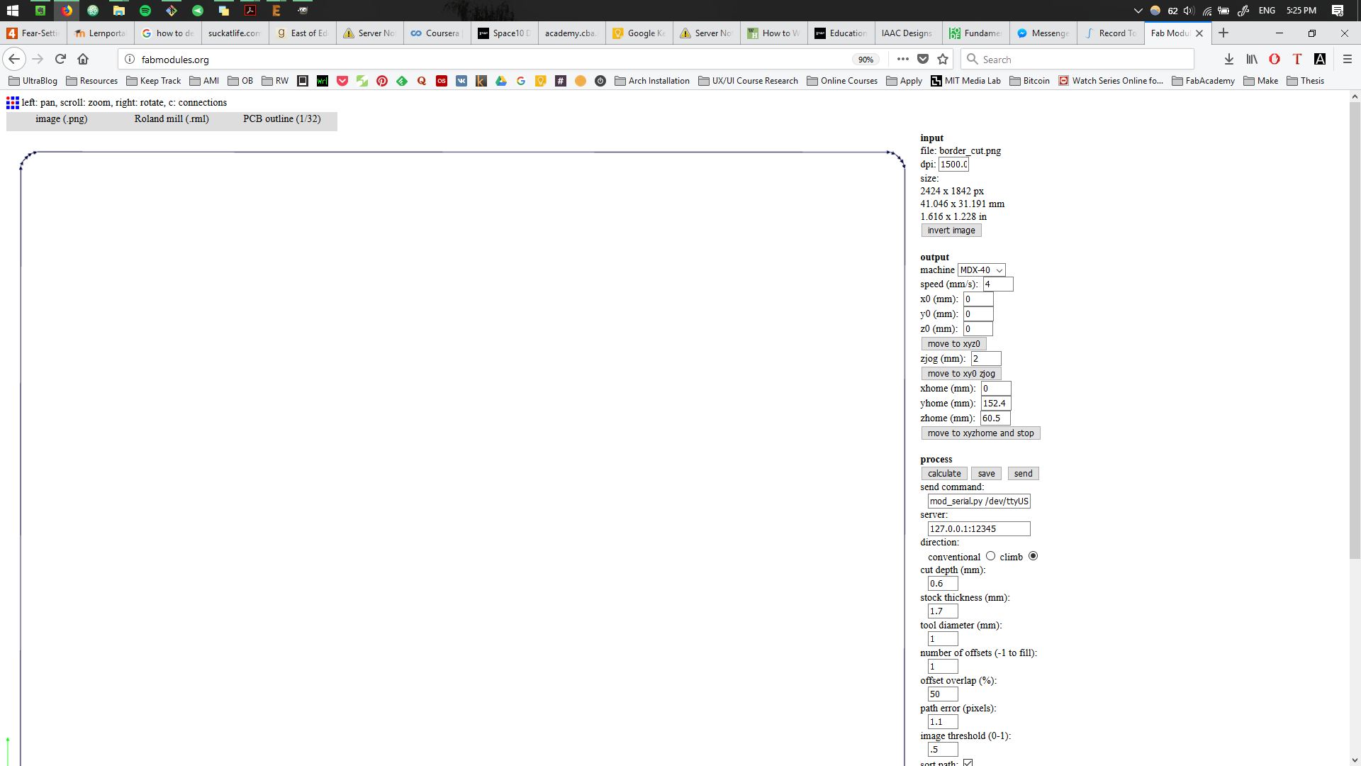
The settings used:
Milling the Board.
Details of how to mill the board properly is discussed in Electronics Production session.
.jpg)
A tool of 0.10 - 0.15 is used for the milling.
.jpg)
Pausing the job to see if the process looks good.
.jpg)
.jpg)
.jpg)
Cutout with the 1mm tool.
.jpg)
Board looks perfectly milled.
Soldering the Components.
Details of how to solder the board properly is discussed in Electronics Production session.
.jpg)
Component list.
.jpg)
Soldering the chip.
Final result.
.jpg)
Testing.
To give life to our board, it is crytical to install the bootloader. Here the FabISP board will be used, previously created in Electronics Productionweek. We connect the FabISP to our Hello Board by means of SPI, avoiding the 5V connection. For that the FTDI cable will come in handy, which is connected to the other UART interface.
To "burn the fuses" or bootload the board, one needs to download the firmware.zip and extract it somewhere in the PC.
To accomplish the programming one can follow either the tutorial here or the description below.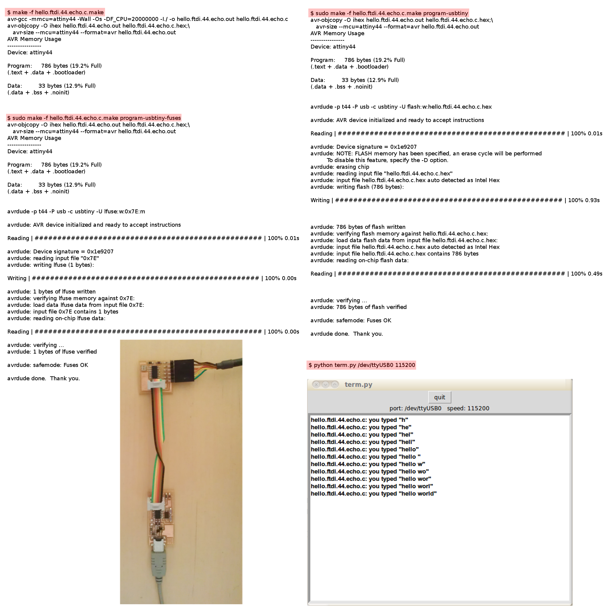
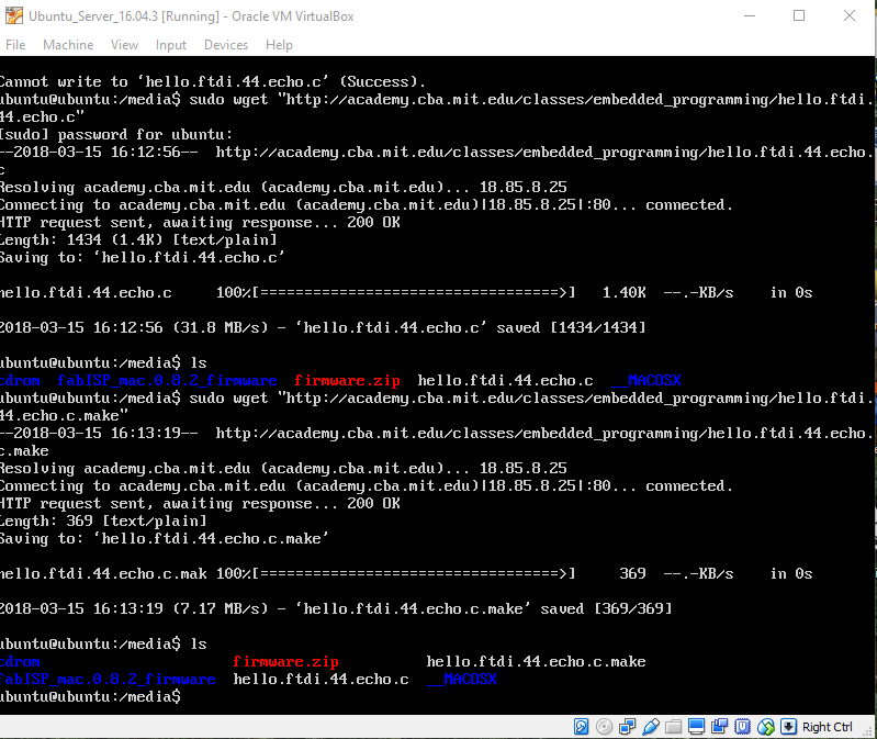
Once the firmware is extracted, we need to modify in the main file the version of the MCU from
sudo nano hello.ftdi.44.echo.c.make
and making the necessary changes. As a result we save that.
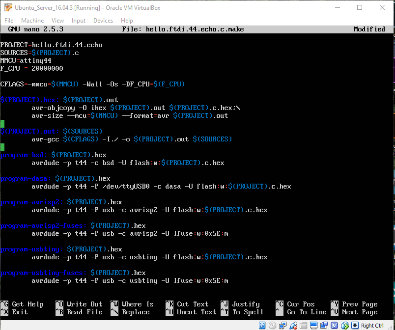
Now we can go ahead and execute the following script, by means of which we will first generate the necessary files to install the firmware for the necessary MCU:
sudo make -f hello.ftdi.44.echo.c.make
After which we can go ahead and install the firmware generated by calling the program:
sudo make -f hello.ftdi.44.echo.c.make program-usbtiny-fuses
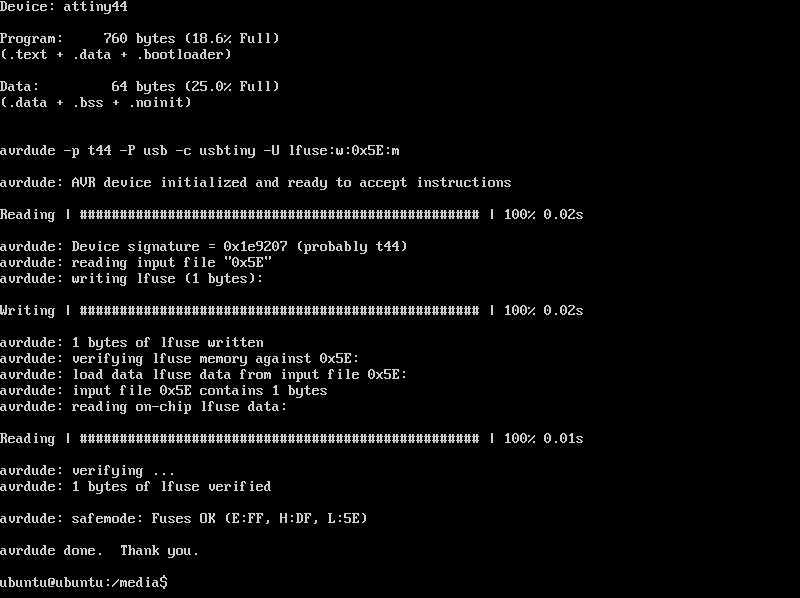
As a result we prepare our board for later programming.
Aftermath.
One thing to keep in mind is this work was accomplished by means of Virtual Machine environment, which is not recommended as some issues connecting to the board were encountered. If possible, simply use a MAC or a Linux OS.