Week 5

PCB Milling
This week is the electronic production
week..I am so excited to do all these things.Prof. Neil introduce different PCB fabrication methods and In our fab lab we used PCB millin g technique.
The assignment in this week was to make a fab ISP using PCB miller and soldering the components.
In-system programming (ISP), also called in-circuit serial programming (ICSP), is the ability of some programmable logic devices, microcontrollers, and other embedded devices to be programmed while installed in a complete system, rather than requiring the chip to be programmed prior to installing it into the system.
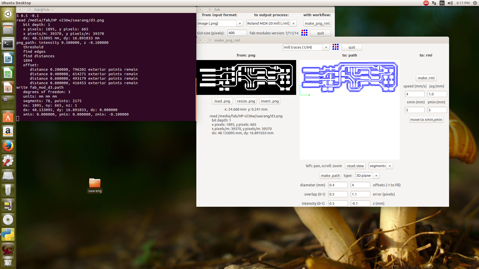
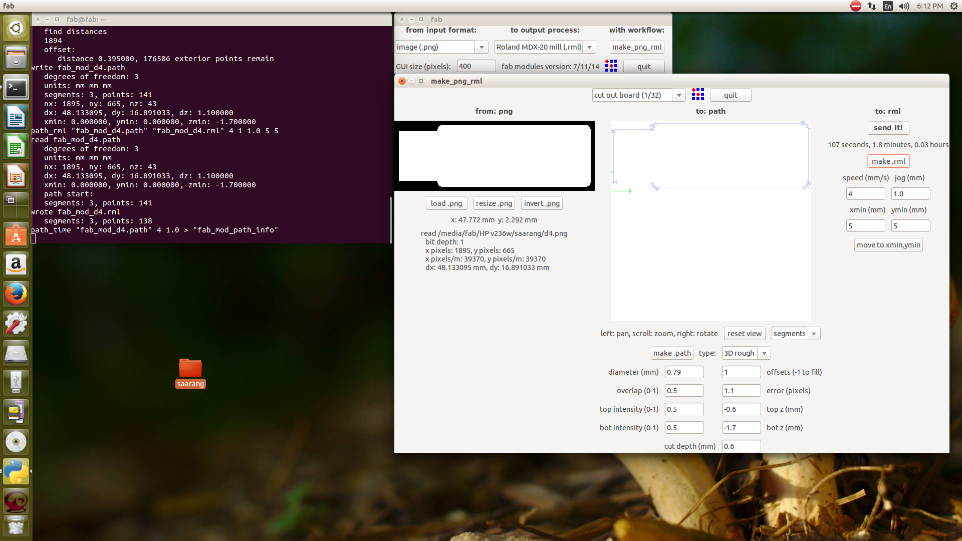
The FABISP is an in-system programmer for AVR microcontrollers, designed for production within a FabLab. That is, it allows you to program the microcontrollers on other boards you make, using nothing but a USB cable and 6 pin IDC to 6 pin IDC cable.The FAB ISP production files are already available in the Fab academy archives, I downloaded the files from Fab academy archieves.To mill the Hello echo world board first opened it in eagle,which is a PCB designing software.Next step is to mill the PCB.For milling the PCB we used modela in our lab.Modela is a PCB milling machine,which can be controlled by fab modules .The fab modules which accepts the .png extention file and next we move to mill the pcb, for that open Fab Modules and give .png as the input format, select modela as the machine. Then load the traces .png file and then make path. Leave the settings as such.
I learned how to mill the PCB using miller and learned fab module also. I learned how to solder the components in the PCB.First it was very hard to solder but the instrustors thaught me.
what are the important parts in a ISP
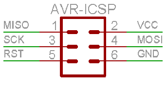
In here MISO,MOSI, and SCK are the most importent.
In SPI system , there will a main Module act as a Master and some peripheral act as Slave.when master need to send some data/need to communicate with slaves ,the MOSI channel will be activate based on the SCK(Serial Clock),so the communication will happen in givin Clock time , all the slave will be act as a Input and Master act as Output so the Master can give Instruction ,like this if the slave need to communicate to the Master they can use MISO that's means the Master can be act as Input and Slaves will be act as Output ,therefore Slave can give Feedback to the Master . In this week we don't need to design any of the Circuit board , jut need to make our own FabISP verisons.
fabricating the pcb
We got all the PCB designes so no need to design one,after the design we need the Fabricate the PCB, there are Several methods.like PCB chemical etching ,Photoresist PCB laminates and PCB Machine Milling.In here we are using PCB Milling, milling is the process of removing areas of copper from a sheet of printed circuit board material to recreate the pads. We will be focusing on the Milling process.
details about the modela michine
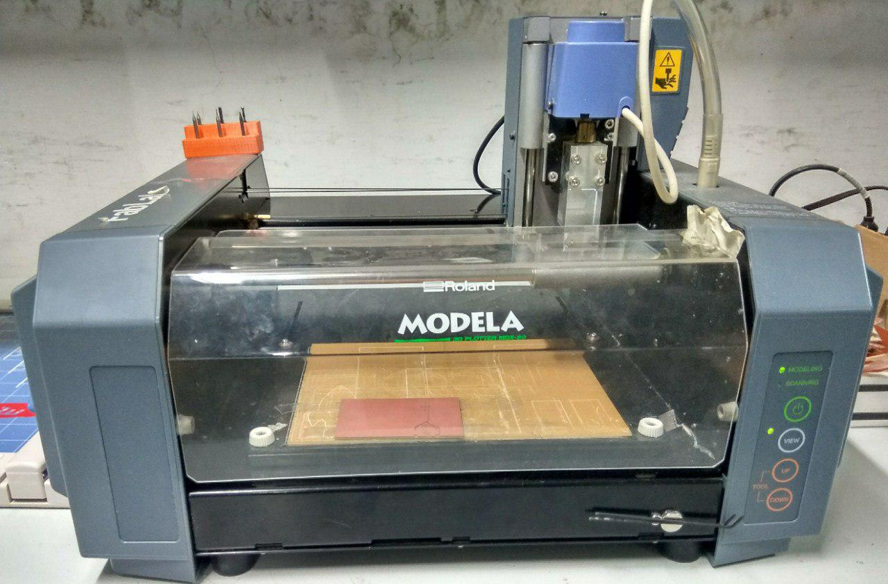
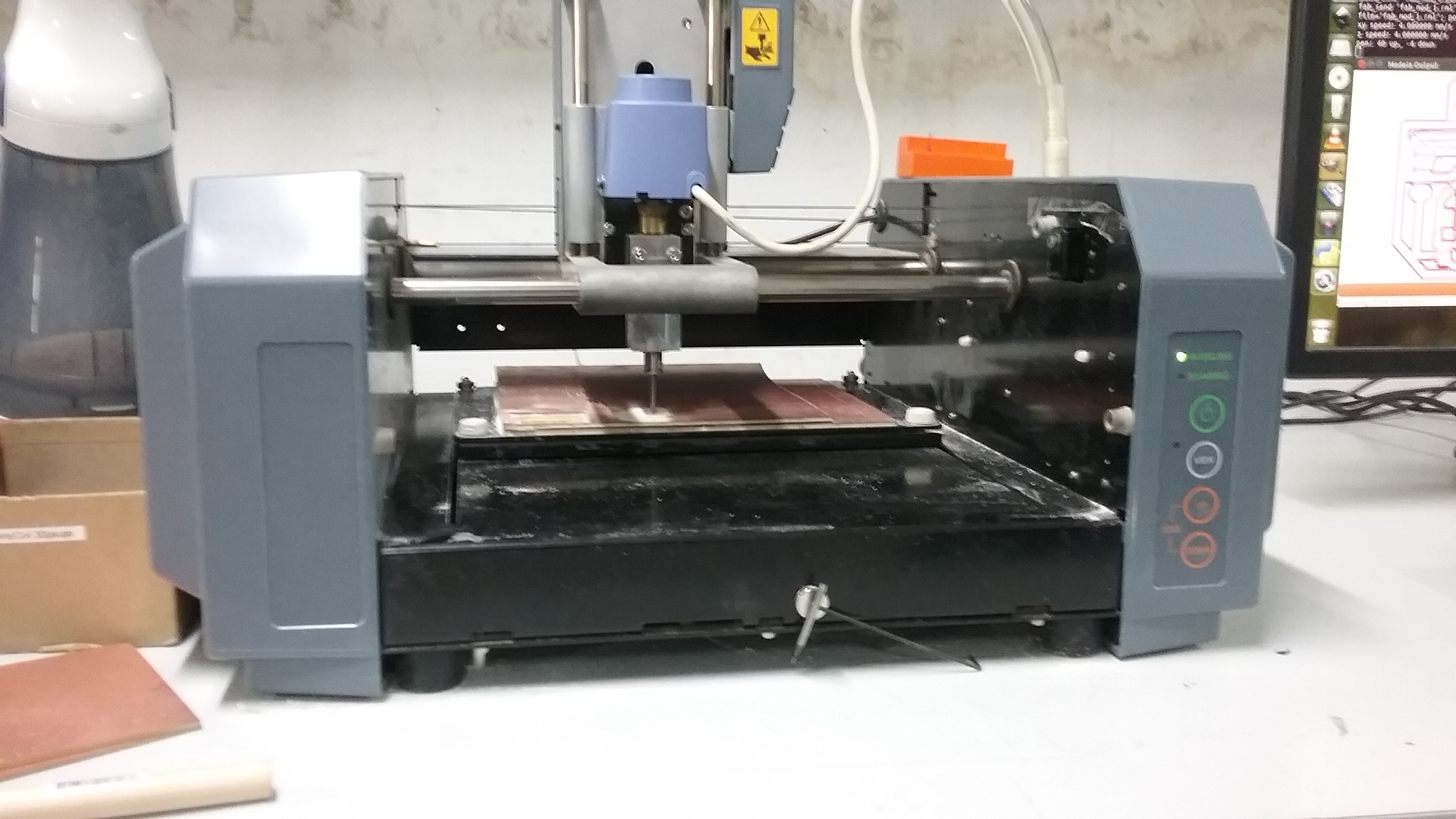
In Our Lab We have the Modella MDX 20 to machine our PCB. Modella is a Desktop milling machine that is capable of milling wood, wax, MDX,and circuit board blanks. It is compatible with most of the 2D and 3D CAD softwares. It has a small bed which moves in the Y-axis, a Tool head which moves in the X-axis and the end effector which moves in the Z-axis. It supports many milling bits and is versatile. The machine itself has a tiny foot print and can be placed on a table.
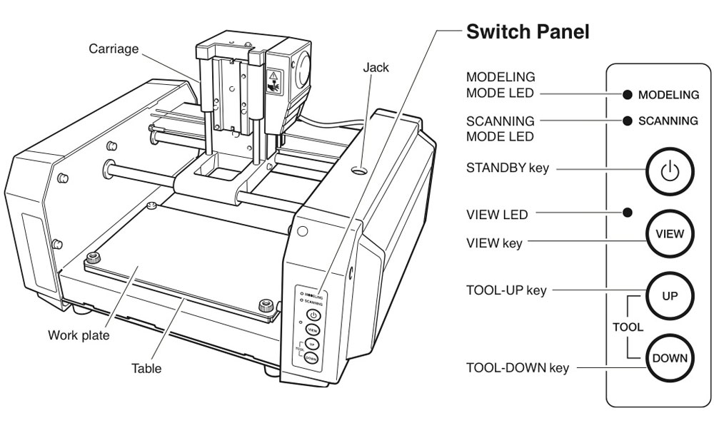
We use the fab modules to give commands to the Modella and run the cutting program.we need to set the X,Y and Z axis manually.take care in removing the milling cutters and correcting the zero setting.
Modella is like an ordinary 3-Axis CNC machines, Each axis is driven by a stepper motor and the cutting program tells the machine where to go by giving coordinates by G.code to the machine in real time.
The Fab Module software will convert .png image in to a we series of tool paths, these tool paths are defined by their coordinates and G-code. The .png image is a black and white layout of the board, and the black portions will be milled and the white portion is where the copper will be left.
We have two processes in making a PCB, The first one is milling the traces to get the circuit board pattern, and the second is cutting out the board from the base copper clad.
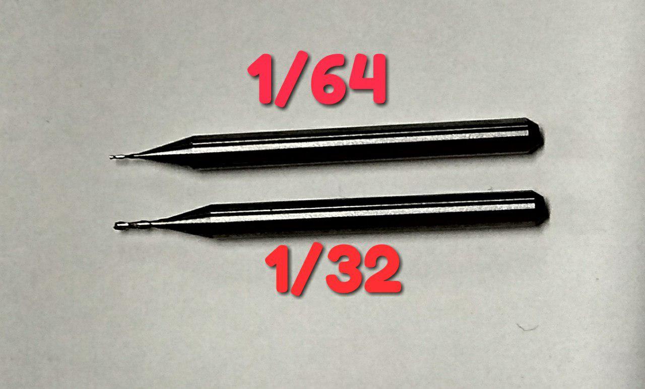
For milling traces, we use the 1/64th inch (0.4mm) bit and for cutting 1/32th (0.8mm) inch bit.i'll examplain all things one by one.
setting up the machine
1.First Make sure to use some Sacrificial material on top of the bare metal base , it will prevent the damage of bit or the machine’s table.
2.Check the Drilling bit's , first we need mill the trace then cut,and make sure to use the correct bit.when we start to mill trace check the bit because the previous person will cut his board with cutting bit and that will be the default when we start to work.
3.Fix the PCB on top of the Sacrificial layer, better to use a double sided tape
4.For tighten the bit ,first click view then the table should come out and the head will move to the far right,now load the bit you want to use, for milling traces, we use the 1/64th inch bit and for cutting 1/32th inch bit. Now insert the bit and use the Allen key to tighten the screw. Make sure it is tight on both sides.
5.For Move the (0,0) Position click the View mode again.
6.Now Set the X'axis and Y'axis for by clicking on move to Xmin and Ymin on the Fab Module.
7.Set Z'axis by using Up and Down on the Control panel.
8.Before starting Milling check your speed and depth settings and the tool position on the fab modules window.
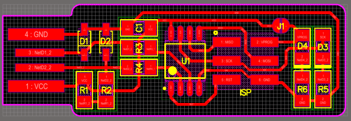
circute of the pcb
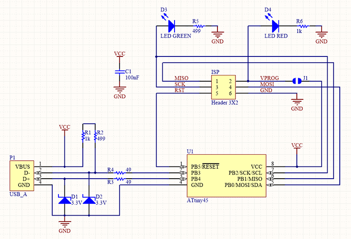
diagram of isp with all the components
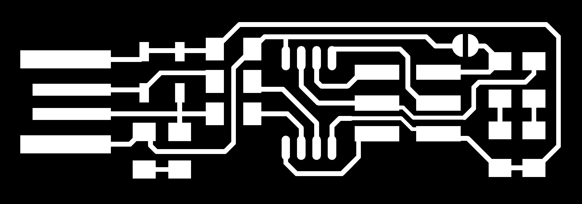
trace of isp
cut of isp

steps to make a pcb
1.Design the PCB
2.Mill the PCB
3.List the components and take it
4.Solder all the components to the PCB
I took the fab modules to mill the PCB
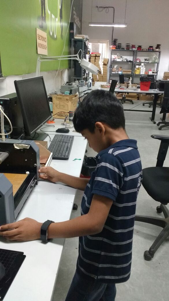
milling the board
components I took for soldering the ISP
when soldering is finished we need to programm it
Next step is to flash/load the Firmware into the board.First Download the firmware here I using Linux , so first we need to install avr-gcc tool-chain, type this on terminal to install tool-chian sudo apt-get install avrdude gcc-avr avr-libc make After Installtion unzip the downloaded firmware and open terminal there.
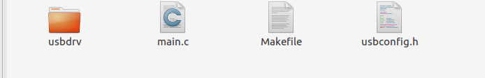
Now we can see the files , next we need to open the Makefile for ensuring it's configured for the ATTiny.i used nano to open the file,just type nano Makefile.
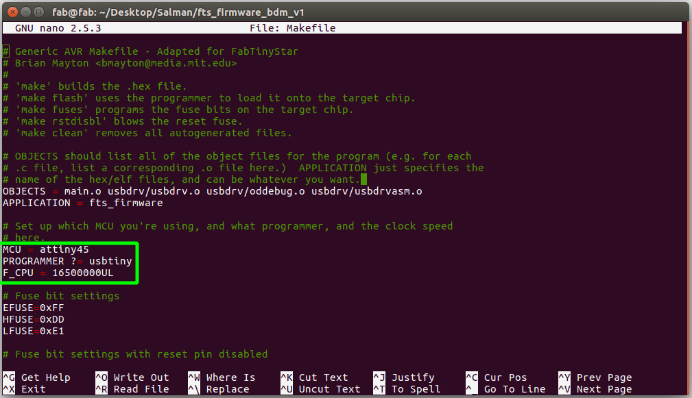
Now we can confirm that, it's configured for the ATTiny
Before falshing make sure we are shorted the Progarmming Jumber on our PCB. and also make a Connector for ISP header.
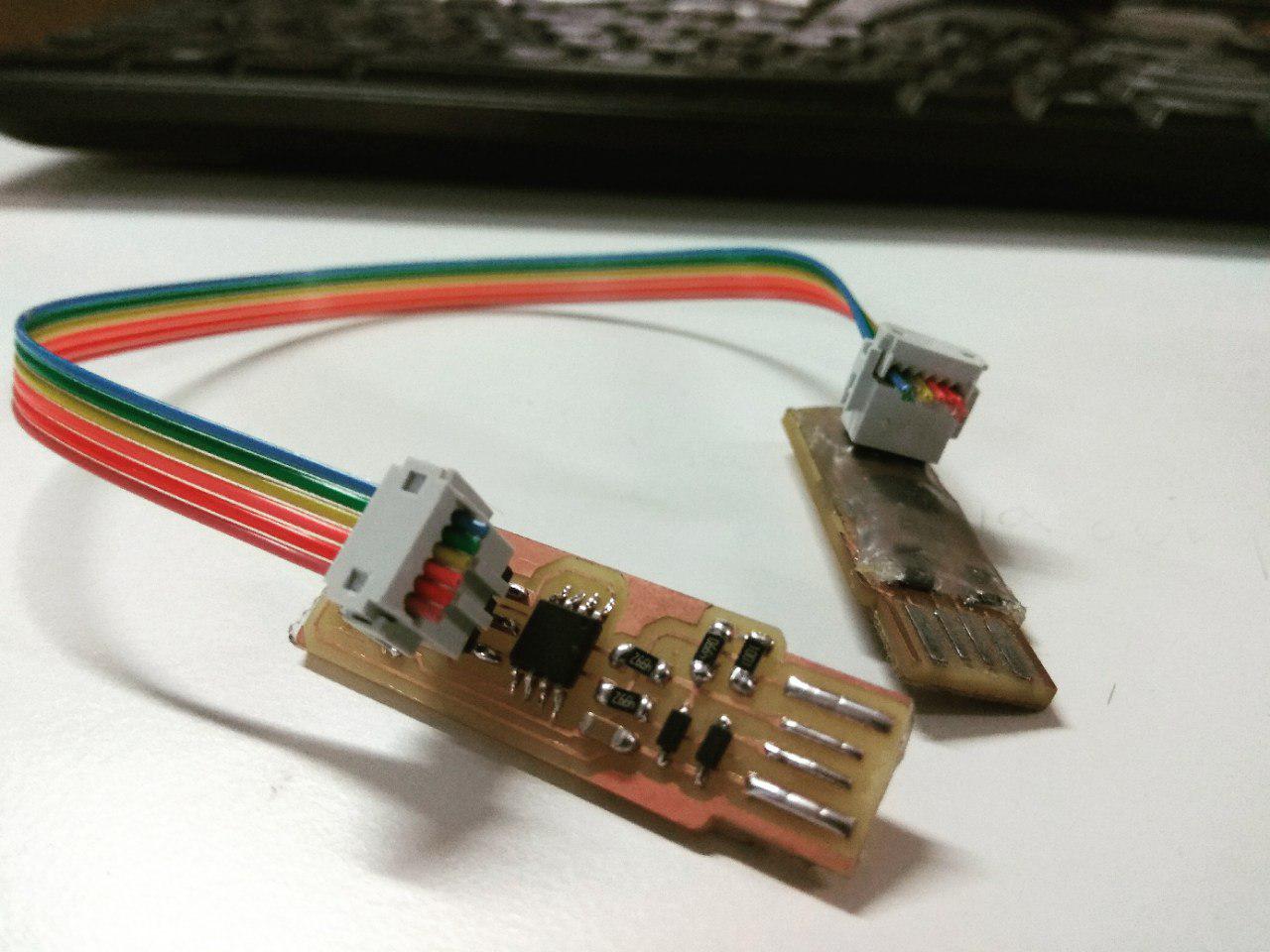
We need another Progarmmer for Progarmme the ISP Progarmmer , i used a previous student ISP to flash my ISP firmware.
Now we are ready to flash. In terminal (at the firmware file path) type Make to Genarate the hex for flashing.

Now we can see some new files,that was automatically genarated make file script.
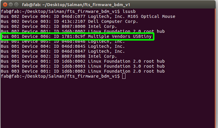
Now Connect the Old ISP and connect to our new ISP. and check the new ISP was detected in Computer by Typing lsusb.
Now we are ready to flash.
Type make flash to flash the firmware to new ISP.
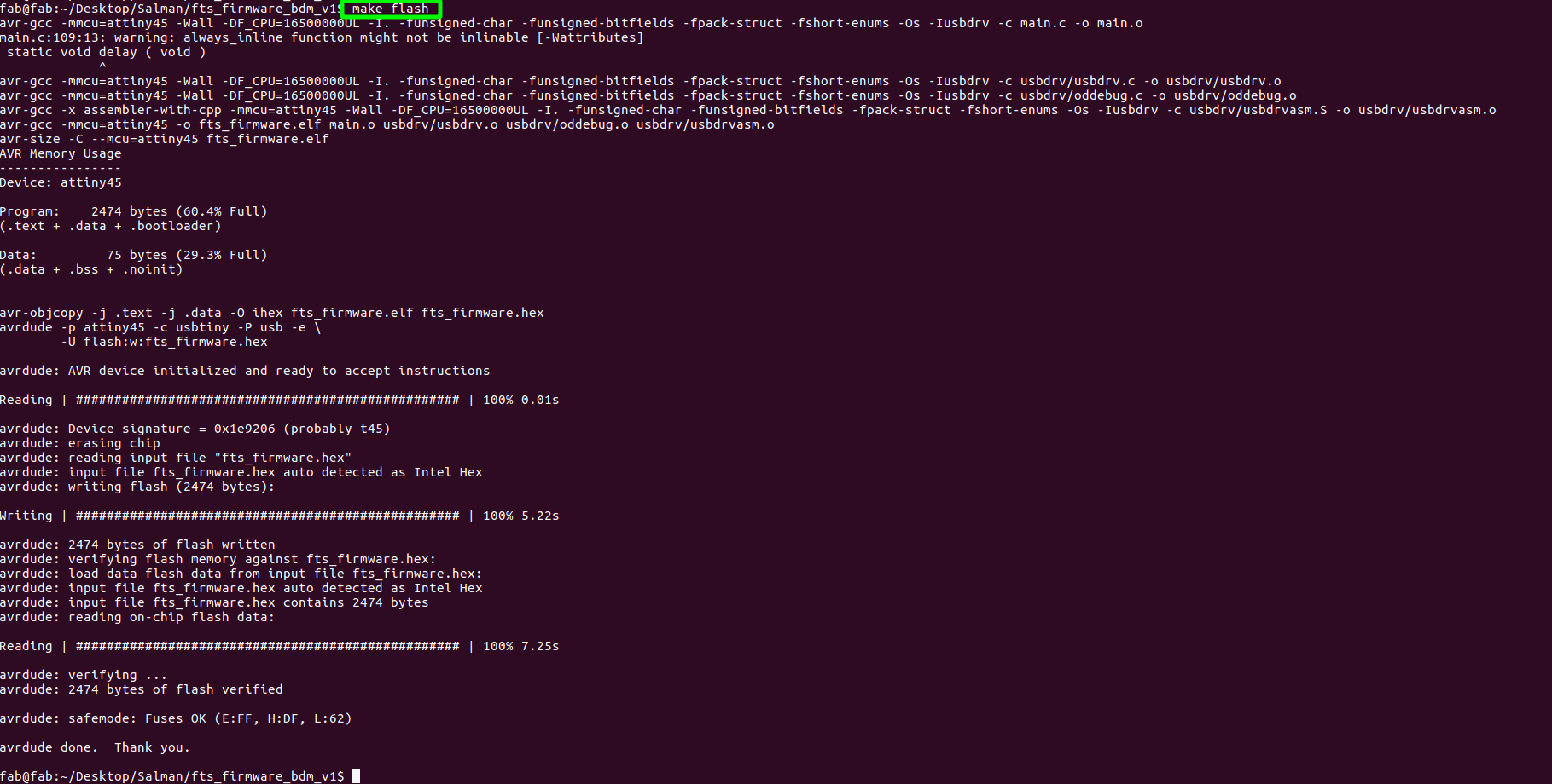
Now we are successfull flased.
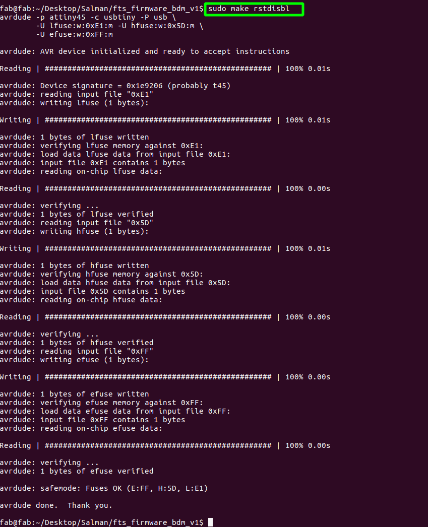
We need activate the fuse in order to act our ISP as a progarmmer.For activating fuse make fuse it will automatically , activate the fuse.After the Flashig we need to remove the jumber
Removing the jumber is not mandatory, we can also do that by commad , make rstdisbl , it will actually disable the reset pin internally , once we done that we can't progarmmer the ISP board with new firmware.
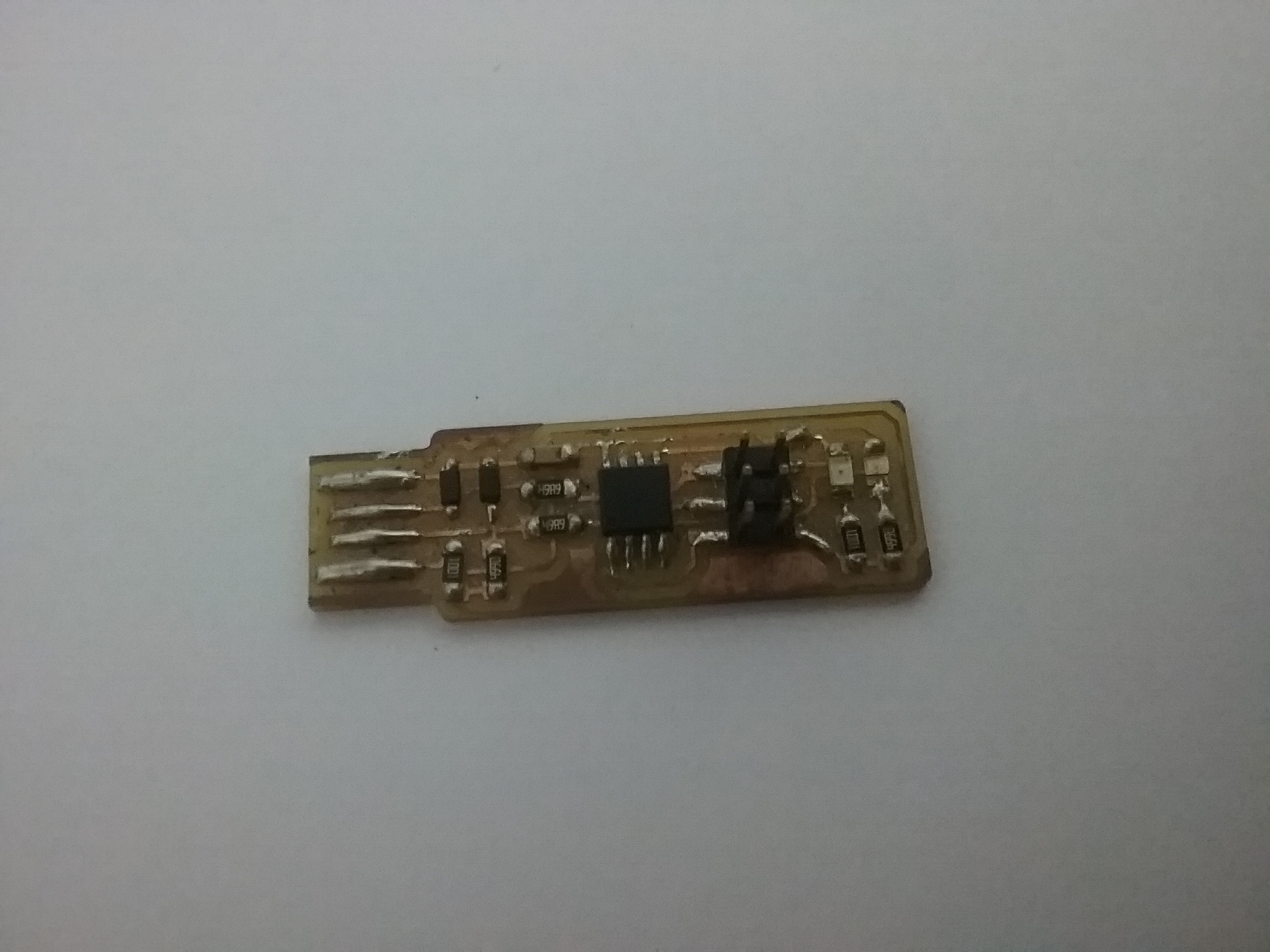
After doing every thing I got this!