Make an in-circuit programmer by milling the PCB (program it, so that you can use it to program your board in Electronics Design week, and in other weeks)
Optionally, trying other processes.
Describe the process of milling, stuffing, de-bugging and programming
Demonstrate correct workflows and identify areas for improvement if required
Shown how you made and programmed the board
Explained any problems and how you fixed them
Characterize the specifications of your PCB production process (#production_process)
Make an in-circuit programmer by milling the PCB, then optionally, trying other processes. (#production_process)
Describe the process of milling, stuffing, de-bugging and programming (#stuffing)
Demonstrate correct workflows and identify areas for improvement if required (#workflow)
Shown how you made and programmed the board (#programming)
Explained any problems and how you fixed them (#problems)
Included a ‘hero shot’ of your board (#heroshot)
_____________________________________________________________________________________
This week I machined a circuit board named "Brian". This circuit board, an ISP (In-Systems Programmer), will be used later in class to program other circuit boards we will be fabbing.
I have lots of experience with CNC milling. I am a certified Heidenhain CNC Integrator, so I know my way around large-size commercial systems, spindle drives, servo motors, PLC's limit switches, linerar encoders, angle encoders, and touch probes. However, I have never used a desktop CNC mill, nor have I ever designed, milled, or assembled a circuit board before, so this is a somewhat new experience for me. However, I still understand that this is a three-axis cnc mill. However, some people would argue that it is not a machine tool mill, rather a router, since it operates stepper-motors and has no true position feedback system.
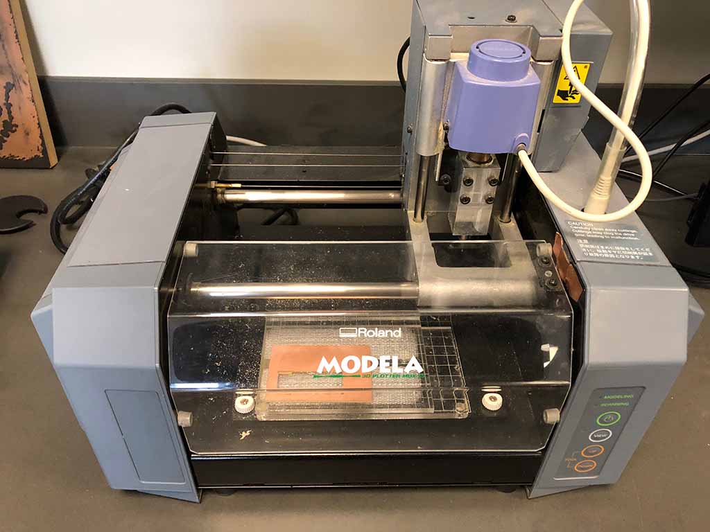
My instructor, Scott Zitek, introduced me to the Modela MDX-15 mill to produce the circuit board.
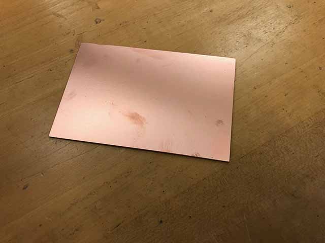
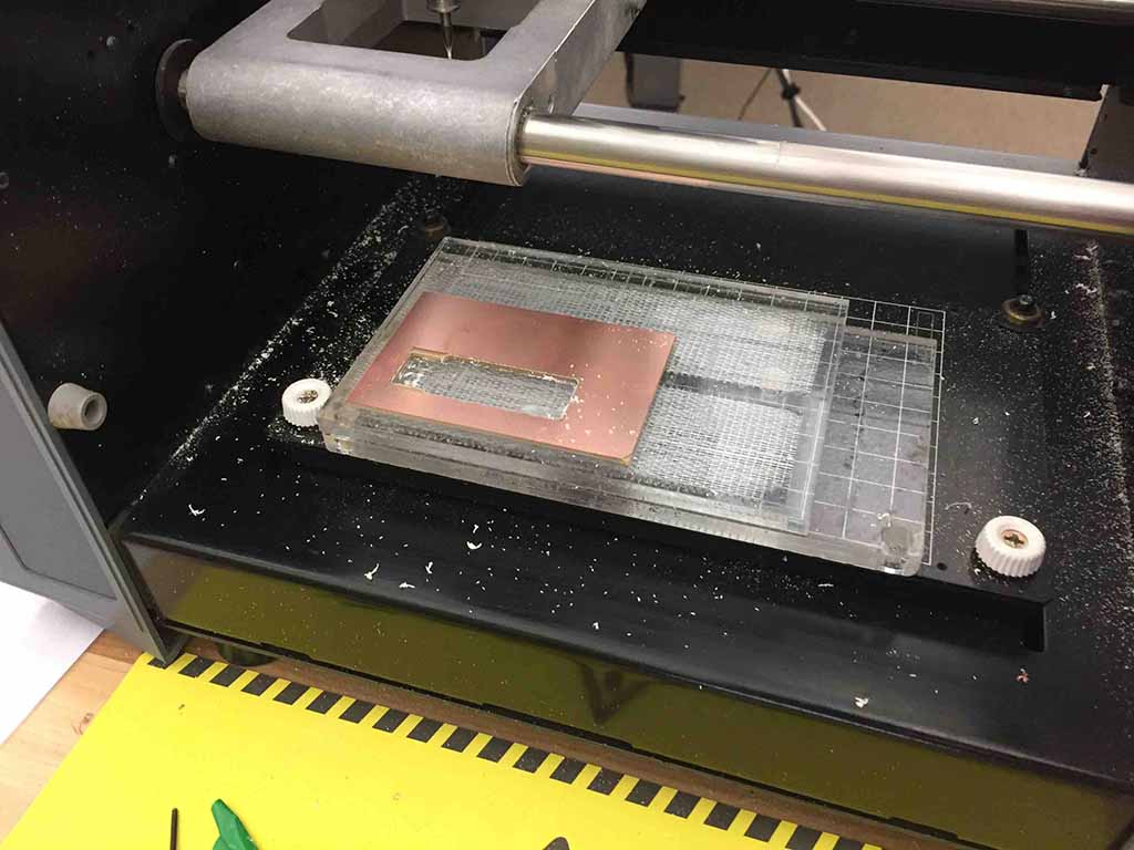
The material to be milled is a copper clad board with a paper-based substrate. The technical term for this type of board is FR2. My instructor explained to me that fiberglass based substrates make much better and durable circuit board. However, they dull the cutting tool quickly.
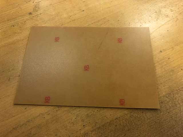
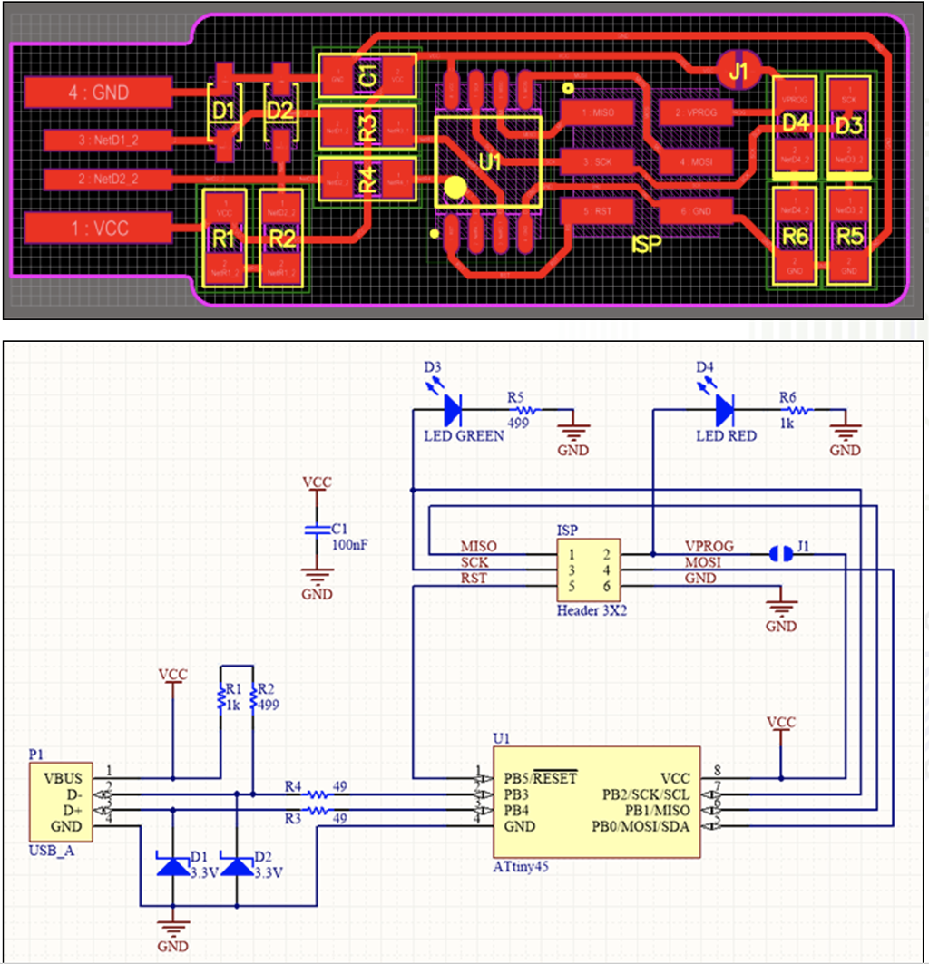
Scott unlocked the toolbox next to the desktop cnc mill, and provided me a roll of double sided tape and a blank PCB blank. I cleaned the bed of the machine, applied the tape to the backside of the "workpiece". Scott next explained to me that we would be going with the "Brian" design because the components necessary for "Brian" were on hand at the lab. The steps I was to take was to: (id='workflow')
In order to accomplish the above, follow the tutorial on Brian's ISP page, which can be found here:
http://fab.cba.mit.edu/classes/863.16/doc/projects/ftsmin/index.html
(id='production_process') In order to mill the Brian board, you need to access the fabmodules. The fabmodules run best on Linux. Lorain County Community College had a desktop set up with Linux and dedicated to the Modela MDX-15. I read through the tutorial while Scott was explaining about the "Brian" and how it was based on the FabTinyStar design that originated by a person named Zaerc..
I first downloaded the traces and outline from the fabmodules.
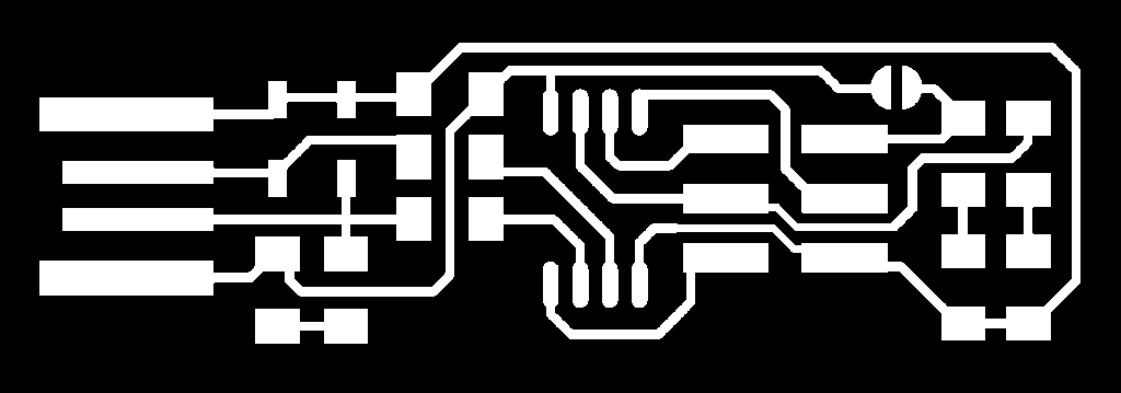
http://fab.cba.mit.edu/classes/863.16/doc/projects/ftsmin/fts_mini_traces.png

http://fab.cba.mit.edu/classes/863.16/doc/projects/ftsmin/fts_mini_cut.png
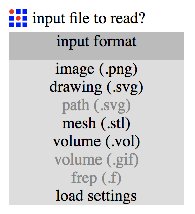
Next, use the webbrowser to access fabmodules.org. Mouse over and click "input format" to expand the menu as shown.
Next, mouse over "output format" and click.
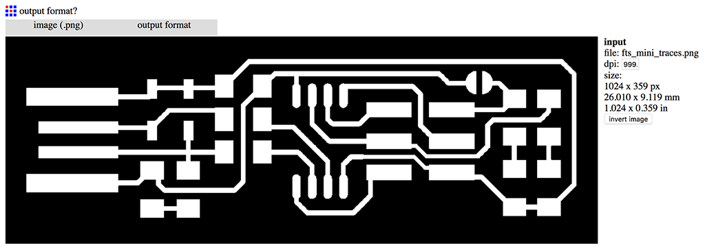
You see a pull-down menu of sorts. Next, mouse over "Roland mill (.rml)" and click. Side panel opens up, select MDX-20.
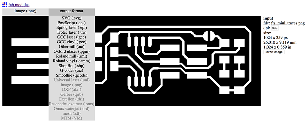
Next, mouse over "process" and click. You get another pull-down menu. Mouse over "PCB traces (1/64)" and click.
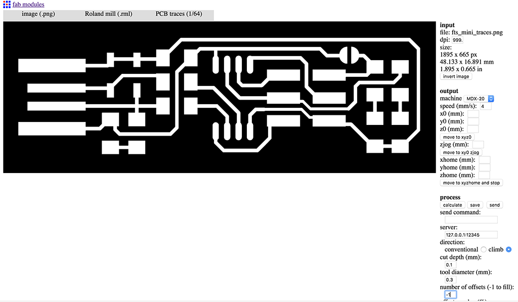
After that, you see an expanded menu in the right margin. Enter values for cut depth and tool diameter (0.3mm), offset -1 (fill), cut depth (0.3mm).
Next, press calculate. The toolpath will be drawn out. You can zoom, pan and roll the toolpath with left and right mouse actions.
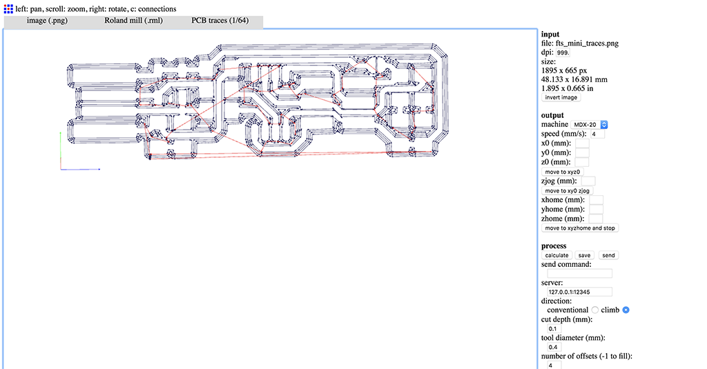
Press save. You will get typical file dialog and save your file for later.
(File for Modela: fts_mini_traces.rml)
Make sure PCB blank is secure. Place on front left of platen/sacrifical board.
Insert 1/64" diameter milling cutter into mill and clamp.
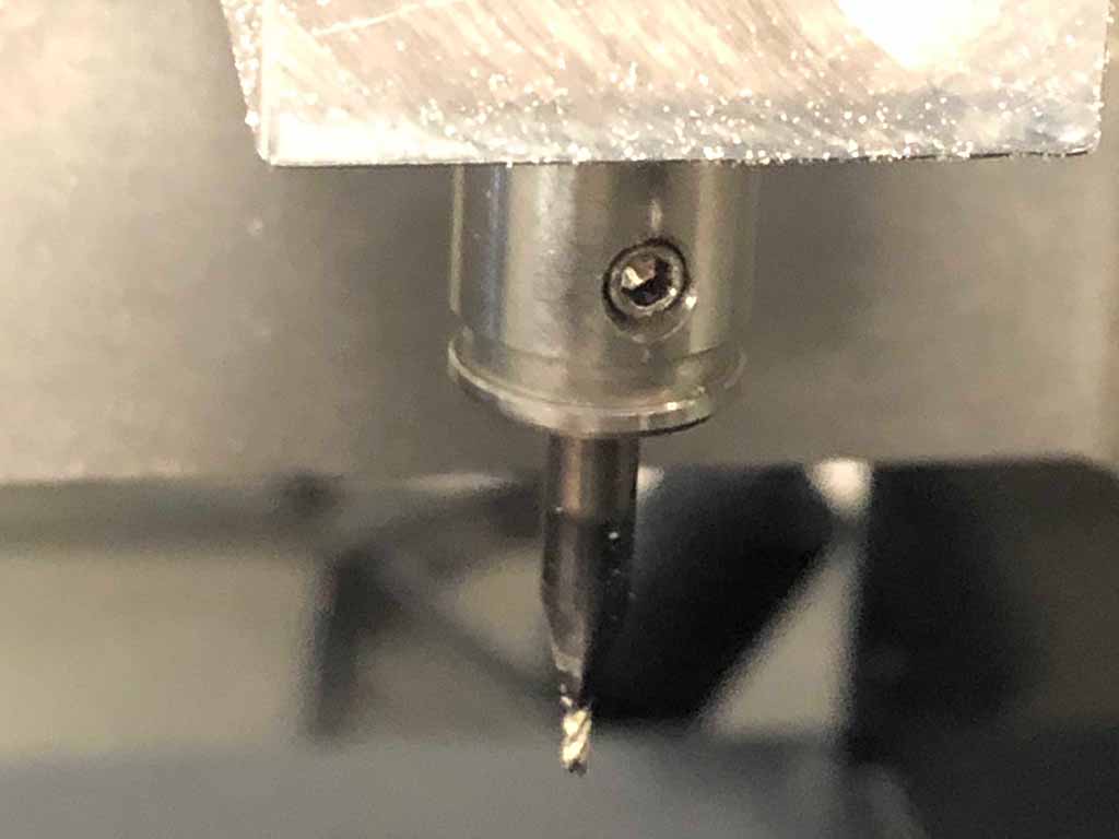
Move tool down close to part. Go to Z10, Y10, Z10. Set Z to zero. Loosen clamp on tool and let it drop to surface of board and retighten. Press "Send" in FAB modules. Mill the part out. Repeat above process for outline of board. Use the file fts_mini_cut.png for outline. Use Pcb outline 1/32" for "Process". Select MDX-20 for machine on side menu. Press "Calculate" and "Save".
(File for Modela: fts_mini_cut.rml)
Vacuum the swarf (debris), take part out of mill, clean with alcohol, remove double sided tape.
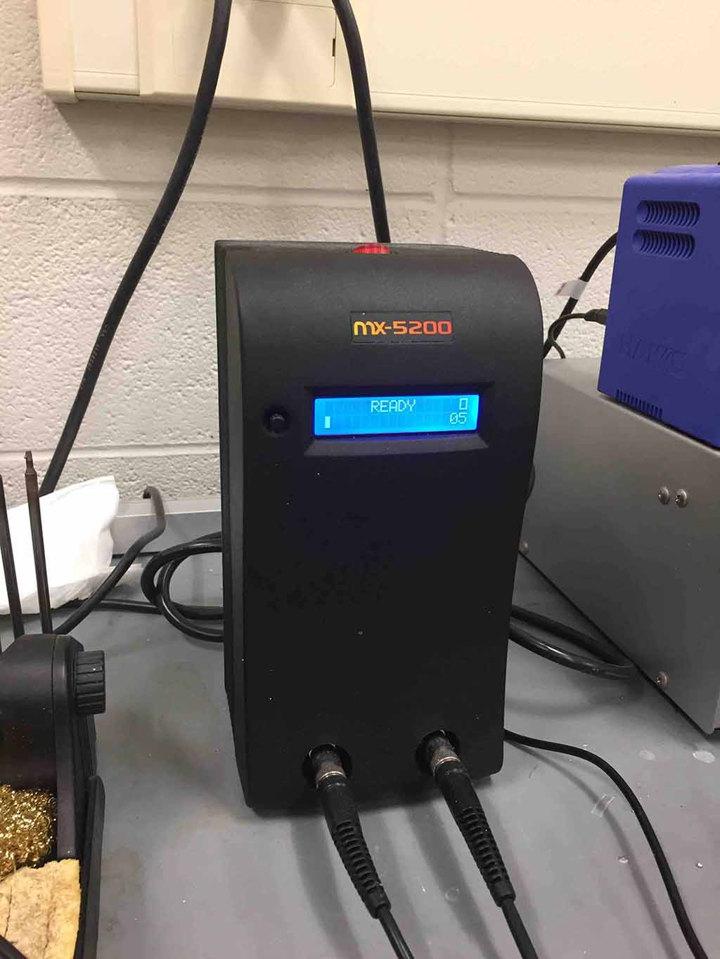
I was sent over to a different classroom for soldering, where I met Chris Rohal. Chris is a master of electornics. Chris asked me if I had ever soldered before. I have brazed and silver soldered before, but never circuit boards. Chris explained to me how an RF iron works, how to focus the microscope, use of tweezers and wick.
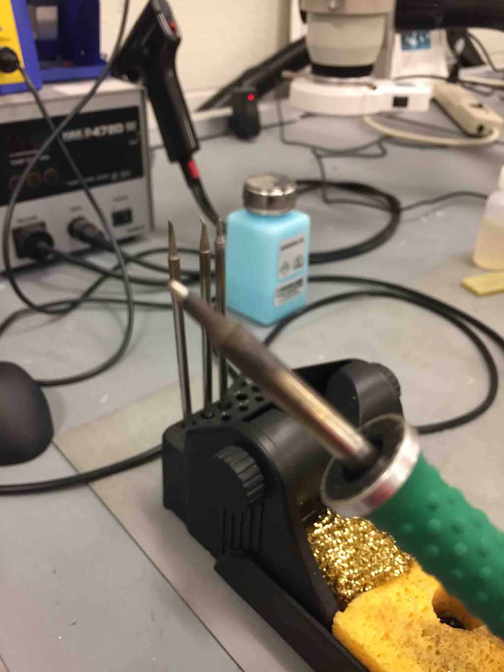
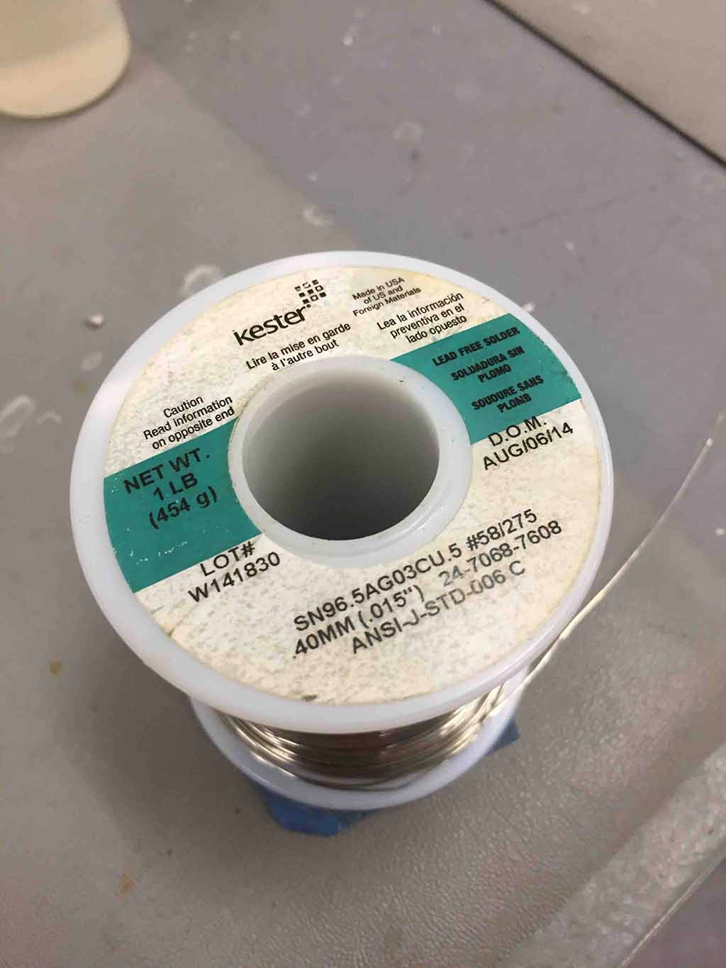
Chris gave me a practice board and explained how most surface mount components have a film of tin on them already. He showed me a technique of holding the iron down dry on a leg of a component so it wouldn't move, and then go around the rest of the component with really thin (0.015") solder.
Under the microscope, everything was fine. He showed me to wet everything with flux first, especially before tacking down a component. Then he explained that I should lay the rod along the side the edge of the component leg and heat and let it flow. This was a very rewarding lesson. I did well soldering, and Chris was happy with my work.
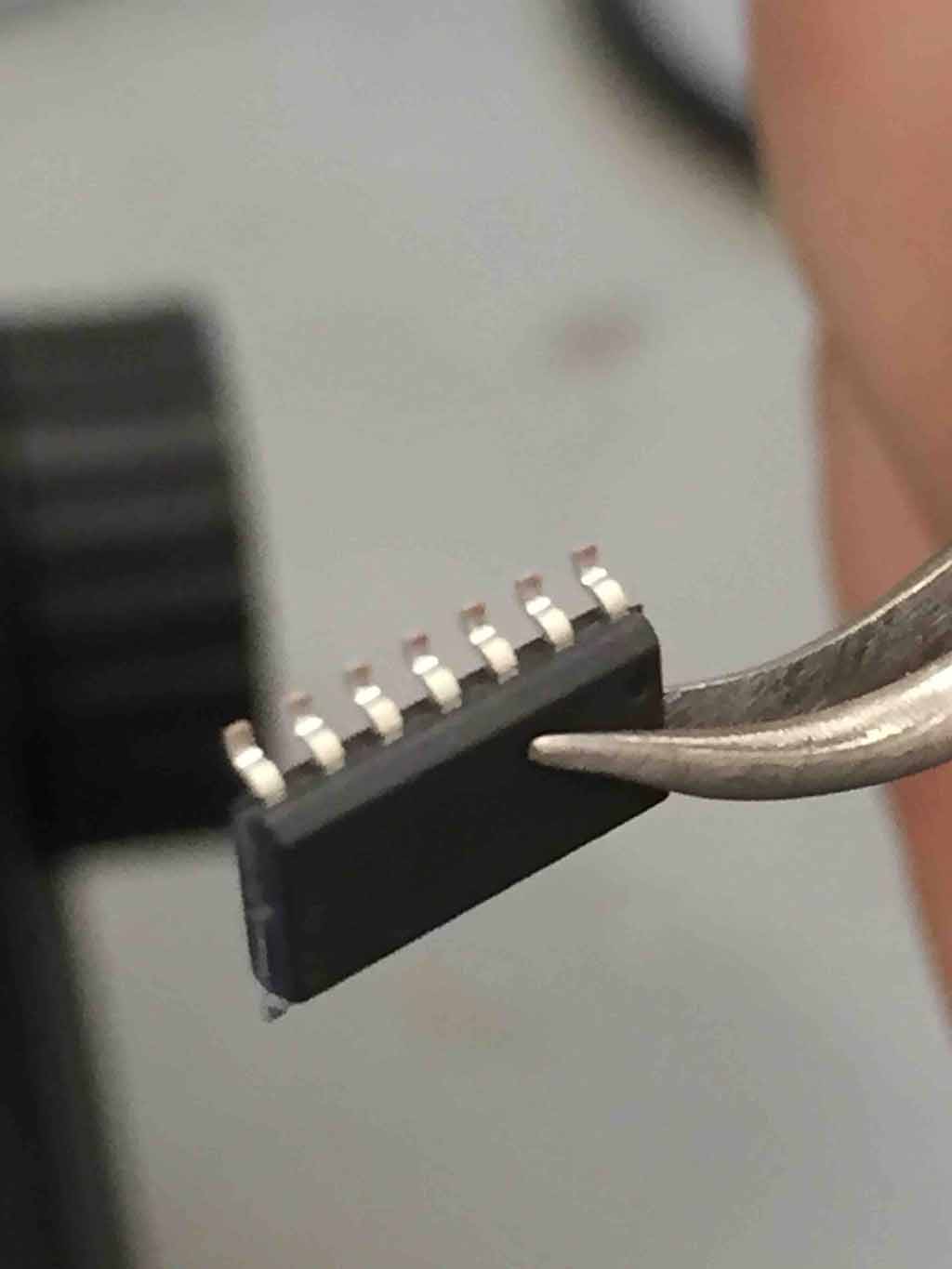
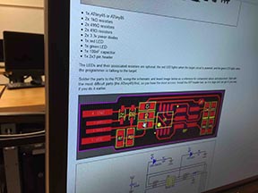
(id='stuffing') Next, I went into a room where all the electronic components were on reels and anti-static envelopes. I had a pretty good understanding of what capacitors, diodes and resistors were. I also knew how to read an electonics diagram. Chris explained that as I gathered my components, I should write the name of the component and tape it down to the paper with scotch tape. I would later cut each component from the tape as I needed it. I followed the diagram I was given. Pretty straight forward.
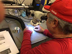
Looking through the binocular microscope.
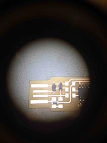
This is what the board looked like through the microscope.
Soldering complete. I checked my work. I took a multimeter and checked for continuity between VCC and GROUND. I looked through the microscope for bridges. I had Chris double check my work. All looked good first try.
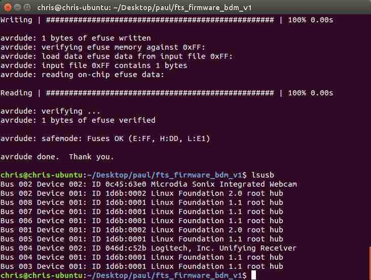
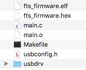
(id='programming') Next, I programmed the microcontroller using avrdude. My instructor allowed me to use his Linux laptop to perform this programming. I followed the instructions from Zaerc's website and with instruction from Chris Rohal and his toolchain. The lab had a desktop which had Linux installed, and a copy of fts_firmware_bdm_v1 and makefile was already installed and edited. If I needed to edit it, I suppose I would change "PROGRAMMER ?= usbtiny" with "PROGRAMMER ?= usbasp".
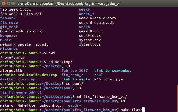
Next we connect the board to the USB and make sure it is jumpered to be programmed. No complaints from the desktop computer, so we continued. We type the command "make flash"
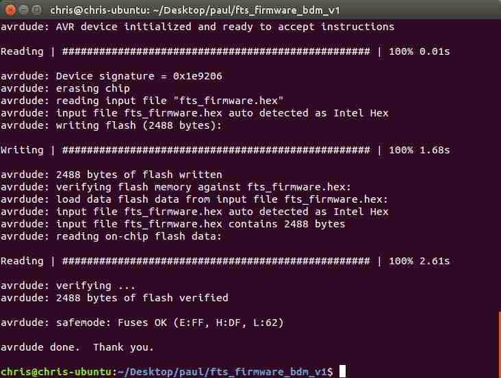
It works. Next, we run "make fuses"
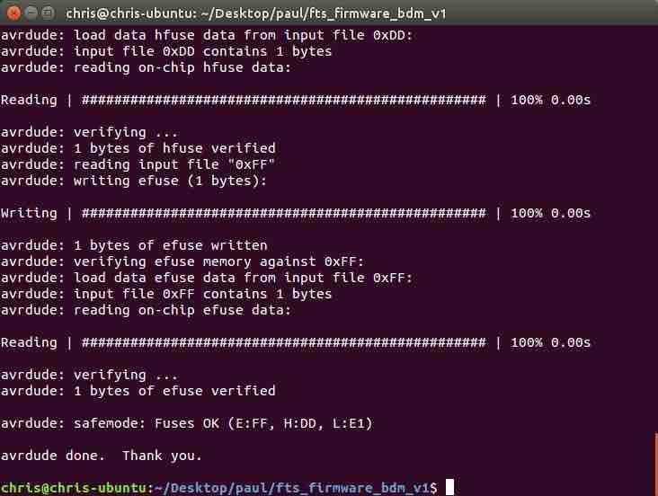
Firmware is now uploaded, and the fuses are set.
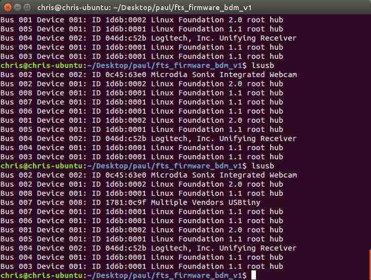
Type lsusb. This lists USB devices.
Last step is to execute the last command, "make rstdisbl" so the device cannot be reprogrammed.
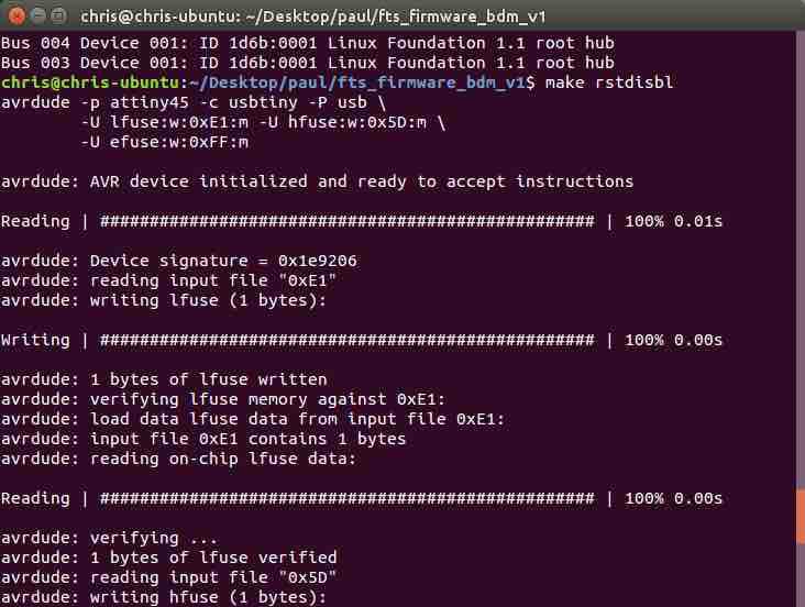
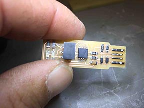
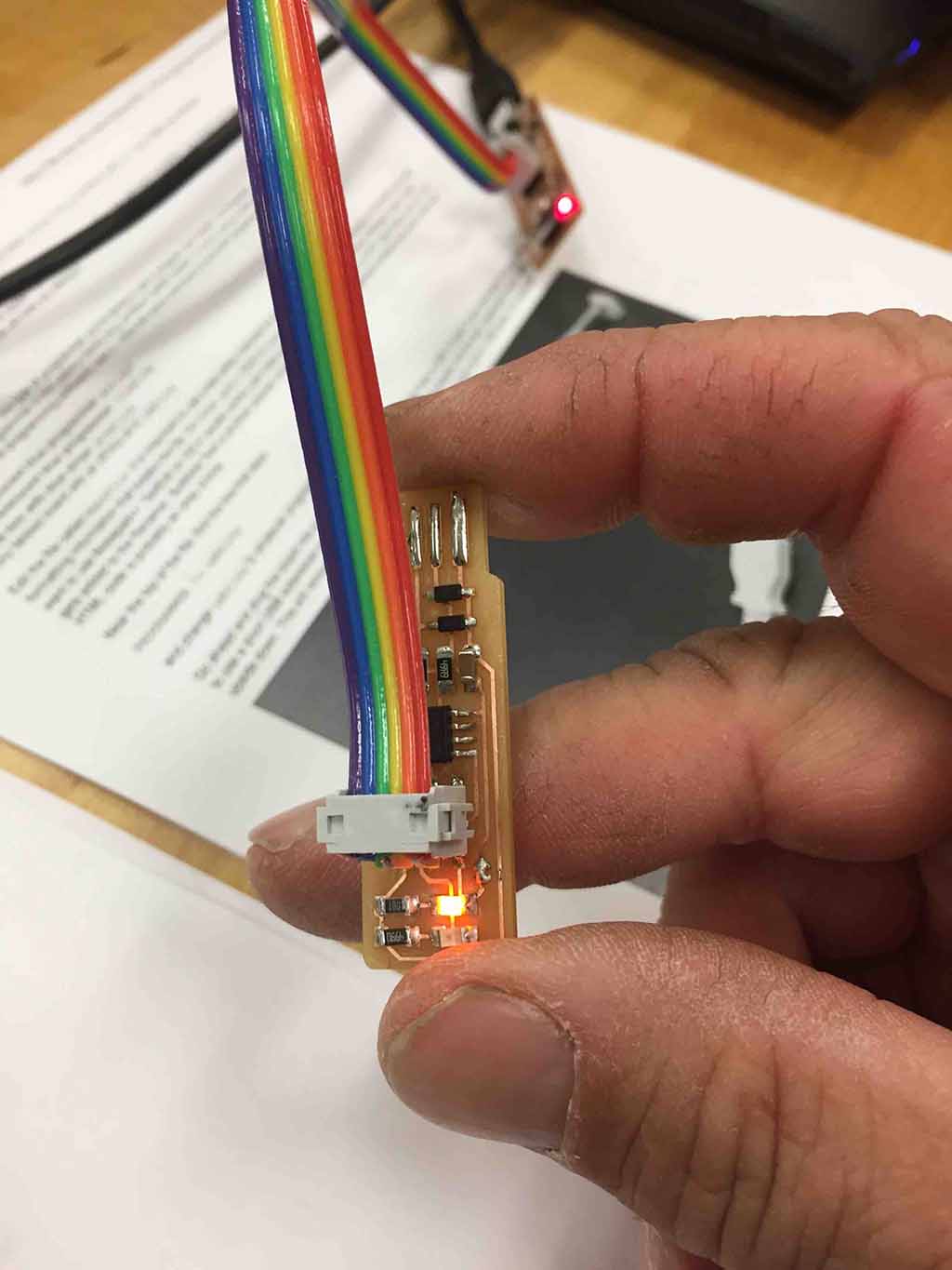
It works, so I remove the jumper. (id='heroshot')