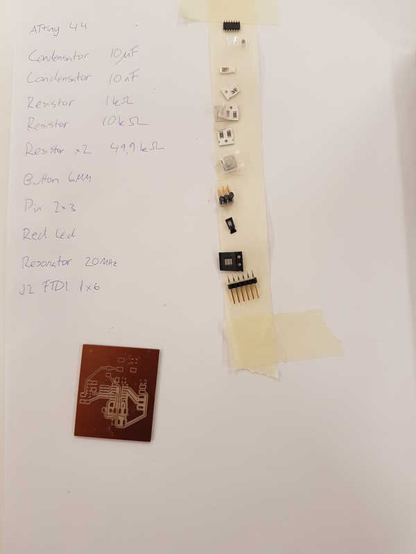
Assignment 7: Electronics design

Assignment:
Group assignment:
- Use the test equipment in your lab to observe the operation of a microcontroller circuit board
Individual assignment:
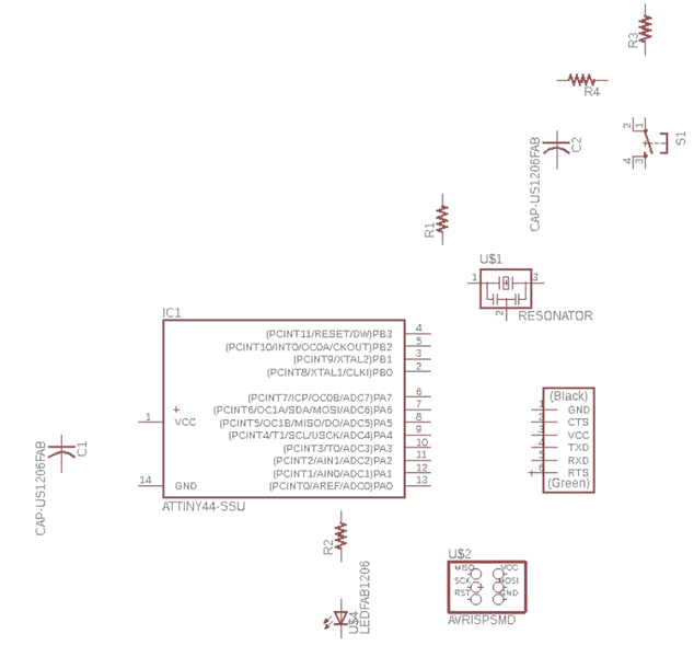
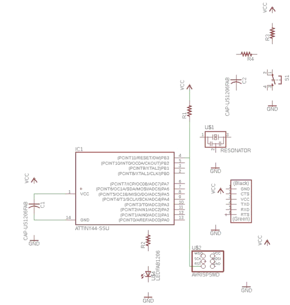
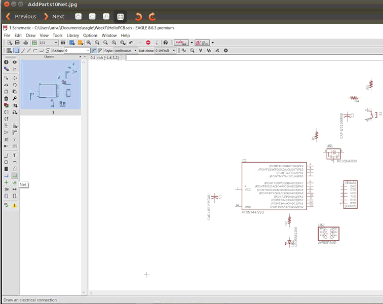
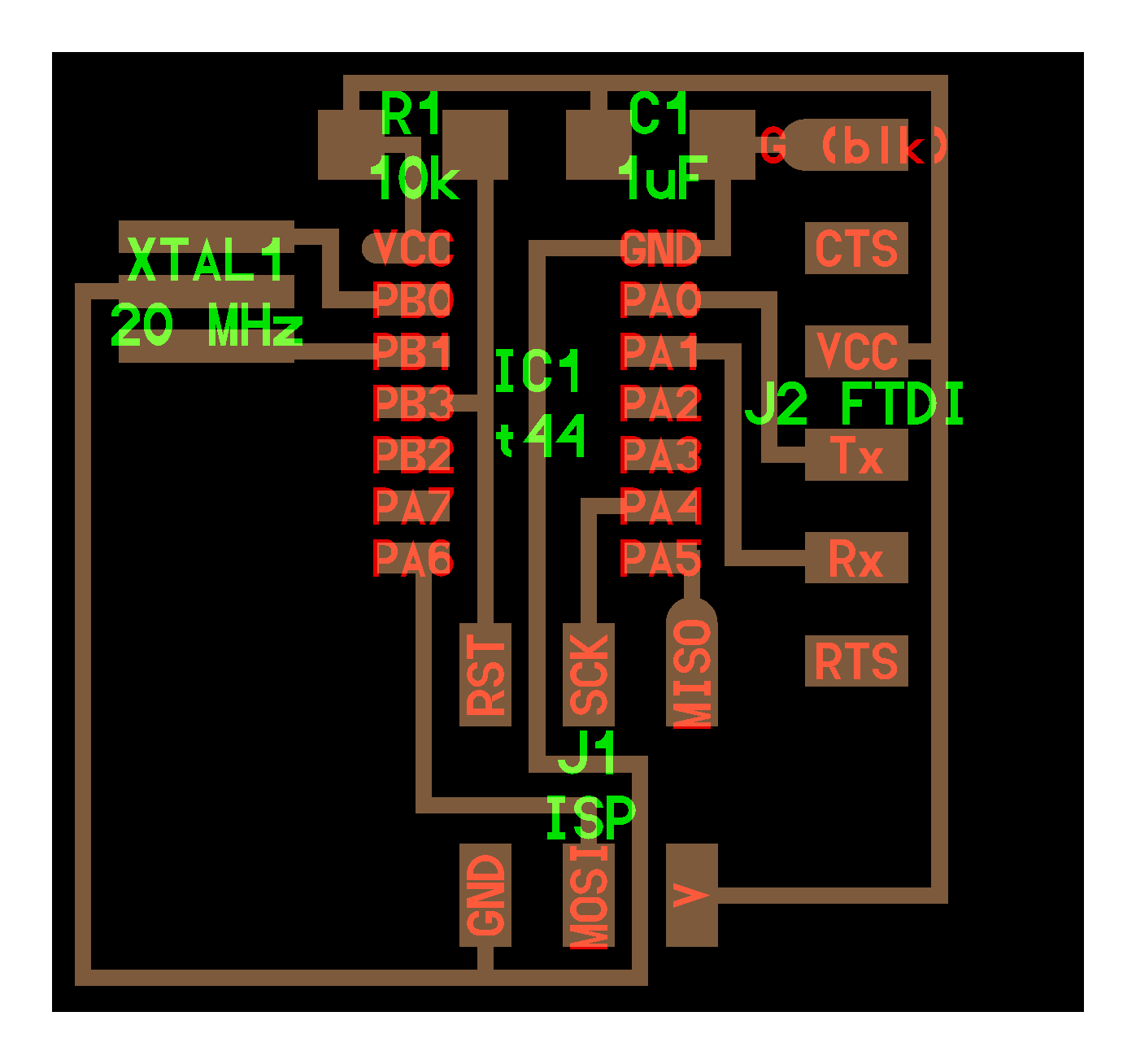
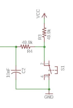
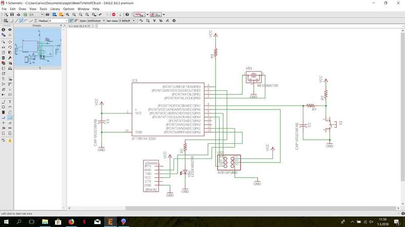
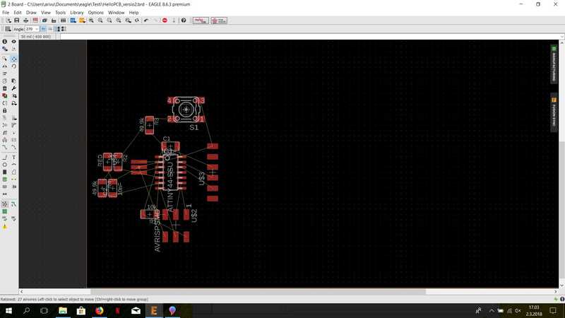
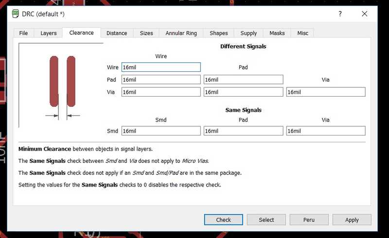
- Redraw the echo hello-world board, add (at least) a button and LED (with current-limiting resistor), check the design rules, make it, and test it
extra credit: simulate its operation
extra credit: render it

PCB designing
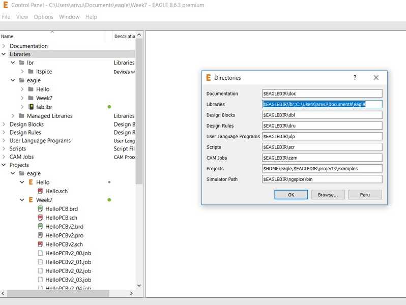
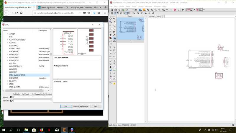
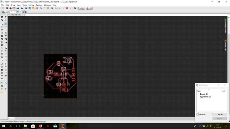
We started to learn about electronics design with our local instructor Antti Mäntyniemi at 1.3.2018 at 10 am. The program we started to use was Autodesk Eagle. We loaded the fab.lbr and added it to Eagle. To do that, you have to open Options -> Directories... and it will open paths to folders, which are used by Eagle. You have to add semi colon to Libraries and write the location of your library file after that in my case C:\Users\arivu\Documents\eagle. When you select ok the library is added to your Eagle.

Library
Now we are ready to begin the schematic creation. Select File -> New -> Project, which creates a new empty project. Right click on the created project and select New -> Schematic. This opens the schematic view. In the schematic you can change the imperial units to standard units from, View -> Grid. In there you can select mm and show the grid to make view a little bit more clear.

Grid
The components are placed on shchematic by choosing Edit -> Add... or by choosign Add from the side panel. Selecting that gives you a list of components which you can choose for your schematics. We selected the ATtiny44-SSU (surface mounted) as a first component. All the components were added one after another. You can select the components place and press left key to place it on the schematics. You can add as many of the same component as you want by just moving the mouse cursor on a area where you want it and click left mouse button. To go back to Add component list press escape key.

AddingComponents

AddingComponents
All the parts needed in the assignment are placed on the schematic in the picture. The components can be rotated (rotate tool side panel or right button) and moved freely (move tool side panel or right button).

AddingComponents
When all the parts are placed, it is time to start making connections. To make the connections more clear, you should put VCC and GND symbols from the Add. They can be found in supply1.

VCCGND
To create connections Net tool is chosen from the side panel.

Net
The connections can be seen from the Neil's hello board.

png
Only the button connections couldn't be seen from that picture, but our instructor Antti gave us instructions how to connect it. The button has capacitor added parallel to it to filter bouncing glitches, because when the button is pressed it creates extra pulses on release and disrupts the normal process.

png
It was straight forward process to add all the connections to the schematic. You can draw the connections in parts by pressing left key to add connection and then it continues from the spot you clicked the left button. This property makes it easier to connect all the parts in a useful manner, because otherwise it would be very messy looking schematic.

png
When you are happy with the connections, you can start designing the board. You can select File -> Switch to board or Generate/switch to board from the upper panel. All the compoents with their connetions presented as yellow lines are outside the board and need to be pulled on the board. The components should be pulled on the board in a way that their connections are short and in a logical order. The components can be rotated (rotate tool side panel or right button) and moved freely (move tool side panel or right button).

png
Move all the components to a desired position and you can press ratsnest button in the side panel from time to time. It calculates the shortest airwires between connections and makes the view cleaner.

png
When you are happy with your component positions, you can start using route tool to make routes for your wiring. When the route tool is selected the wire width can be selected and it should be 16 instead of the initial 6 (very thin connections). Set the DRC settings to your desired value. In my case 16 mil for all the options. This way the program will draw lines where it is possible with your given settings and you don't have to draw the lines afterwards again.

png

png

png
Move the board lines to make the board shape and size. The board outerlines can be dragged with move tool.

png
When you have finished drawing all the connections and the board size and shape are selected, you can create polygon around the board, name it GND and press ratsnest to create GND everywhere in the board, where it is not restricted by your connections.

png

png
Then you can create line around your board in the milling layer to create outlines for the milling machine. The line can be moved with moving tool.

png

png
Change the background color to white Options -> User interface Layout -> Background -> White. Then select only milling layer and File -> Export -> Image. Select the location where you want the outline file, set the resolution to at least 1500 dpi, select monochrome box and ok.

png

png
Now the outline image is created. Change the background back to black, select only top layer and similarly export the trace file for the milling machine. The trace file will have black lines surrounding the board, which can be removed with any image processing software. When this is done, your board is ready for milling.

png
Images for the milling process
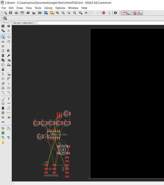
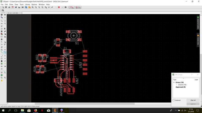
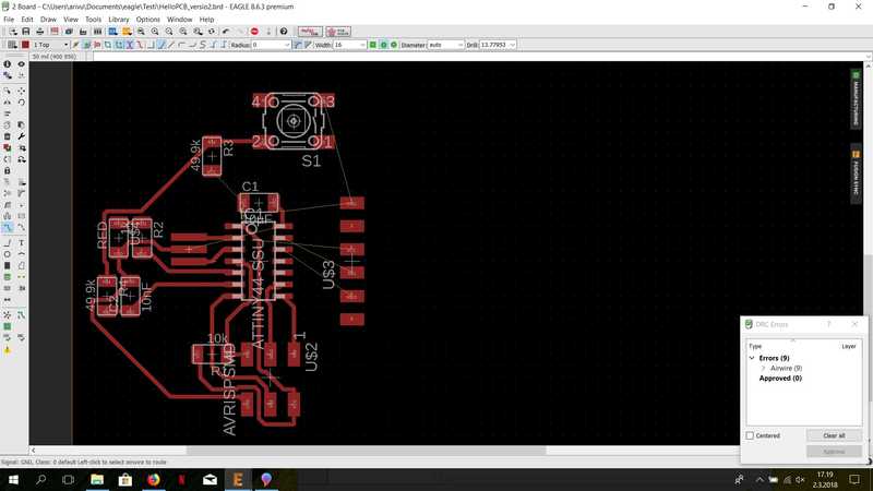
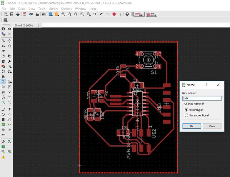
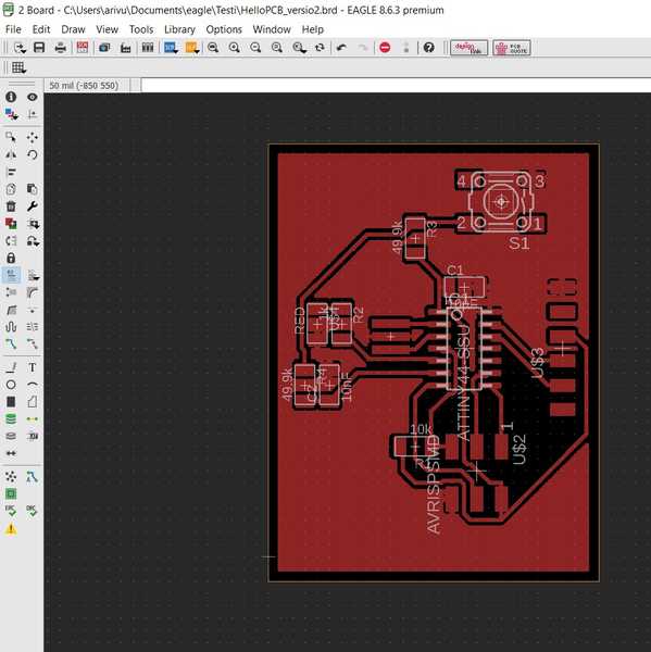
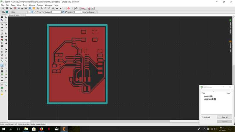
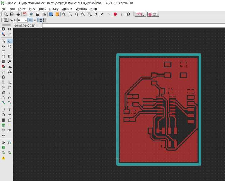
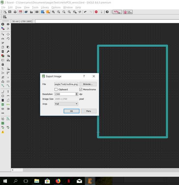
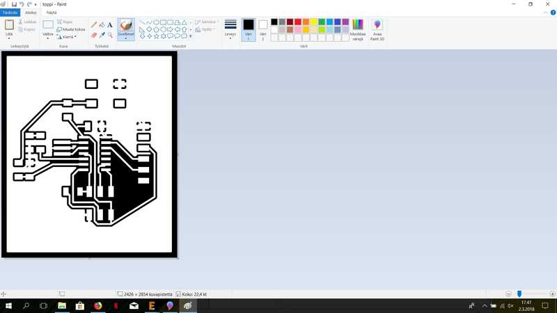
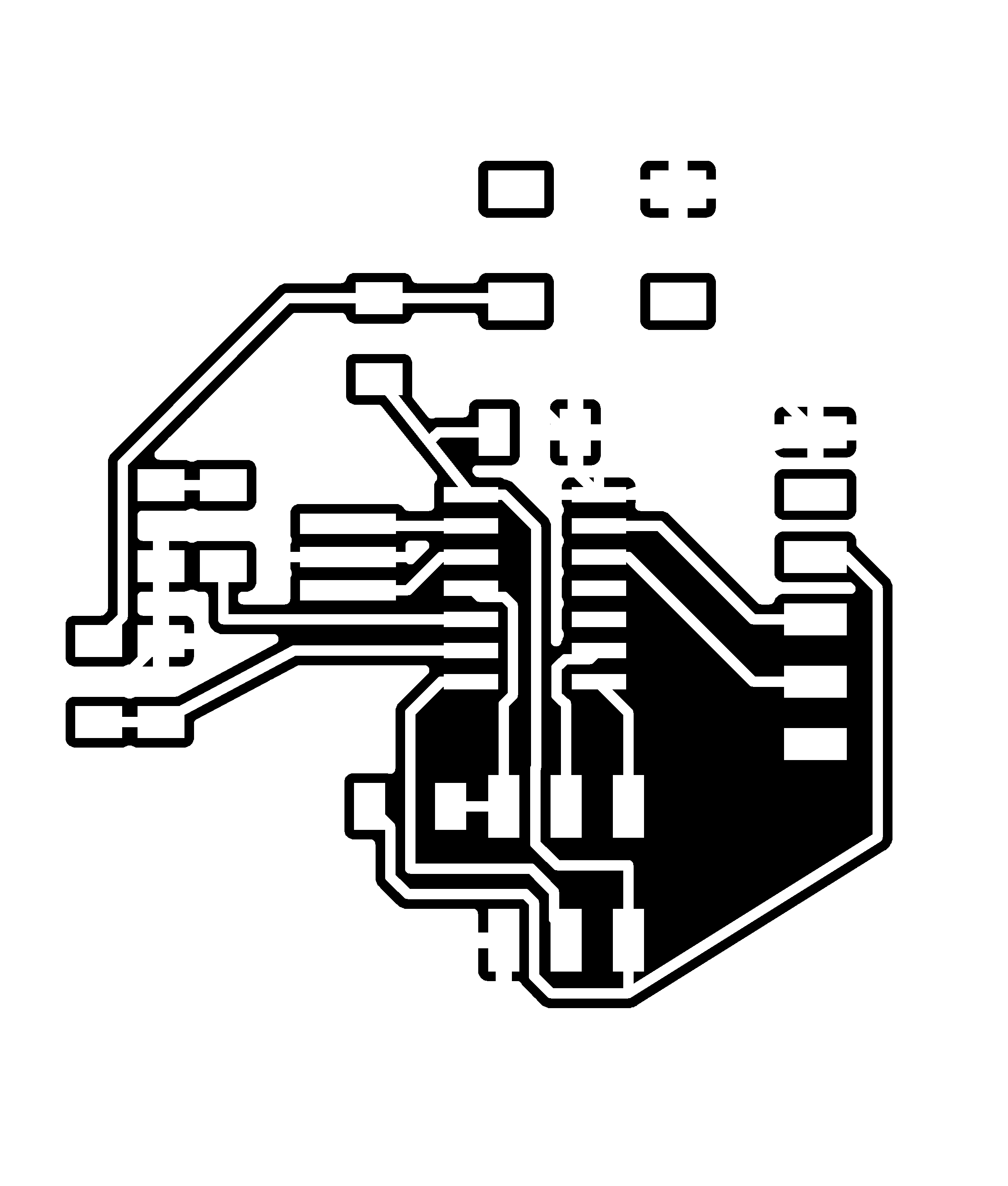
Traces and outline for the milling machine are presented below

png

png

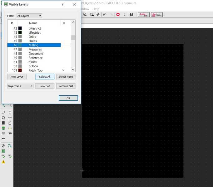
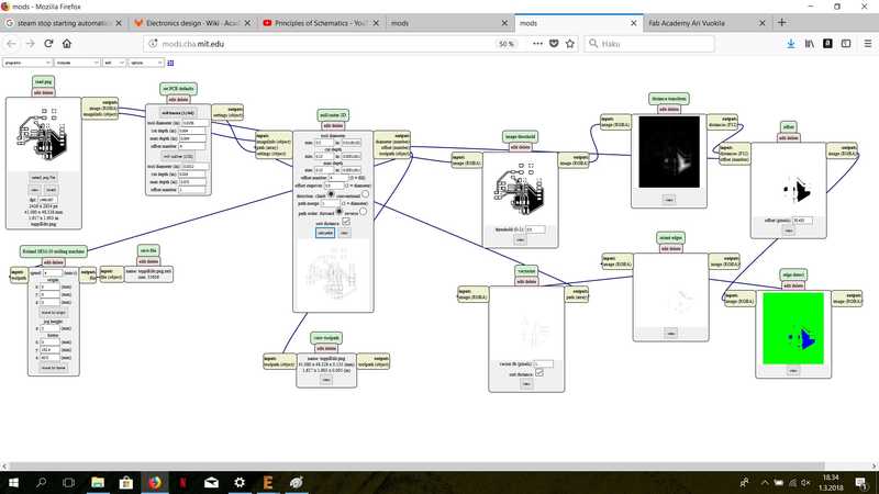
Mods was used to create rml files for the milling machine. In the mods, you begin by right-clicking the blank area and select programs -> open server program -> SRM-20 PCB. It opens the modules needed to create cut files for SRM-20 milling machine. Right-click on the white area once again and select (if mods is not used to control your milling machine directly) -> modules -> open server module -> save. Move the save module next to Roland SRM-20 milling machine module and remove WebSocket device (press delete in the module). Connect the outputs of the Roland SRM-20 milling machine module to the save module inputs. Then you select png file (for example traces) -> press mill traces (1/64) (set PCB defaults module), insert tool diameter (my case: 0.39 mm in mill raster 2D module), cut depth (my case: 0.11 mm in mill raster 2D module), max depth (my case: 0.11 mm in mill raster 2D module), change origin x, y, z = 0 mm in the Roland SRM-20 milling machine and press calculate in the mill raster 2D module. Now save file popup to your computer and check that all the toolpaths are correct with view toolpath module.

png

png
Milling process
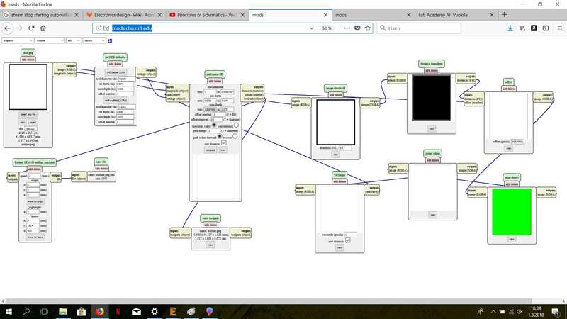
After the first milling was done, I realized that milling machine didn't do all the necessary lines and I had to remake the rml files, to correct the problem. Because the GND was set to all of the left over board, mods considered it as a wire and couldn't make the diagonal cuts based on the given settings. I changed the tool diameter from 0.4 mm to 0.3 mm and mods could create all lines and the milling machine as well. The milling machine and its use are presented in the Assignment 5.

png
Soldering the components
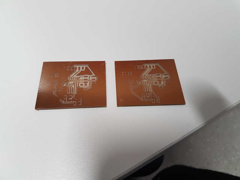
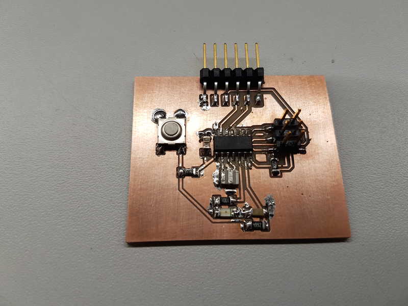
I collected all the components for the soldering, removed the surface layer from the board by scraping it with metal wool and worked in a similar manner to Assignment 5 i.e. I started from the hardest component ATtiny 44 and moved towards edges, which are easier to solder.

png

png
Programming the board
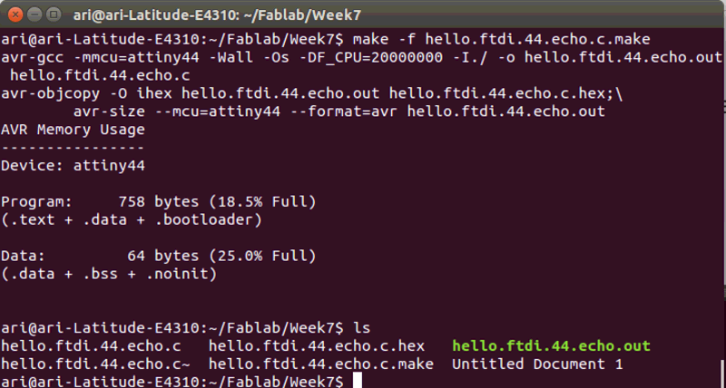
I downloaded the hello.ftdi.44.echo.c.make and hello.ftdi.44.echo.c files for the programming and testing of the board. At first, hex file is needed for the flashing. The command to create it is:
>make -f hello.ftdi.44.echo.c.make

png

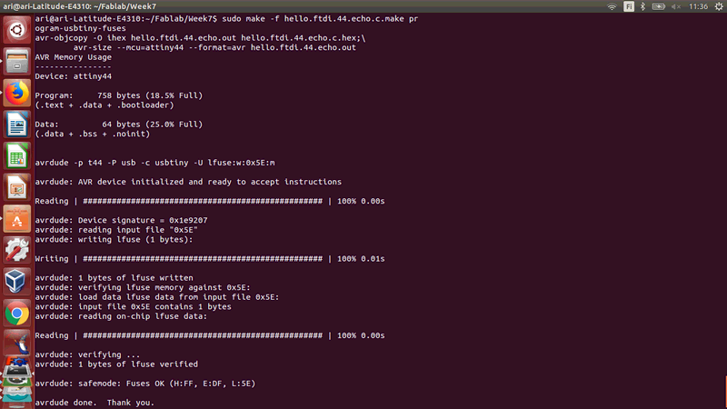
To make the microcontroller ready for programming run command
>sudo make -f hello.ftdi.44.echo.c.make program-usbtiny-fuses

png

To flash the microcontroller run command
>sudo make -f hello.ftdi.44.echo.c.make program-usbtiny

png

png
Testing the board
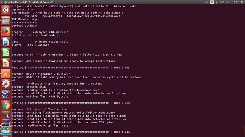
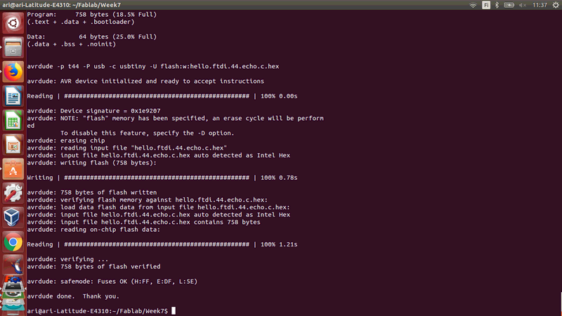
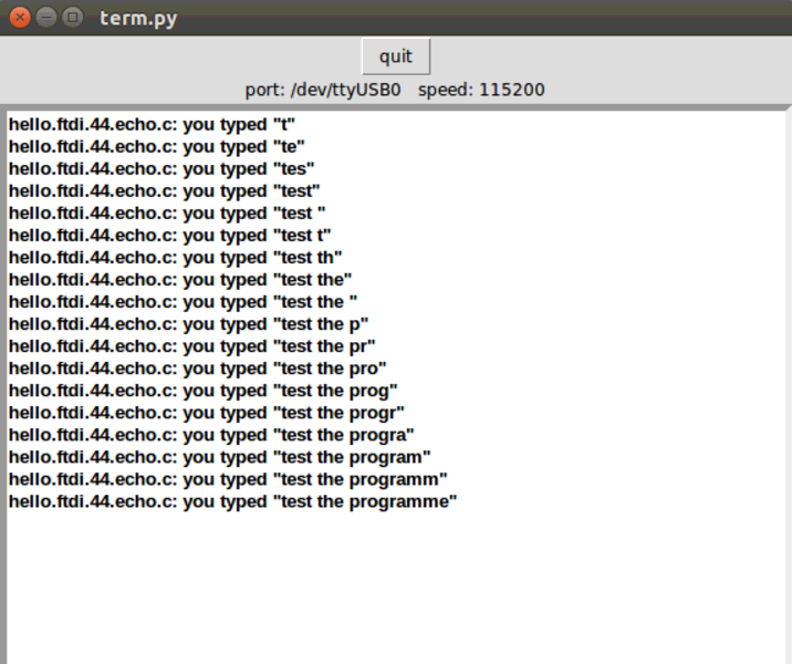
To test the board, I run an application with python. With this program, you access to your board and you simply press any key and the program will print the character.
>sudo python term.py /dev/ttyUSB0 115200
Everything worked as it should.

png
The files used in the assignment are shared below:
ElectronicsDesign.zip Files for the electronics design
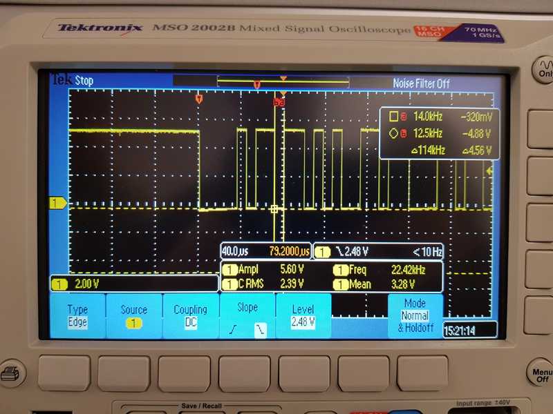
Group assignment

The group work consisted of using the test equipment in your lab to observe the operation of a microcontroller circuit board. The work is documented in our group page: Electronics design group page. We tested the board with a multimeter and an oscilloscope. We all tested our boards for short circuits with multimeter and we tested one board with an oscilloscope and we tested the button as well. We got nice signals from the oscilloscope and there were no short circuits in any of the boards.

oscilloscope