Assignment 09_embedded programing
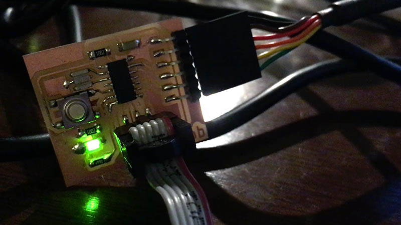
For this assignment, I remake both of my PCBs, the first one because the soldering was awful, and the second because I discover that were a problem with the file for the CNC machining, and a trace was missing (the one down the attiny44). So I remake both PCBs so that I could program them. You can check it in my Week 05 and Week 07 assignments.
01 read a microcontroller data sheet
I read the datasheet of the Attiny24A/44A/84A. It was a lot of information that was very good to understand where I can find it when I need to use a new component.
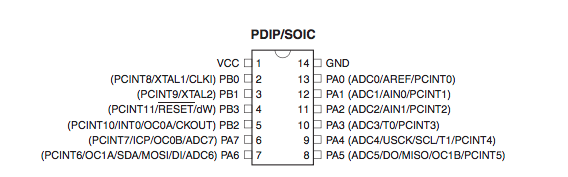
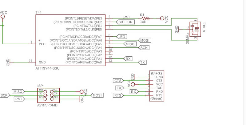
The first information you can find and is very useful is the detail of the pins of the microcontroller. I am going to use this a lot in the fab academy, for designing the boards and the write the code.
This was very useful for the part of my assignment where I work with the Arduino compiler ("ARDUINO IDE + ARDUINO COMPILER + AVR (ATTiny44))". I add the LED of my board in the pin PA7. In Arduino, I have to write like A7 or just 7
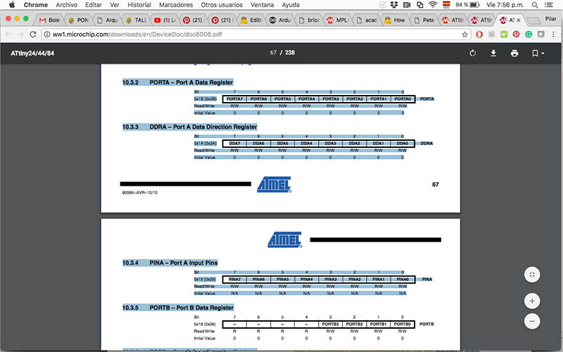
Also, the datasheet was very important to understand how to code in C for this assignment ("ECLIPSE IDE + C + AVR (ATTiny44)"). Because for that language you have to understand very well the possibilities and how to work with your microchip, specifically understand how the I/O Ports works (page 54). The physical I/O Registers and bit locations are listed in “Register Description” on page 67.
You can check the details of this below on the page, on the development of the assignment.
02 program your board to do something, with as many different programming languages and programming environments as possible
For this assignment I work with:
- Lenguajes:
- Arduino compiler
- C
- IDE:
- Arduino IDE
- Eclipse
I decide to use an elementary code just utilizing the led of the board so that I could try it on different architectures more easily.
ARDUINO IDE + ARDUINO COMPILER + AVR (ATTiny44)
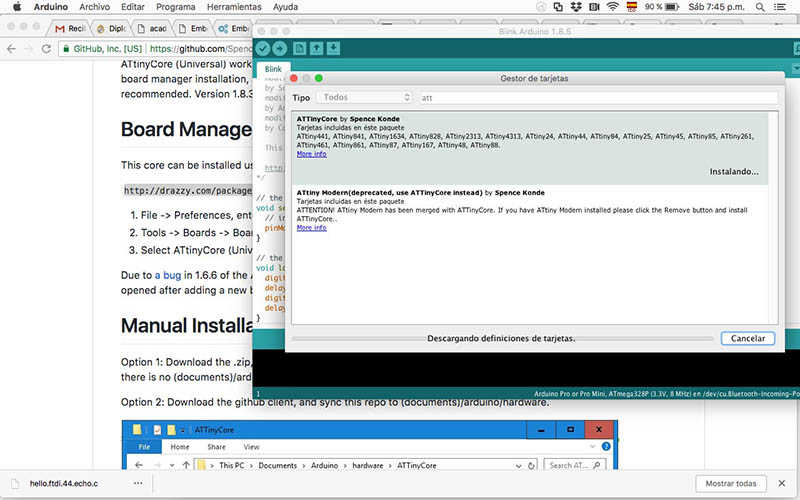
First, I add Arduino ATtinyCore and then add Arduino core for ESP8266 Wifi chipwith a driver. Now I can use my board and also my Wemos board that have an esp8266 chip
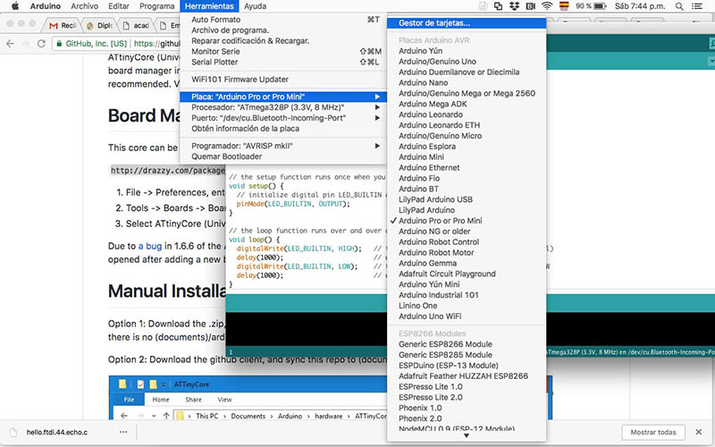
I check the ATTinyCore for review with was the name of the pin of my ATTiny44 on Arduino.
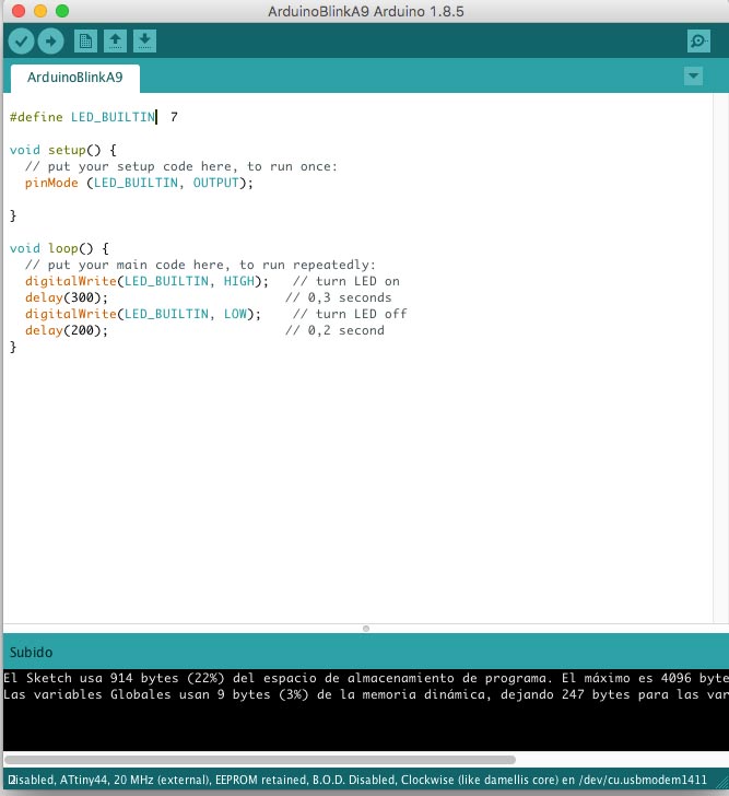
In my board, I have the LED in the pin PA7. In Arduino, I have to write like A7 or just 7.
The code I use was:
Fab Academy_BlinkArduino IDE from Pilar Bolumburu on Vimeo.
The code weight 914 bytes and use and 22% of the space. Work very well.

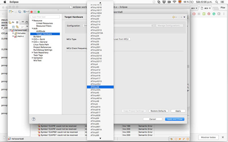
ECLIPSE IDE + C + AVR (ATTiny44)
I follow an Instructables tutorial to program my board with C in Eclipse.
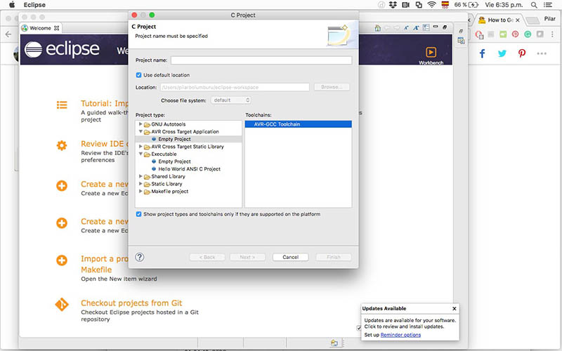
First I download Eclipse Installer, but when I was going to install the Eclipse for C I had some problems with Java actualization, so I have to update the package of Java Development Kit (JDK)
Then I download Eclipse for programming with C and Crosspack for setting up AVR. Trought Homebrew I install install avr-gcc. I also download a Plug In AVR on Eclipse.
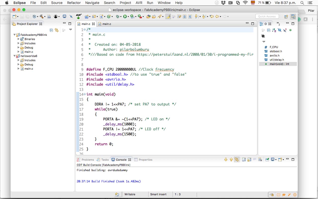
For creating the new project, I follow the Instructable tutorial. Use C code base from Peter Stuifzand website and change some of the definitions for making my blink code.
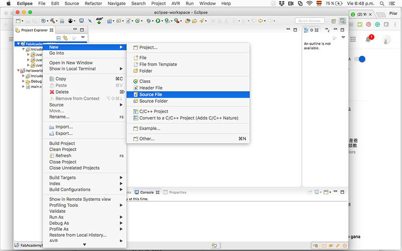
- So I create a new C proyect in the AVR Cross Target Application folder.
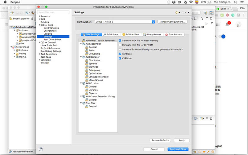
- I set Build Settings and choose which files and information I need it (Generate Hex File for Flash Memory, Print Size and AVR Dude).
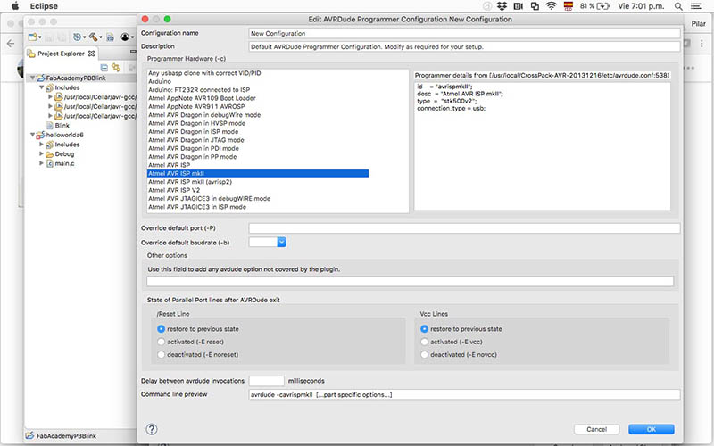
- Set AVR Target Settings > Select AVRDude > New > My programmer (Atmel AVR ISP mkll)
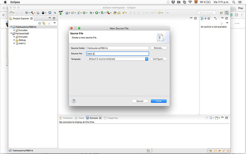
- Create new source file and name it "main.c".
- Set my clock and ATTiny44
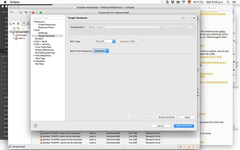
Once I copy the code of Peter Stuifzand, I change the clock frequency and add
#include
I also have to review again the datasheet of the Attiny24A/44A/84A for understanding how to work the pins of my microchip.
In my board, I have the LED in the pin PA7. I review in the datasheet the information about the I/O Ports (page 54), and the physical I/O Registers and bit locations listed in “Register Description” on page 67.
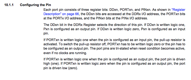
In the datasheet I read:
"The DDxn bit in the DDRx Register selects the direction of this pin. If DDxn is written logic one, Pxn is configured as an output pin. If DDxn is written logic zero, Pxn is configured as an input pin."
So, on my board, I was working with the LED that is an input, so the previous text should "translate" to my work as:
"If DDA7 bit in the DDRA Register, is written logic one, PA7 is configured as an output pin."
I also review the datasheet:
"If PORTxn is written logic one when the pin is configured as an output pin, the port pin is driven high (one). If PORTxn is written logic zero when the pin is configured as an output pin, the port pin is driven low (zero). "
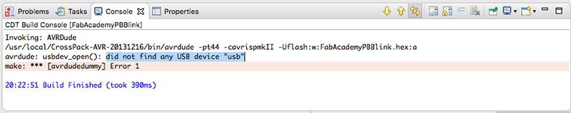
Once I had everything configured, I Build the project on my board, first remaining the LED on 1 second and then off 1,5 second. I had forgotten to plug the board, and Eclipse shows me the problem. But after that was everything ok.
Fab Academy_ Blink C lenguage 1 from Pilar Bolumburu on Vimeo.
Then I build another project with 0,2 second on and 0,3 seconds off. (download file).
Fab Academy_ Blink C lenguage 2 from Pilar Bolumburu on Vimeo.
Eclipse is faster on uploading the code to the board than the Arduino IDE. On the other hand, the C language is more difficult to start than Arduino but is more "connected" to what happens in the board. Arduino Compiler makes it easier, but you don't relate what you write in the code which how your board works.
03 compare the performance and development workflows for other architectures
ARDUINO IDE + ARDUINO COMPILER + ESP-8266
For compare, architectures of I review an article of Albert Heisenberg.
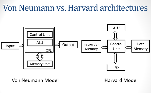
The main architectures are the Von Neumann and the Harvard architecture. Harvard architecture has separate data and instruction busses, allowing transfers to be performed simultaneously on both busses. A Von Neumann architecture has only one bus which is used for both data transfers, and instruction fetches, and therefore data transfers and instruction fetches must be scheduled - they cannot be performed at the same time.
In the same article, Lalit Tyagi comments the following characteristic of both architectures:
Von Neumann Architecture
- It is named after the mathematician and early computer scientist John Von Neumann.
- The computer has single storage system(memory) for storing data as well as program to be executed.
- A single set of address/data buses between CPU and memory.
- The processor needs two clock cycles to complete an instruction.
- Pipelining the instructions is not possible with this the first clock cycle the processor gets the instruction from memory and decodes it.
- In the next clock cycle, the required data is taken from memory. For each instruction, this cycle repeats and hence needs two cycles to complete an instruction.
- This is a relatively older architecture and was replaced by Harvard architecture.
Harvard Architecture
- The name is originated from "Harvard Mark I" a relay based old computer, which stored instruction on punched tape(24 bits wide) and data in electro-mechanical counters.
- The computer has two separate memories for storing data and program.
- Two sets of address/data buses between CPU and memory.
- The processor can complete instruction in one cycle if appropriate pipelining strategies are implemented.
- In the first stage of the pipeline, the instruction to be executed can be taken from the program. In the second stage of the pipeline, data is taken from the data memory using the decoded instruction or address.
- Most of the modern computing architectures are based on Harvard architecture. But the number of stages in the pipeline varies from system to system.

Este obra está bajo una licencia de Creative Commons Reconocimiento-NoComercial-CompartirIgual 4.0 Internacional.