
WEEKLY ASSIGNMENTS
Electronics Design
When you're talking about working outside your comfort zone … really this is it. This is the first time in my life working on something like this. The whole experience is WOW, learning and understand who thing run. Our instructor Sibu start with an idea about the task and what we need to cover, and he shows us an example, and recommendation how to start. I start reading a couple of articles about the electronics, the meaning of symbols.
I download the file and upload the library, start placing the symbols, testing the tools, and the setup for the components, Design Rules. The first test there were some issues regarding mix in naming links. After fixing it and other issues like (adding a connection point for the Button line).
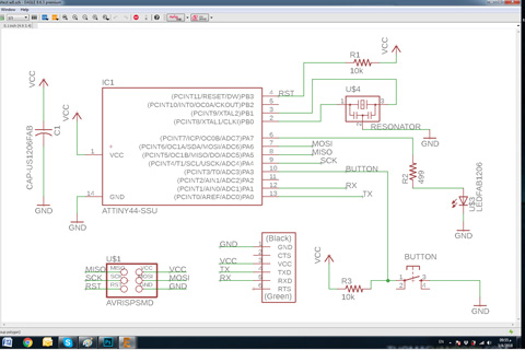
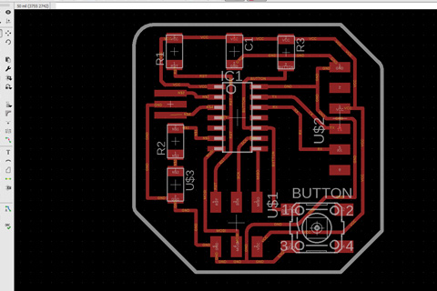
After finishing from the schematics I start with the board design layout
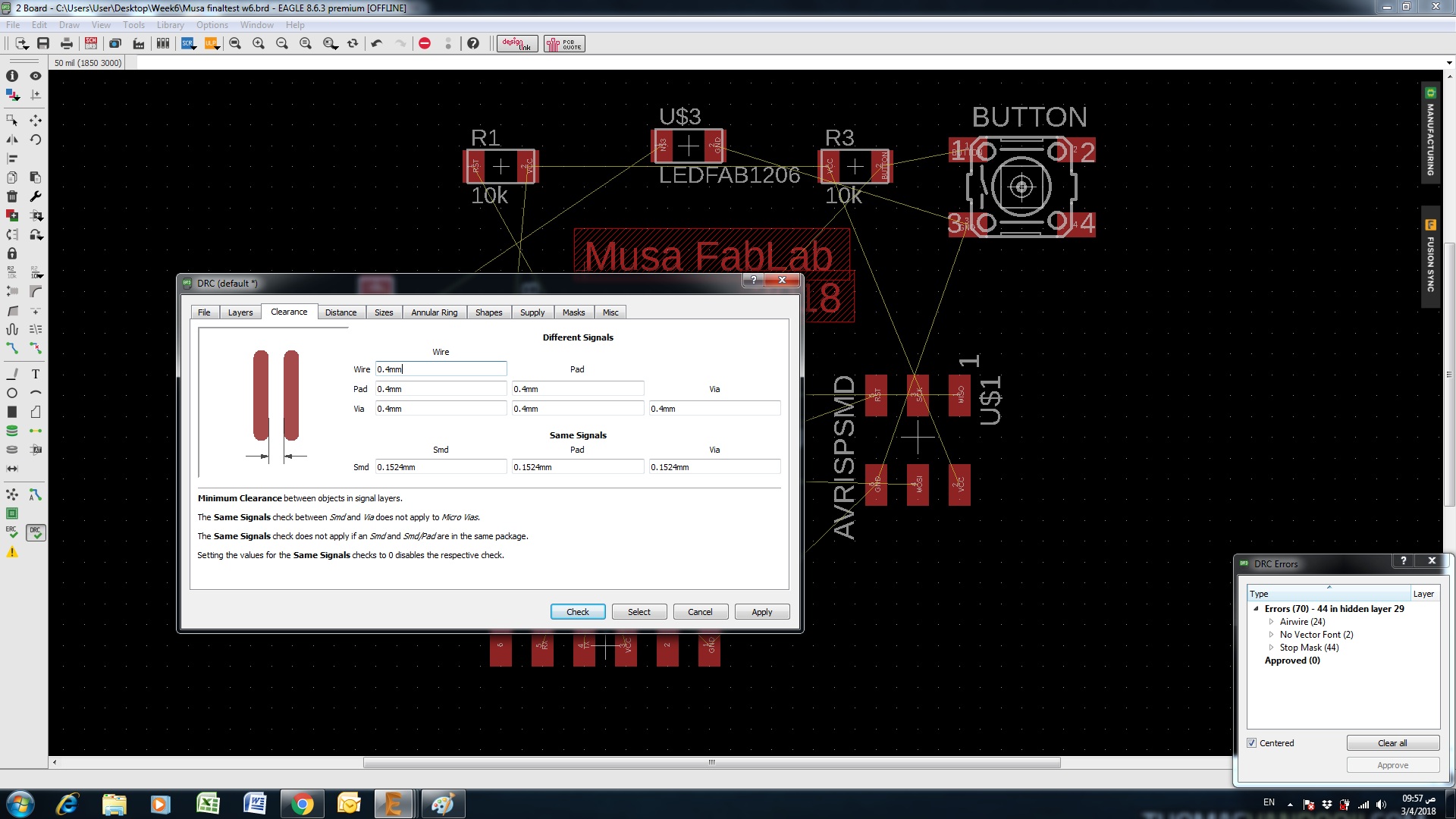
Design Rules
Clearance: Wire 0.4mm / Pad 0.4mm / Via 0.4mm
Size : Minimum Width 0.4mm / Minimum Drill 0.4mm
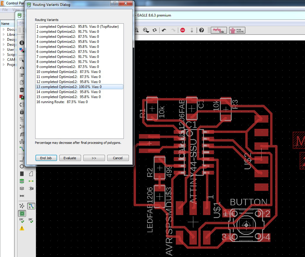
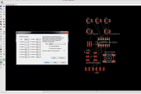
Working on the board design the layout, this was a bit forward and backward, coz you need to try too many layouts until you have the best links between components, it took me some time to finish this. Plus to make sure that there is clearance between the lines the whole setup needs to be super accurate. Each time I change the components layout I click on the RatsNest to see the new connection line ( green line ) to get the min from it, so when I run AutoRouter I am looking to get 100% as optimize. After that, I get to a point that is this best setup. then I start adding the Boarder for a board, by going to the layers and highlight option edge.
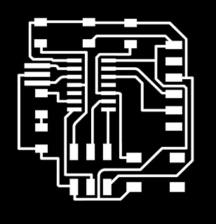
then Export ...Image .. for both the border and the circuit footprint resolution 2000DPI / monochrome using Photoshop I will up the black solid area in the border image as white.

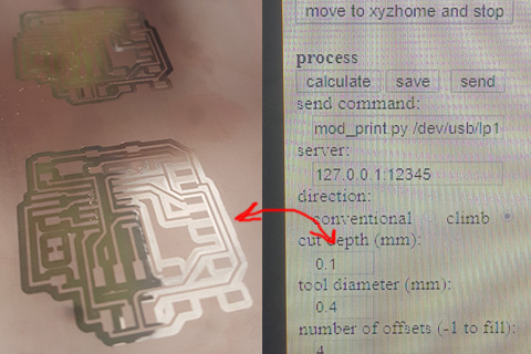
After I upload the images and set up the milling, the cut depth as 0.1mm, when it's dome I found out that only 50% from the board was milled, our instructor Sibu that the sheet has some bending so I need to increase the cut depth to 0.14mm. again only it milled 75% of the total. the 3rd time was ok and the cutting depth was 0.18mm
After all the milling I make sure that the board is clean and ready, collecting the components to start soldering. again it took me about 45 min to do this.
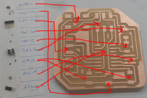
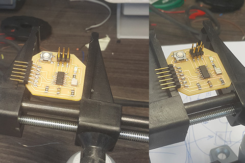
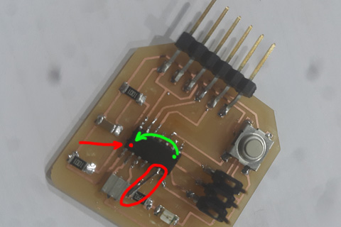
When I start programming. my friend notes that it is generating heat and that is a bad sign, so we start testing the links and the components, the ATtiny is flipped 180, I flip it ( green), during that I pull out some parts from the copper, we fix it by a soldering a wire between the 2 points ( red ), start programming we found out that it is burn. I print a new one start the process all over from milling to soldering.
the program did not work right, due to still I have some places the soldering wasn't good ( the legs for the ATtiny was not touching the board). fix them again, the program worked fine now. finally
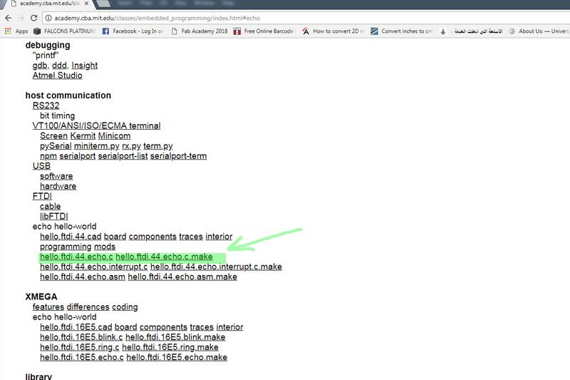
Download the make file and hello.fitdi.44.
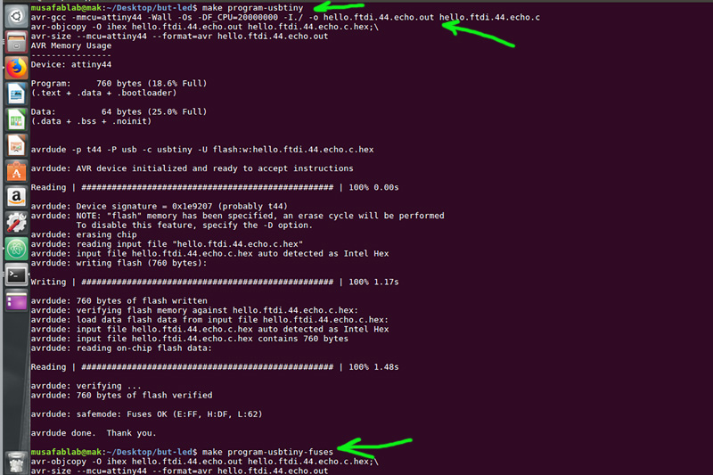
in the terminal run make program-usbtiny .... it will show you in the folder that generates a new doc ( name .hex) after it finishes 100 %. make program- usbtiny- fuses.All the above work fine then installing Arduino the device did not work again, testing the components, still, there were some issues regarding the soldering, fix them, retest work fine, link it to the computer and make sure it functions well ( sending an input the outcome is the same as input).
right click - save link as