Week 7
Electronics Design
This week's assignment was to observe the operation of a microcontroller circuit board using the test equipment at our lab, and to redraw the echo hello-world board in a PCB designing software by adding a button and LED. After checking the design rules in the software, the designed PCB has to be made and tested and its operation is to be simulated and measured.
PCB design process
Electronic design plays a major role in the functionality and the size and shape of the final project. A compact PCB will easily fit into the desired geomtery of the final device. The design has to take account of the capabilities of the milling machine and also the components available.
The process begins in the PCB Design software by creating a schematic drawing. The software has a library of different components from which we can know the properties of the component,both pysical and electronic. Adding the fab library to the software will make it easy to select the commonly used and available components.
The schematic drawing begins by adding the required components from the component library. The electrical connections between the components are then drawn by taking care of the junctions and the connections that cross over.
Using the software, the schematic drawing is then turned into a lay out of the components and the connections(traces) in the PCB. The components are to be appropriately placed and oriented so that the traces can be routed in the shortest way without conflict, making the entire PCB compact.
The design rules are then applied to the designed layout and then checked. The width needed for the traces, the clearance between the traces, component properties, and other layout constrains are specified and checked in this stage. While selecting the design rules, the capability of the milling machine also has to be taken care of. The clearence between traces need to be kept greater than the bit diameter.
After checking the design rules, a monocrome image of the PCB layout will be made in PNG format with seperate files for the traces and cut. The copper board is milled and cut in accordance with the image by using Fab Modules and Roland MDX-20. The components are then soldered onto the board to make the final PCB.
Working with Eagle
In Eagle software, the PCB design process begins in the schematc mode after which it is switched to the board mode. After installing Eagle, the fab component library was added. A new project was created in eagle inside which a new schematic was created. The first step is to add the components listed below.
1. ATTINY44-SSU (ATTINY44) (Package:SOIC14, Library: fab)
2. Resonator (Package:EFOBM, Library: fab)
3. Resistors - RES-US1206FAB (RES-US) (Package:R1206FAB, Library: fab).
Two resistors are of 10k and the thrid one is of 499 Ohm. Resistor R2 (499)
is used as the current limiting resistor for the LED and R3 (10k) is the pull up
resistor.
4. LED(Package:LED1206 , Library: fab)
5. MM_SWITCH6MM_SWITCH (6MM_SWITCH) (Package:6MM_SWITCH, Library: fab)
6. FTDI-SMD-HEADER (Package:1X06SMD, Library: fab)
7. PINHD-2X3-SMD (Package:2X03SMD, Library: fab)
8. CAP-UNPOLARIZEDFAB (CAP-UNPOLARIZED) (Package:C1206FAB, Library: fab)
The below image shows the schematic view after all the components were added and the electrical connections are made.
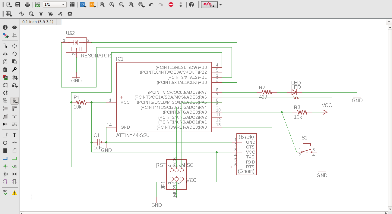
The schematic is then swtiched to "board view". The electrical connections drawn in the schematic will be preserved in the "board view" of Eagle. In the "Board view", the size and shape of the components will be visible, and we have to place each component in the proper orientation so that we can route the traces without conflict.
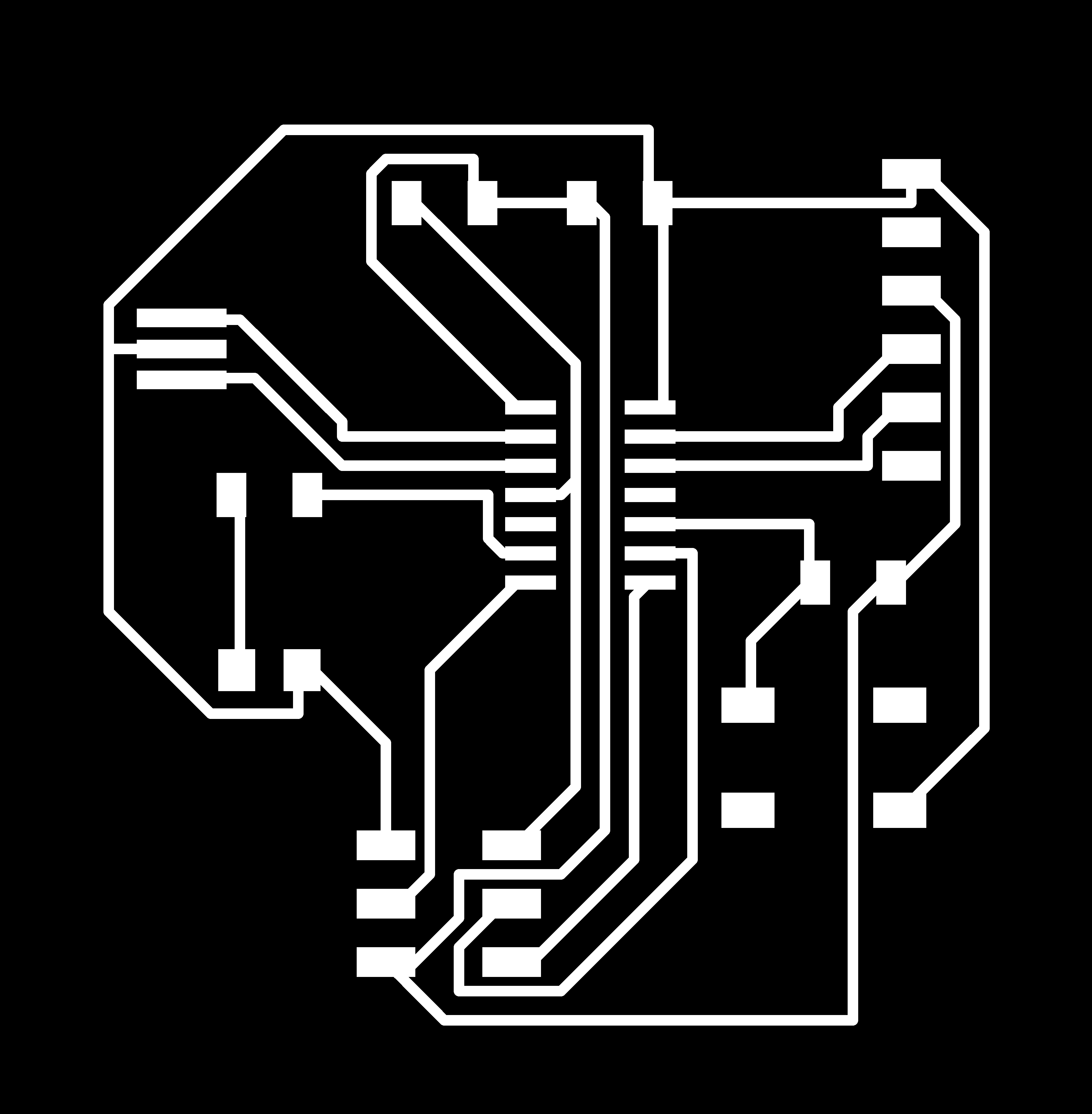
After switching onto board view, the traces have to be routed. The traces can be routed in two ways, manually and automatically. The traces can be drawn manually by selecting the "route" option in Eagle software and drawing the traces manually. The auto router feature under "tools" menu when selected will make the software to show possible trace routes from which we can select the best one. In my case, the software displayed a route which had 100% electrical connection. I chose the software suggested autoroute to fix the layout of components and traces. The below image shows the layout of the components and the traces.
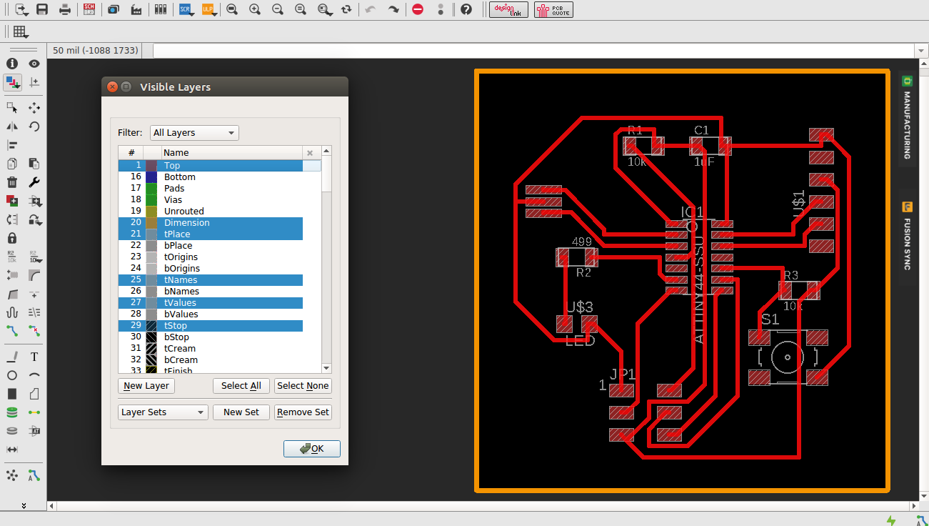
If the position and orientation of the component is such that there will be conflict between the traces, the software will not display 100% when the autorouter is selected. In that case, the conflicting connection will be shown in yellow lines, and we have to route that trace manually or by selecting autorouter feature after changing the orientation and placement of the components to accomodate every trace without conflict.
Making of the entire electrical connection in the schematic by drawing wires will become messy when the circuit is big. An easier way to make the electrical connection without the wire is to provide a NET to the component's and then Naming (and Labeling) the respective NET which are to be connected with the same Name.
After making the traces route, the next step is to check the design rules. The "design rules" option is available under the "edit" menu of Eagle, where in we can specify each of the parameters of our design. The below image shows the values that were used for the design rules which were also the default values.
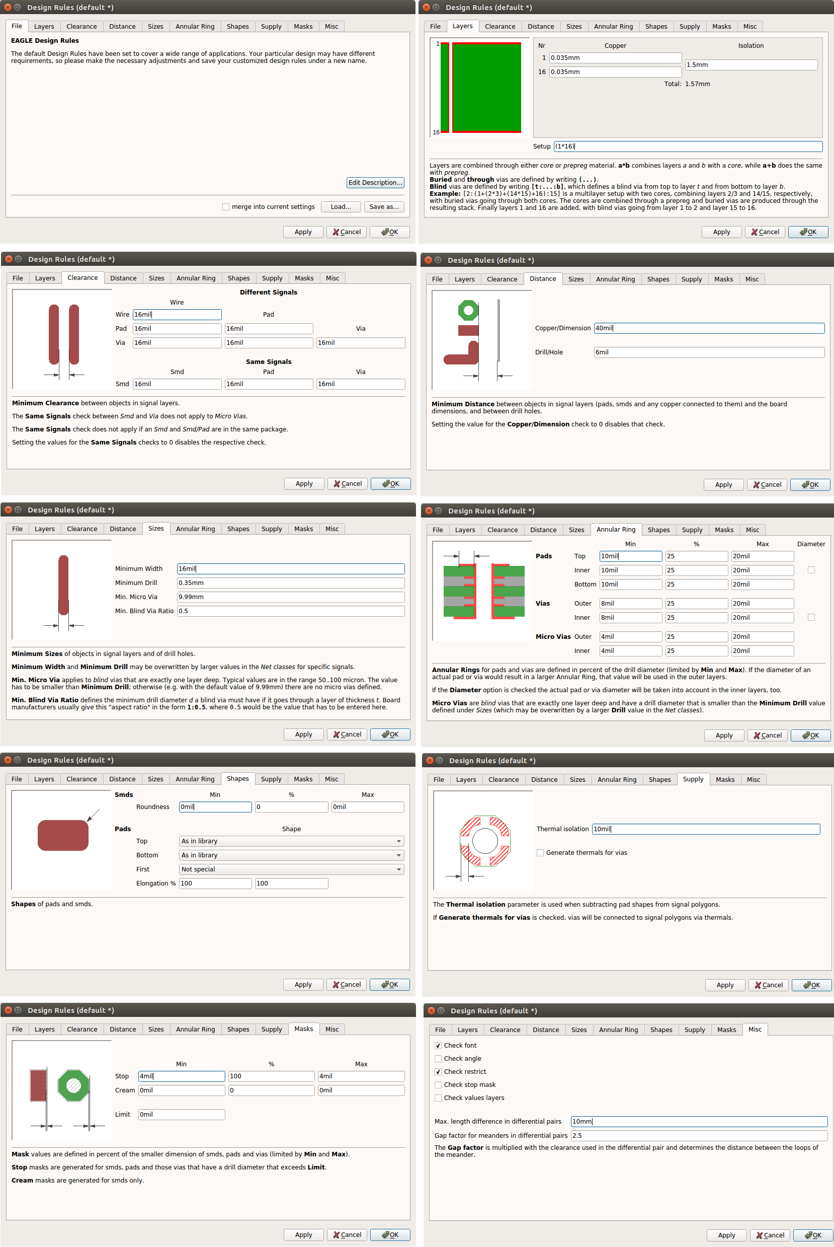
The next step is to check the design rules. The same can be done by selecting "DRC" option available under "tools" menu. The design check should return a zero error for proceeding further. If any errors are displayed, the same has to be rectified manually. One of the common error is insufficient clearence between the traces.
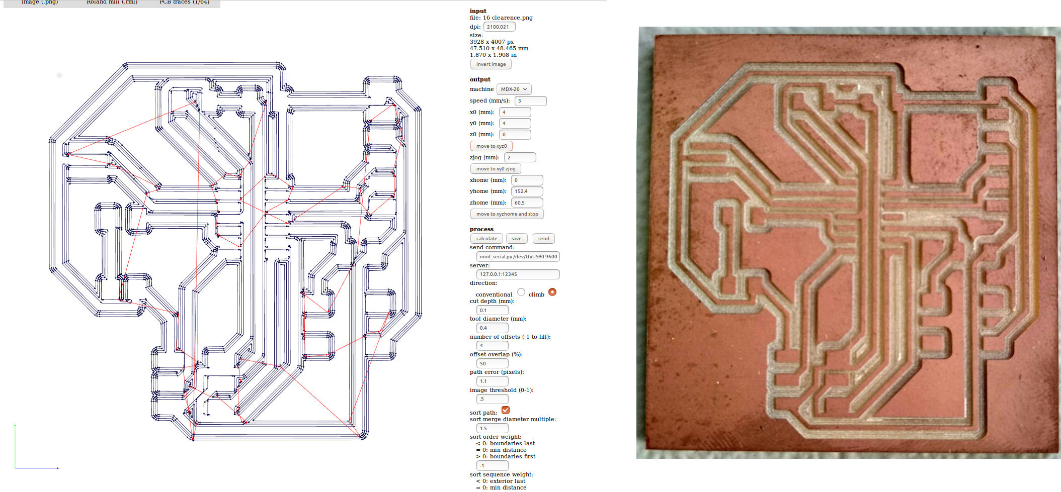
Once the design rules are checked and is free of any error's, we are set to mill the designed board. We need monochrome PNG images for the "traces" and the "cut". For getting the PNG image for "cut", we need to draw a boundary for our designed board and appropriate width has to be given by editing the properties of each of the boundary lines. (The property window can be opened up by right clicking over the boundary line and by selecting properties). The design can be directly exported to PNG formate in Eagle. By turning on only the visibility of "top" layer in Eagle, we can isolate the traces. After doing so, the PNG image can be exported by clciking on "file" menu. The image should be exported in monochrome with high resolution. For getting the PNG image for the cut, we need to make visible only the "dimension" layer in Eagle and the file for the "cut" can be exported.
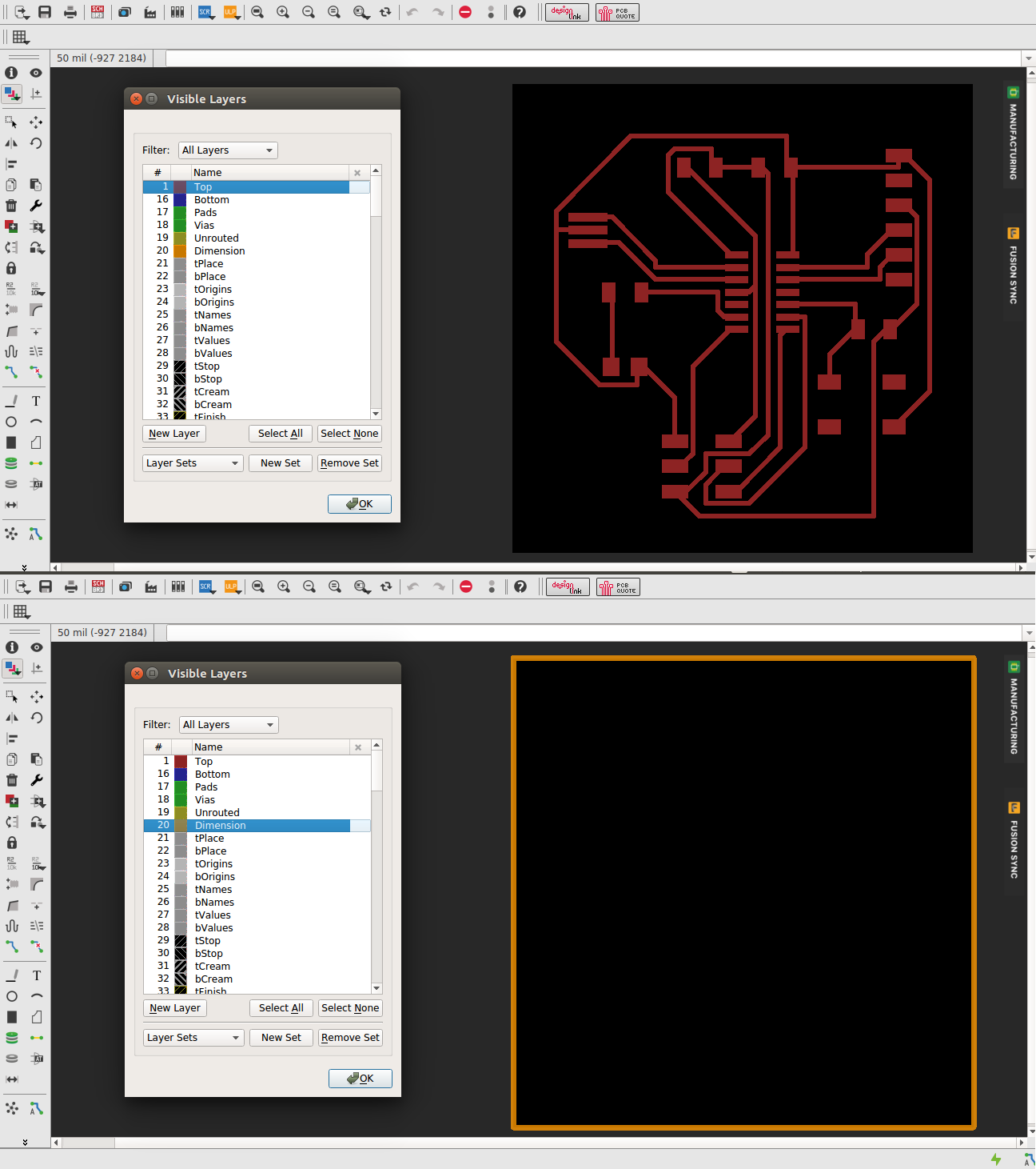 Below is the PNG files exported from Eagle software with which the board was milled
and cut in the Roland MDX-20. More details on PCB production can be
found at the Electronics Production Week's page.
Below is the PNG files exported from Eagle software with which the board was milled
and cut in the Roland MDX-20. More details on PCB production can be
found at the Electronics Production Week's page.

Click here to download the design files
Production & Testing
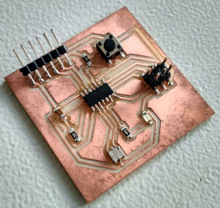
The board was milled and cut and the components were then soldered in the correct orientation.Below is the image of the final PCB.
The next step was to program the micro controller by connecting the board to the ISP made during Week 5. After connecting the PCB to the ISP, the ISP is then connected to the computer to flash the programme. The programme in C (hello.ftdi.44.echo.c) and the make file (hello.ftdi.44.echo.c.make) was downloaded from the Fab Academy Website.
After downloading the files, rename the hello.ftdi.44.echo.c.make file to Makefile. After doing the same, open up the terminal within the directory where the files are downloaded and following commands were entered one after the other to flash the program into the microcontroller.
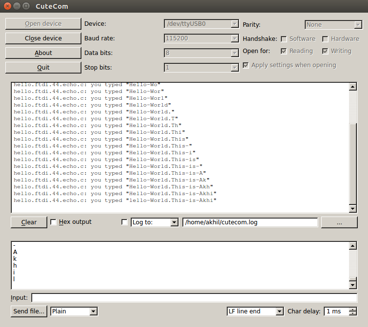
makemake program-usbtiny-fusesmake program-usbtinyThe next step is to test the PCB. To do the same cutecome was installed and the board was connected to the laptop through FTDI cable. The board was echoing what was send in the serial window.
Errors Committed
When the traces image was imported into fab modules, the tool path displayed was not correct with the tool skipping two paths on the ISP header. This was left unnoticed before the milling operation and was discovered only after the operation was completed. The copper at the two uncut portions were manually cut before the soldering operation. The error happened due to the insufficient clearence specified in the design rule.
Electronic Design for the Final Project
Electronic Design for Input Devices week
Electronic Design for Output Devices week
It is always advicable to use the manual routing of traces, for the autorouter feature in EAGLE will make things messy when there are more number of traces. Add each component in the schematic, make the electrical connections, then switch over to board to place the components, and then manually route the traces. In the event of unavoidable conflicting traces, use a zero ohm resistor to bridge over the trace.