Week 7: Electronics Design
Group assignment: use the test equipment in your lab to observe the operation of a microcontroller circuit board
Individual assignment: redraw the echo hello-world board, add (at least) a button and LED (with current-limiting resistor) check the design rules, make it, and test it
Individual Project
This week assignment is to make an echo hello-world board and add a button and LED to it. Default hello world board contain only Pullup- Resistor, Capacitor and Attiny 44, along with that we need to add a LED and Button Switch to make a new one. Attiny have an internal Clock of 8 MHz, for better use we need to add an external clock, here we choose 20MHz resonator ( While adding an external clock we need to put two capacitors and ground it but for Resonator it already has the same )
Below informations are from these pages : webpage 1 webpage 2
Pullup-Pulldown Resistors
In digital circuits which have Logic gates and IC, they have pins for input and output, and these inputs and outputs need to be correctly set, either HIGH or LOW for the correct working of circuits. Using Pull-up Resistors and Pull-down Resistors to give the input pin or output pin a defined default state, even if the switch is open, closed or there is nothing is connected to it..
Pull-up resistors are resistors which are used to ensure that the input of the IC is pulled to a high logical level in the absence of an input signal.
Pull-down resistors work in the same manner as pull-up resistors, except that they pull the pin to a logical low value.
Resonator( Details taken from this source)
A resonator is an electronic component consisting of a piece of a piezoelectric ceramic material with two or more metal electrodes attached. When connected to an electronic oscillator circuit, resonant mechanical vibrations in the device generate an oscillating signal of a specific frequency.
PCB Designing
We need to redraw the Hello Echo board and add an LED with a current limiting resistor and a Switch. Additionally we have to mill and stuff the board and see if it is working. In order to redraw I used Eagle software. EAGLE is a electronic design automation application with schematic capture, PCB layout, auto-router and computer-aided manufacturing features.
Eagle PCB Designing
I need to make a single sided PCB, First I downloaded Eagle software from there website, and then install it.
In order to design a PCB, you need to complete the following steps:
- Create a schematic sheet & add components
- Add nets to the schematic (connect components)
- Check schematic (Electrical Rule Check or ERC)
- Create a board outline
- Position components on the board
- Route tracks between the components
- Check board (Design Rule Check or DRC)
- Perform Final Checks
In EAGLE the schematic design takes most of the time, this is the first time I was using different software for pcb designing. I was much familiar with Proteus Software; Now I think it's better to study a new one it should be great.
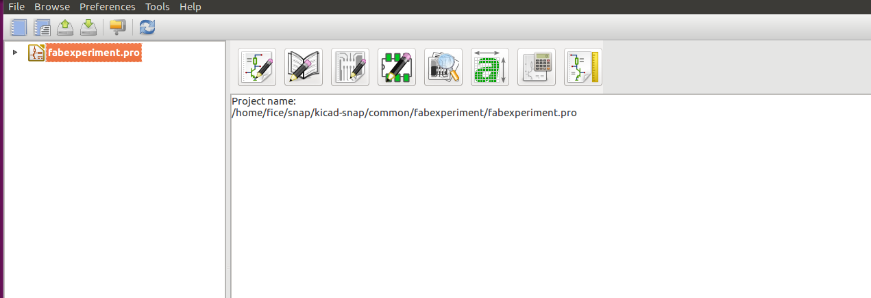
Open the Eagle software and click on File -->New -> Project , and give a project name Fabexperiment . Then right-click on that and New-> Schematic , a new window will open up then I save that as amith.sch
Familiarize with Schematic Section
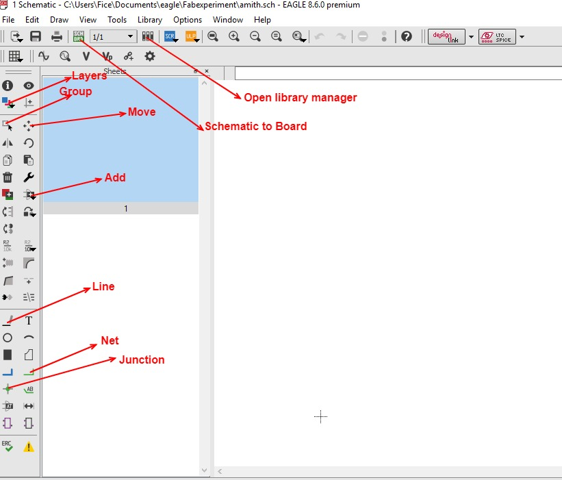
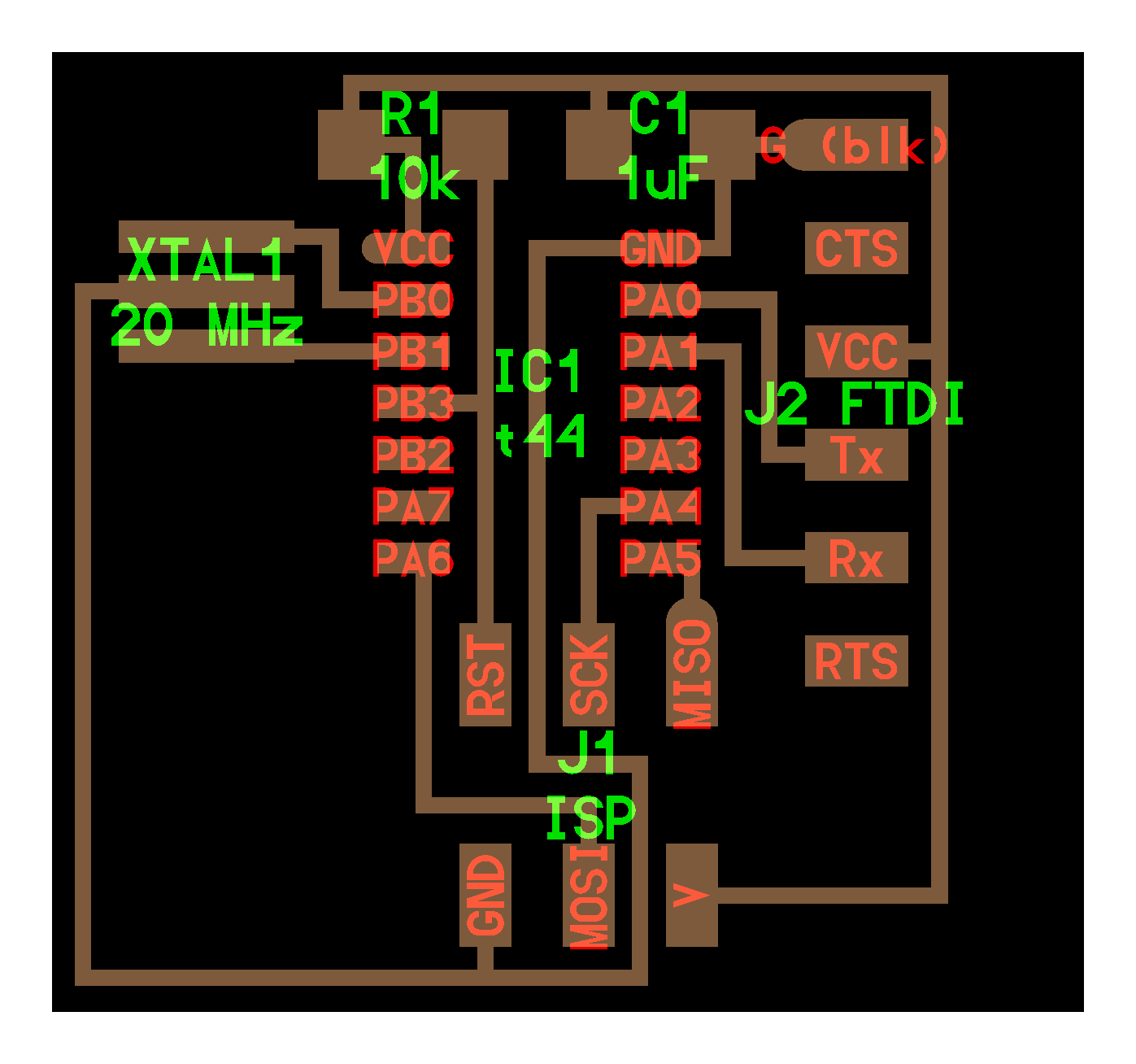
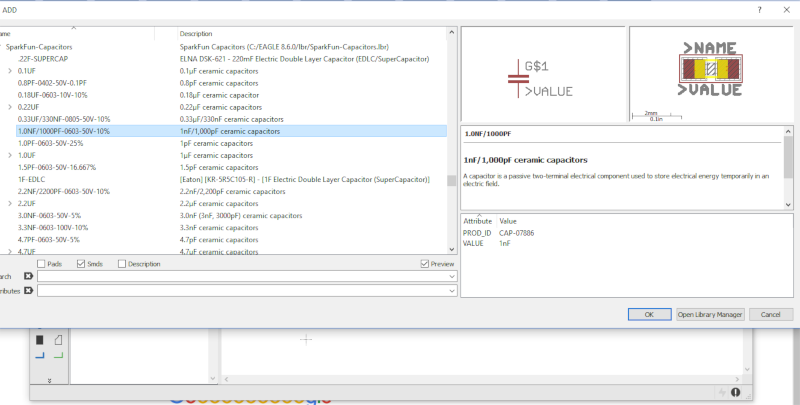
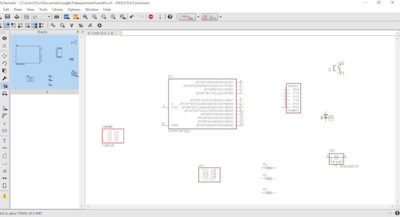
Now we need to draw the schematics by referring the above image. We need to add components using add button, but searching inside the component library, I can't find the parts so I, need to add the Library of components that I need to use. Fab itself provides a library for all components used during the fab academy, so I download that files from here and extract and place that in a \eagle\lbr folder which eagle installed.
Add components to your schematic click on Add then a New window which contains a list of components Some components have multiple packages ( select the correct package). The component schematic symbol and package layout appear in the two windows to the right of the library window. Each component has a description you can check to see what it is. When you have identified the correct component and package (component & package will be visible in the two windows), click OK to start the ADD procedure
Add all the components using this setup, components can also be moved after adding, with the click on Move and click on + sign( select the component) or rotated with the click on Rotate and click on + sign( select the component)
Using Group we can operate on many components at once - to move them.
After Placing all the components Click on Line and connect the components. The connection will be made and highlighted green with connected wires
Supply connectors : Supply connectors are a special type of component which does not exist physically on the PCB.
Where a wire joins the middle of another there must be a green circle (Select Junction and click on the point to make it) to indicate connection. While designing schematics I add normal header pin to unused pins of microcontroller for later use.
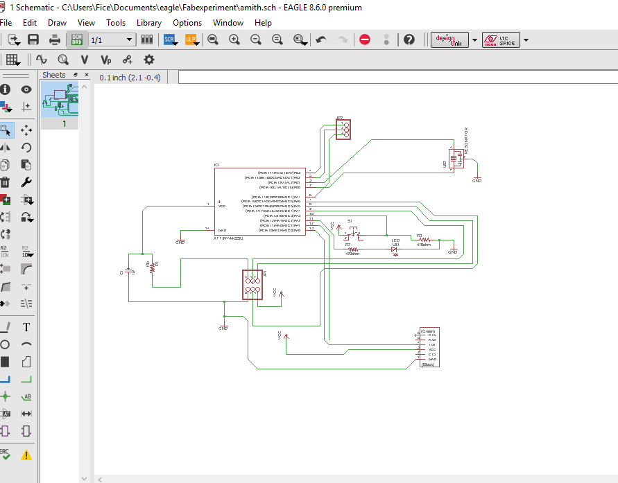
After completing schematics check the ERC and no errors are detected and the Select the Switch to board button opens the new window for designing the Board
Board Creation & Layout
File->Switch to Board or Click on the Switch to board button ,Since the schematic does not yet have a board attached you will be asked whether you want to create one from the schematic: say yes.
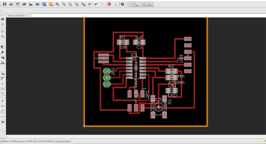
Initial schematic components outside the PCB outline, with Orange colour . Note the cross indicating (0,0). Select the components and place it inside the PCB outline.
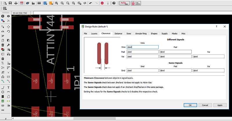
In order to draw the traces and pad , first we need to changing the default DRC rules for that we open
Eagle design rules by Tools -> DRC
First we need to change the clearance to 16mill by default 6mill
Second we need to change the distance where copper dimension is set as 40 mil
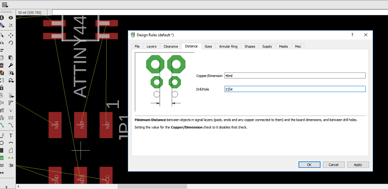
Then we need to change the size , where minimum width is set to 20mil by default 6mill is present ( choose depends on the tool bit used for tracing)
After setting we need to Route the track Tools -> Auto router
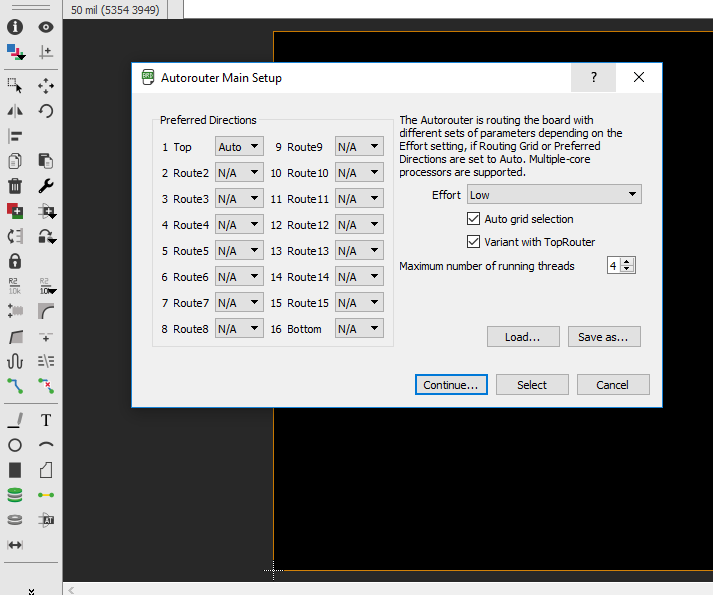
In Preferred Directions set Top as Auto and others as N/A, Set effort as high and Number of tread as 4. After that click on ok then start auto route. By know the routing is complete because of the message in the bottom edge of the window. Anything less than 100% indicates some connections not routed. But i choose manual routing .
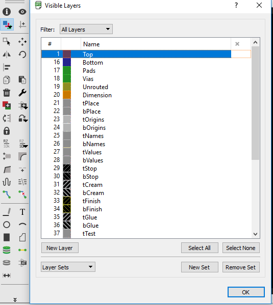
After Routing that I export the file as Image . Before that, I select the top layer, because I only need the traces. After that select monochrome and give a resolution of 600 then export.
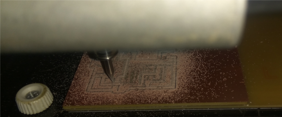
After exporting the PNG files for trace and dimension from egale software, i just copied these to computer connected to Modella MDX 20 .First i load the traces PNg and select outpurt format as Rolland Mill.rml and process as pcb traces 1/64.Make other as By default and Made that
After performing the Milling purpose, I go to inventory section and select the components ,
List of components.
- Microcontroller:- Attiny 44
- 2/4 pin tactile switch
- Resistors :- 10K-2nos,, 490 Ohm,
- 20Mhz crystal oscillator
- Capacitor 1uf -1no/li>
- Red LED -1nos
- 2x3 header pin
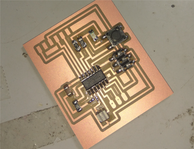
After selecting all components I just solder all things except SIL horizontal male pins , which are costly and not easily available.I need to replaced by straight male header pins.before soldering that I need to check my board is ready for communication
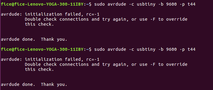
The Attiny44 microcontroller communication can be checked using FabISP. The following command is used to check the communication.
sudo avrdude -c usbtiny -b 9600 -p t44
avrdude is the driver for Atmel microcontrollers, -c option is for specifying the programmer followed by its name, here its FabISP. -b option is the baud rate followed by the speed. -p option identifies the device to which the programmer is attached. t44 is for Attiny44
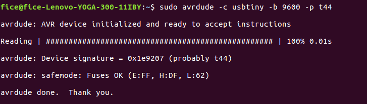
The output from the above command shows that board not communicated, I realise there must be some mistake occur while designing my board. So I check the continuity of board and realise that Attiny 44 does not get VCC, so I check the schematic that I miss two things.
- VCC connection to Attiny 44
- PB3 must be connect to RST
So I used 2 Jumper wire to make it correct. Then once again I used the above command and it detects, my board is now good for working.
After that I Solder the Header pins for serial communication, We are lack of headpins of SMD type, so I used Normal header pin for Soldering that but its difficult to make it, after working some time I fix that to my baord
Now we need to program Attiny 44, i have a FT32 TTl converter , here in which TX pin from attiny connect to TX pin and RX pin of attiny connected to RX Pin of TTl Connector, Connect VCC and GND of TTl with respective pin in Attiny board i made.
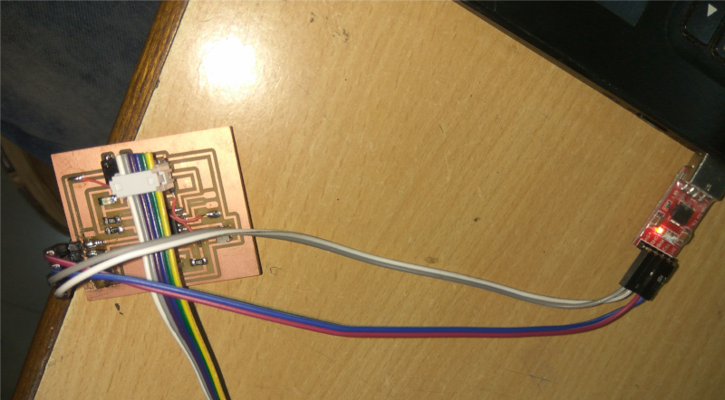
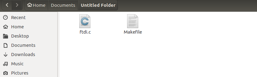
After Connecting i just open the Arduino IDE and check on ttols My board is detected as ttyUSB0. Files for compiling is download echo programand Make file After download these files , hello.ftdi.44.echo.c save as ftdi.c andhello.ftdi.44.echo.c.make as make, and open make file and rename hello.ftdi.44.echo as ftdi.
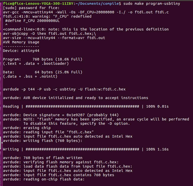
Open the Folder in Terminal by Right Click and Open it terminal and then type the following Commands
sudo make program-usbtiny
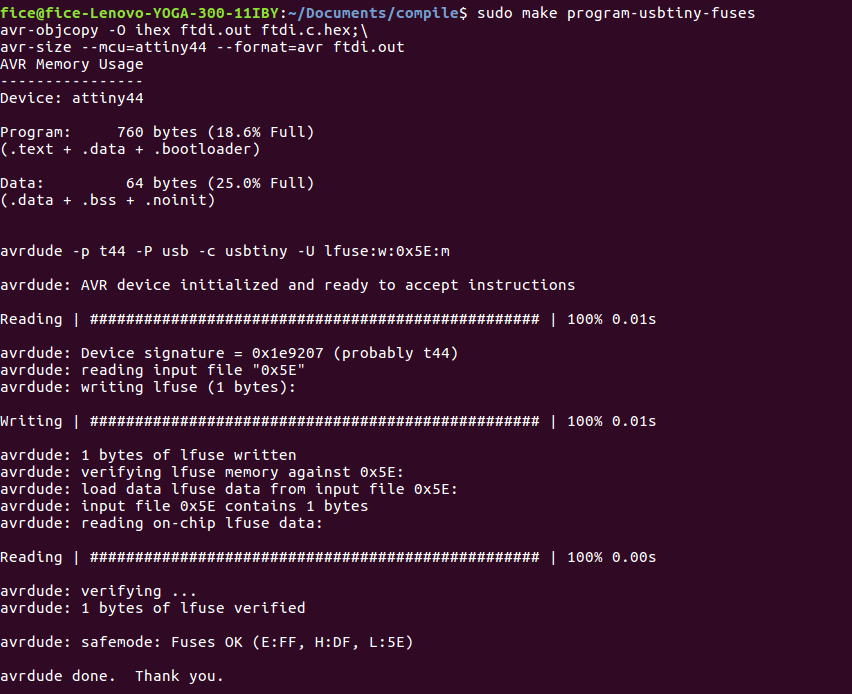
sudo make program-usbtiny-fuses
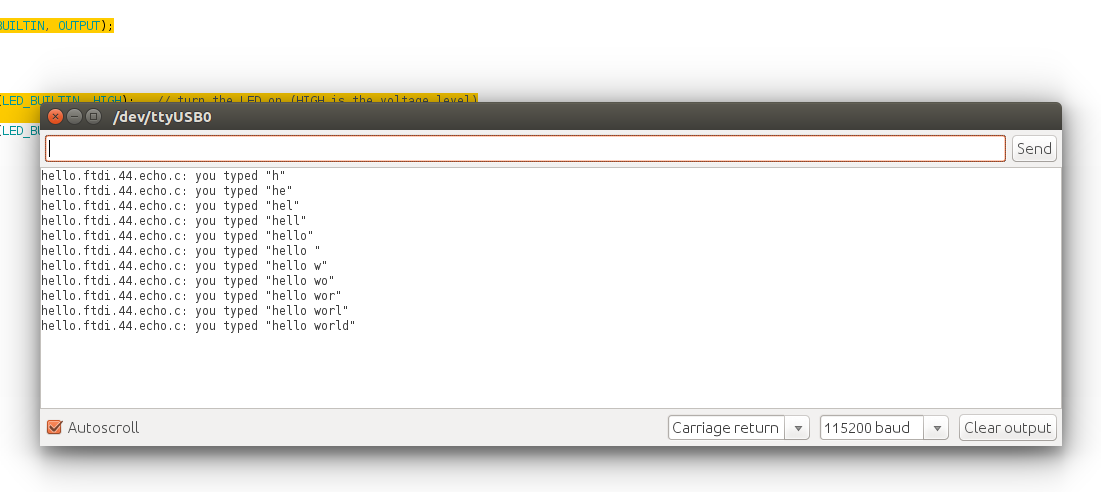
After that open the serial monitor in Arduino IDE and Set baud Rate to 115200, Carrigae return and Type characters and send over serial monitor, As I am getting the expected result, The board is working fine.
PCB Design with KiCad
KiCad is an open-source software tool for the creation of electronic schematic diagrams and PCB artwork. Before start, I need to install KiCad in my system, using ubuntu software center I install KiCad. After Installation Open KiCad and Create a New project. File → New Project → New Project, . The project file will automatically take the extension ”.pro”. KiCad prompts to create a dedicated directory.Details are copied from Kicad website Link
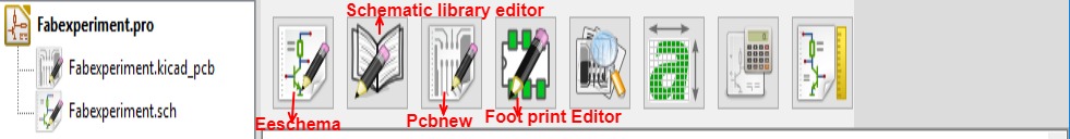
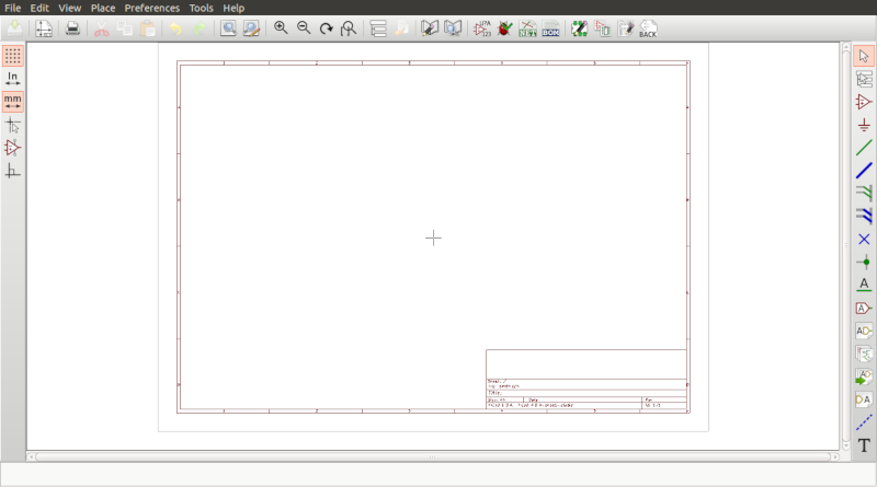
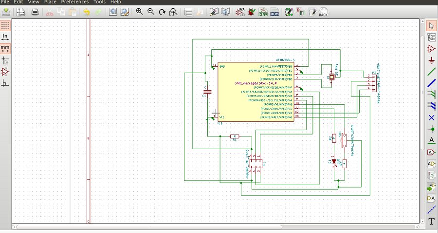
Creating a schematic. Start the schematic editor Eeschema, . It is the first button from the left. Click on that it will open a window ,here in which we draw the schematics
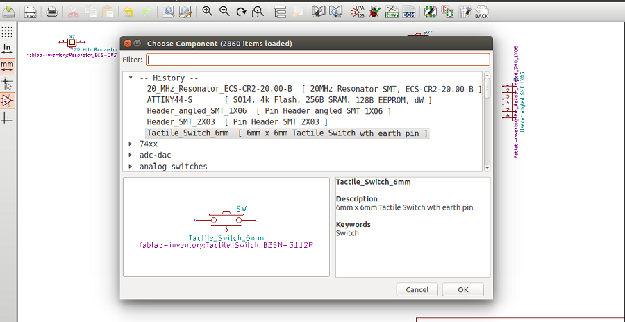
Now I am going to add a component from a library that isn’t configured in KiCad, Kicad Libraries can be download from here . In the menu, choose Preferences → Component Libraries and click the Add button for Component library files.
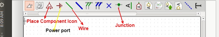
Place the components using component place tool and Use wire tool to make connections, Use “m” for move and “r” for rotate the components.
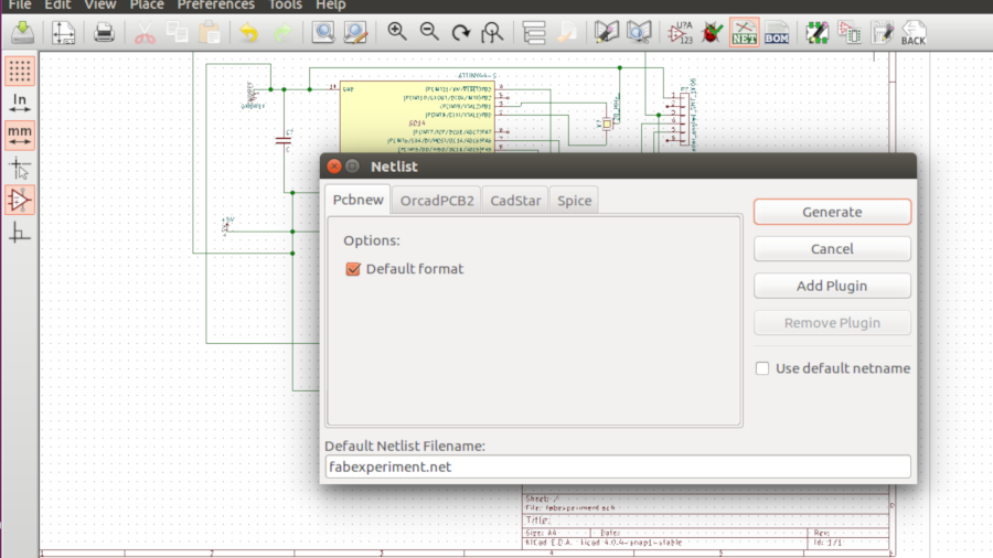
After Draw the schematics, click 'generate net list' icon and save.,
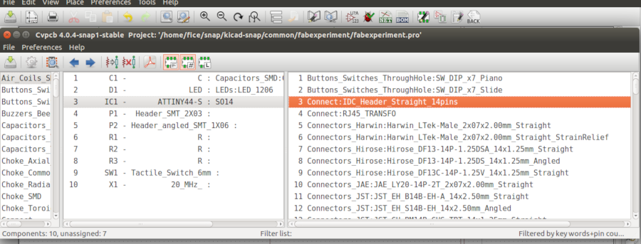
Now i need to assign components to the schematic. Run CvPCB icon, and add the SMD components. Generally, 1206 code used for SMD components. After selecting all components click 'generate netlist' and save. Every time you need to repeat this if you alter your schematic. Electrical rule check (ERC):- You can perform an electrical rule check by clicking the ERC icon. This program will check for missing connections, junctions, power supply errors etc.
Design PCB
After Complete Schematics click on the Pcbnew icon. The Pcbnew window will open. I start by setting the clearance and the minimum track width . In general you can set the clearance to 0.25 and the minimum track width to 0.25. Click on the Design Rules → Design Rules menu I have opted 0.5 mm track width.
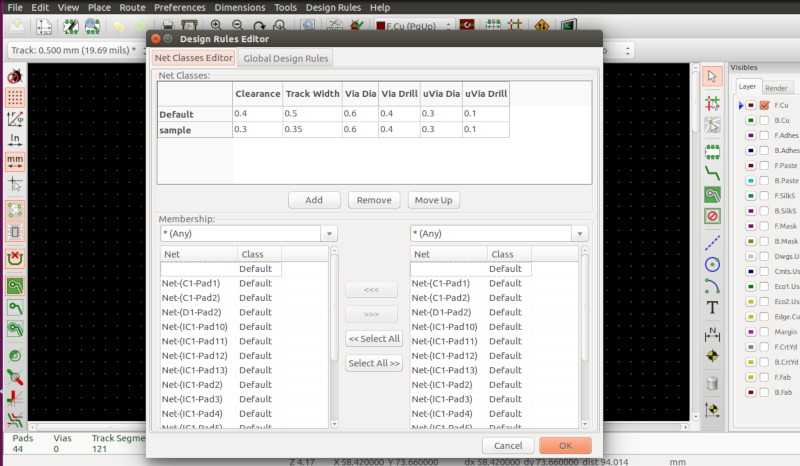
Click on the Global Design Rules tab and set Min track width to 0.25’.
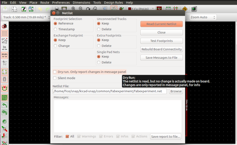
Now I import the netlist file. Click on the Read Netlist icon on the top toolbar. Click on the Browse Netlist Files button, e, and click on Read Current Netlist. Then click the Close button. All components should now be visible in the top left-hand corner just above the page select all components with the mouse and move them to the middle of the board. If necessary, you can zoom in and out while you move the components.
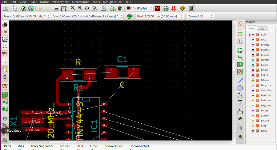
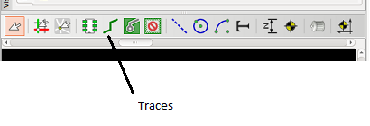
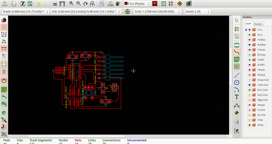
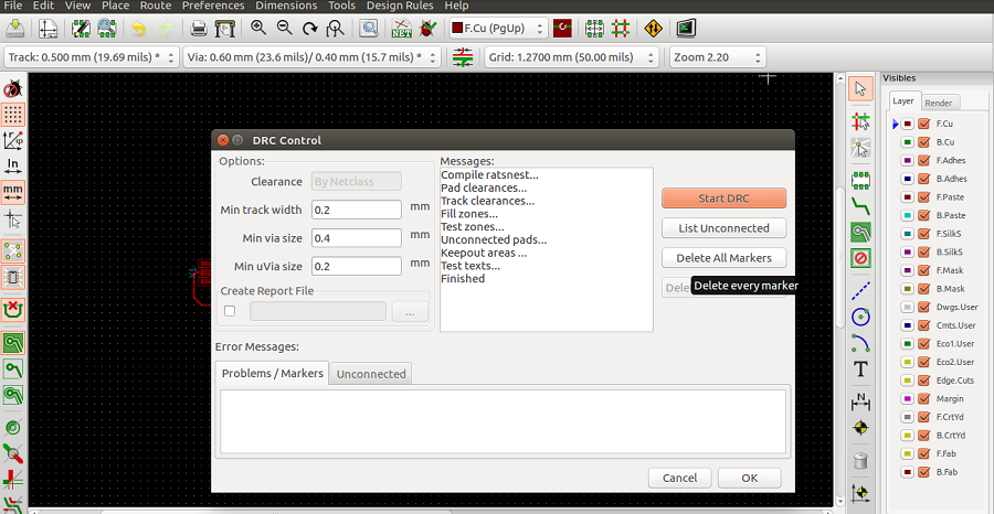
Arrange Components as you can . Click on the Add Traces and Draw the Tracks. After completing the process I just do DRC and Shows no errors.
Exporting the Design File
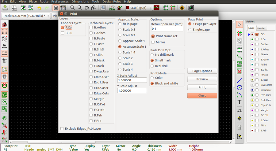
- Click file > print (select the required layer, click black and white) > then click print.
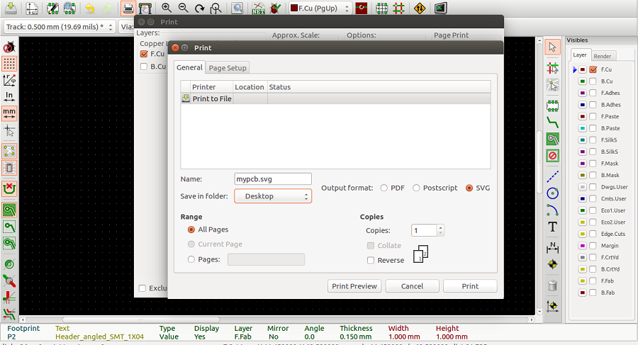
- Select the file to print, click SVG format and save.
- Open your svg format in inkscape and save as png.
Group Assignement
We need to Use the test equipment in your lab to observe the operation f a microcontroller circuit board,Equipements available in our lab are
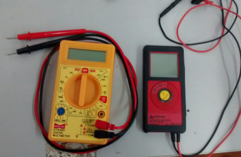
- Multimeter : A multimeter or a multitester, also known as a VOM (volt-ohm-milliammeter), is an electronic measuring instrument that combines several measurement functions in one unit.
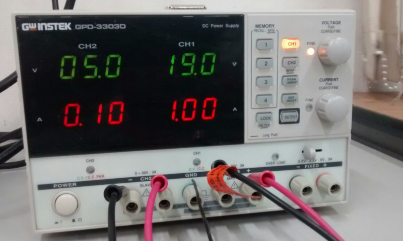
- Dual Channel power supply :
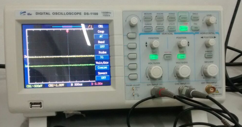
- Digital Oscilloscope: A digital oscilloscope is a complex electronic device composed of various software and electronic hardware modules that work together to capture, process, display and store data that represents the signals of interest of an operator.
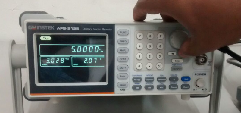
- Function Generator : An arbitrary function generator is a piece of electronic test equipment used to generate electrical waveforms