Week07 - Electronics Design
|
For this week's Assignment, i did this. 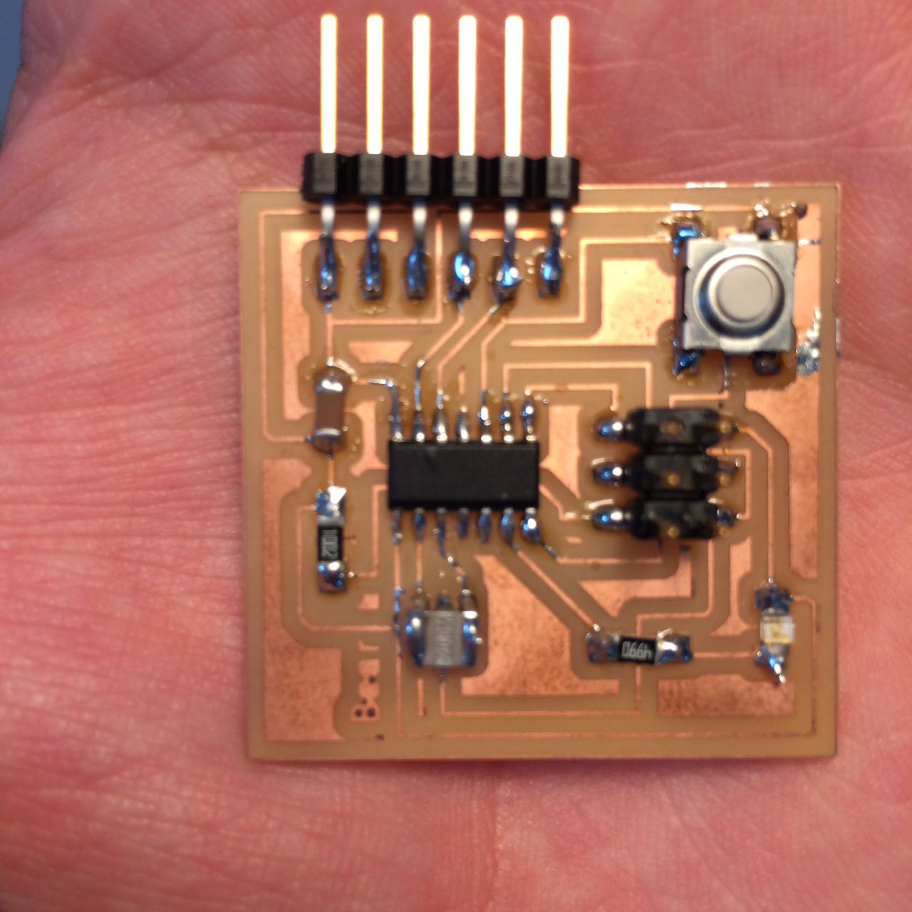
1-KiCadCNCing the traces is so much easier now that i already knew how, working on KiCad, the routing traces stage specifically, was like playing a puzzle game i know on the
ipad, its funny, i think playing that game actually helps with this xD KiCAD is basically an Electronic Design software. 
You have 2 Main stages to create a board like this board. Schematics and Board Design. SchematicsThe schematics page is where we put our components and link them logically together. it does not resemble how the board will look like, but it does have all of the board components. It is useful to have the schematics for an easy understanding of the boards, it is excellent for sharing with other people. Let me talk about few tools in the schematics stage. -Place Component: This tool is one of the most basic important tools here, it is used to add components to the schematics. 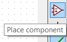
When you click on the icon, you will get the window below, where you are supposed to navigate and find your specific component to add in the schematics, for example the window is showing the AVRISP 6 pin header, if you want to add this component you click OK. There are lots of components already in the list like shown below if you notice the scroll bar. 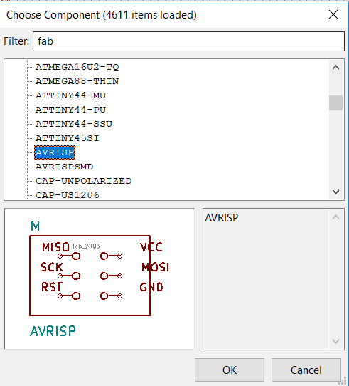
We however downloaded the fab library for components, if you notice above, the filter word is "fab". The fab library was provided for us in the Schedule section. I highlighted 2 libraries because i later switched to Eagle and it uses another Library format. 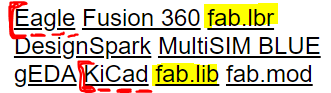
Download KiCAD fab.lib file here. To add fab.lib to KiCad you must go to preferences/Component library. Then just add the lib file. Note as you see below, the location of my lib is in Desktop, this is not best practice, as when you move it somewhere else, it loses the lib, so better move it to the common KiCAD lib folder. 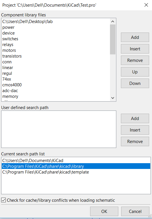
The individual assignment was very clear. redraw the board and add a at least 1 button and 1 LED, the LED will require a resistor to work. 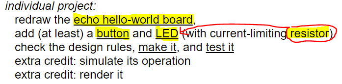
Here is the echo heloo-world board, i got it from here. 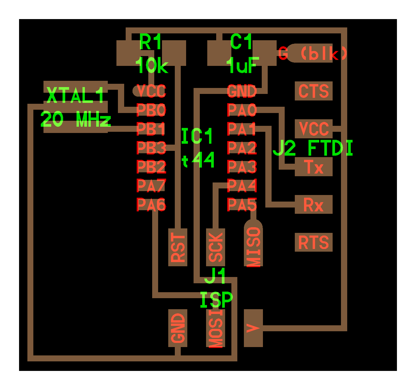
So i placed all the necessary components and the schematics looked like this! I will explain how i connected them below. 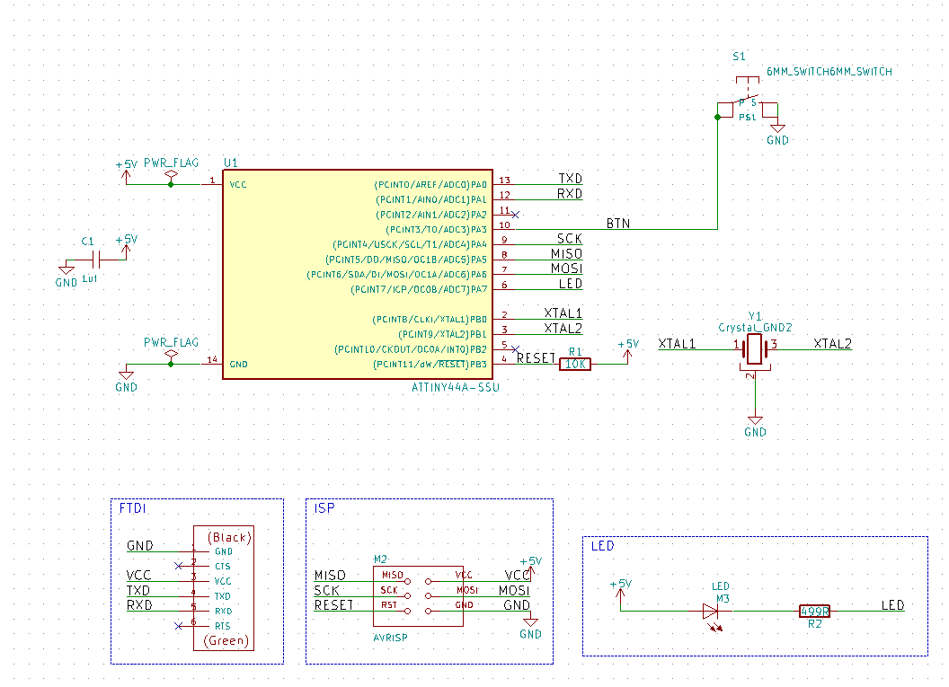
-Place Wire: This tool is used to connect pins together in the schematics. 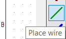
You do that by locating a circle at the end of the component pins, then you click inside and connect it to another component pin. 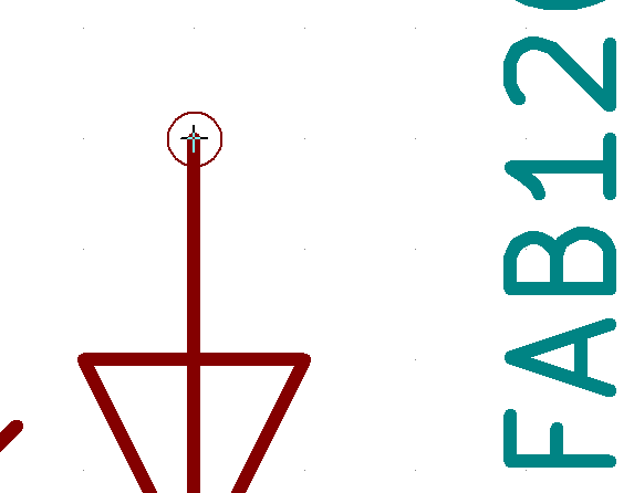
-Place Global Label: This tool offers another way of connecting pins together, you don't have to do a whole line to another pin, you can just give them both the same global label and let them free. 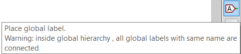
See how these pins are not connected to anything below, they are globally labeled, so they are connected with the pins on other components with the same global label. 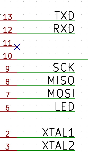
-Place Local Label: This is just like the global label, except it doesn't do anything buy to give the trace a label, it helps you when you want to understand what you are looking for faster. 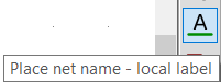
See it has the same process, you just click on it and write an informative tag, i wrote "something" below, and place it next to the wire. 
-Place Power Port: This tool lets you set a component, but its like special component that has invisible pins with names like GND. here is a link to a better explanation i found. 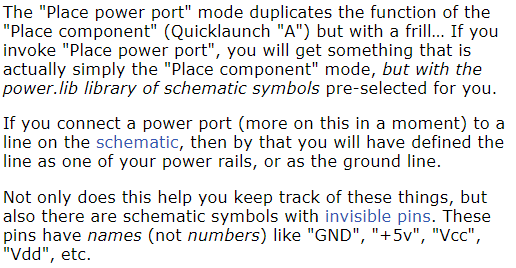
This is what the icon looks like below. 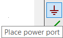
You get a window when you click on it, the window is just like adding a component window. 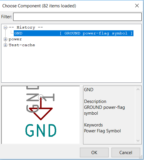
And then you just connect it simply at the end of a trace wire. Like this. 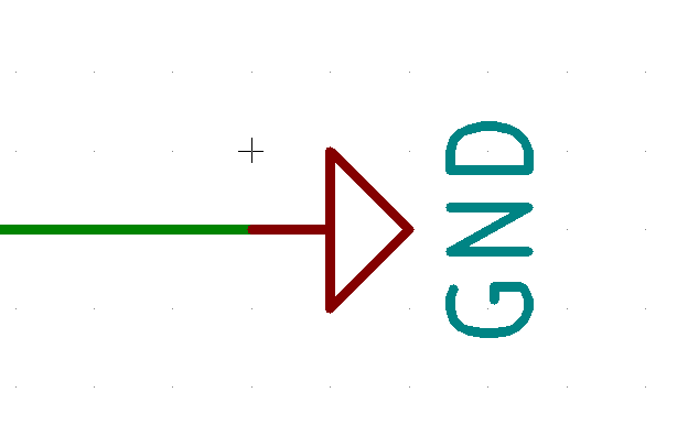
-Place Not-Connected Flag: This tool helps you clean your Electrical Rule Check(ERC) more about that below. 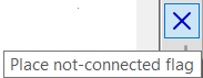
You simply place it on an unused pin like below. 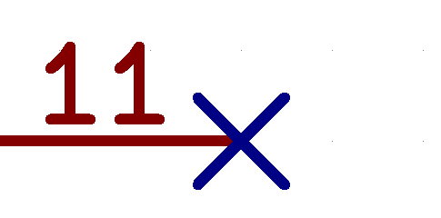 More about how it works below in the ERC. -Perform Electrical Rule Check: This button checks your electrical connections on the schematics, if something is either connected to nothing or connected to nothing, it shows here as a warning, it helps to remind you if you forgot something. 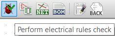
Using the above tool "Not-Connected", will help remove a problem such as shown below on the ERC window after you run the check. 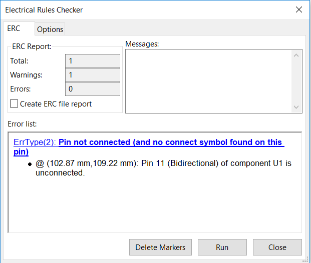
And it actually points at the schematics where you have an unconnected pin. 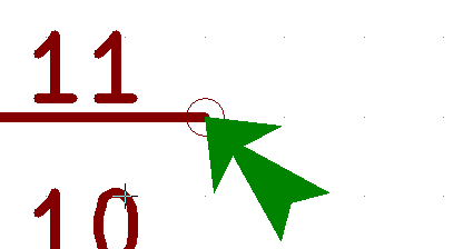
This is all about most tools i used in KiCad Schematics. Board DesignTo move from schematics to board design you click on this button. 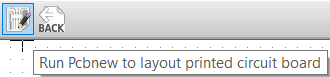
This will take you to the PCB view. 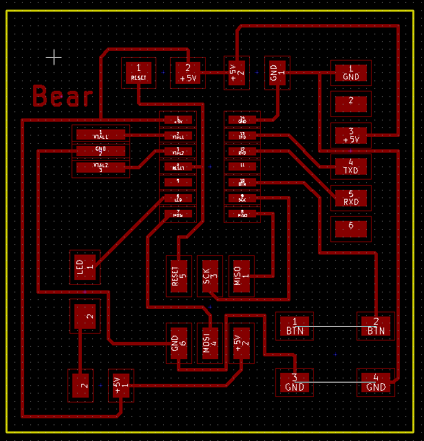
This is done with only 2 tools and few tricks. -Add Tracks: This is what we use to do the traces between components. 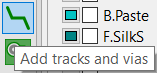
-Add Text: To make things more personal we also tested the text tool, i added my name on the board as you can see above. 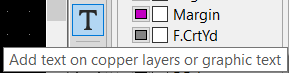
The text window is simple, you just type your text and confirm, then you pick where to place it. 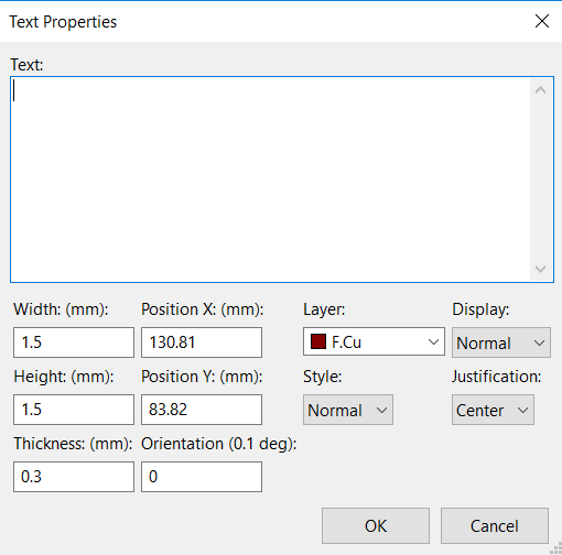
Perform Design Rules Check: This is just like the ERC but it is made for the Board Design view, it even has the same icon. 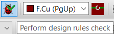
In the window, you just click Start DRC and check what problems you might get and try to fix them. 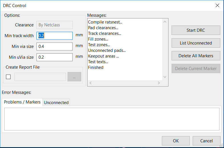
See i do have some unconnected pins, but that is irrelevant i don't need to connect them based on that component datasheet. 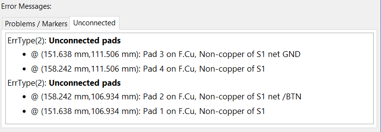
This is what you need to know to get started with tracing your boards. Next is to export it to a PNG, in KiCAD you can't do that, but you can however export it to an SVG, and that is what we did. 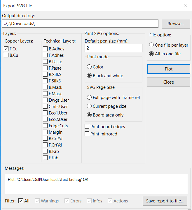
Make sure you check off the Technical Layers and Check the F.Cu because we are using only the front, we want it in black and white and then plot it. We opened the SVG file on Gimp software and made sure the dpi is set high 2000 is high. 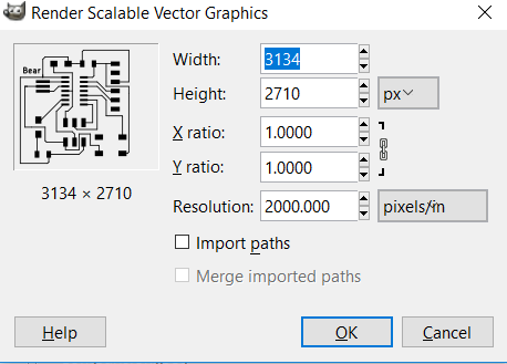
We used Gimp software here because it allows SVG to PNG Export and that is what we wanted, just make sure you put the compression to 0. 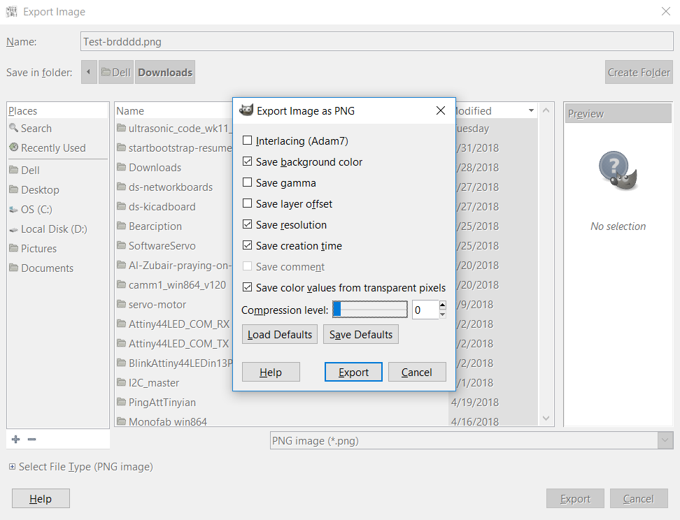
Next step is to go through fabmodules with the follwing PNGs, I did document the process in Week05 So refer to that. 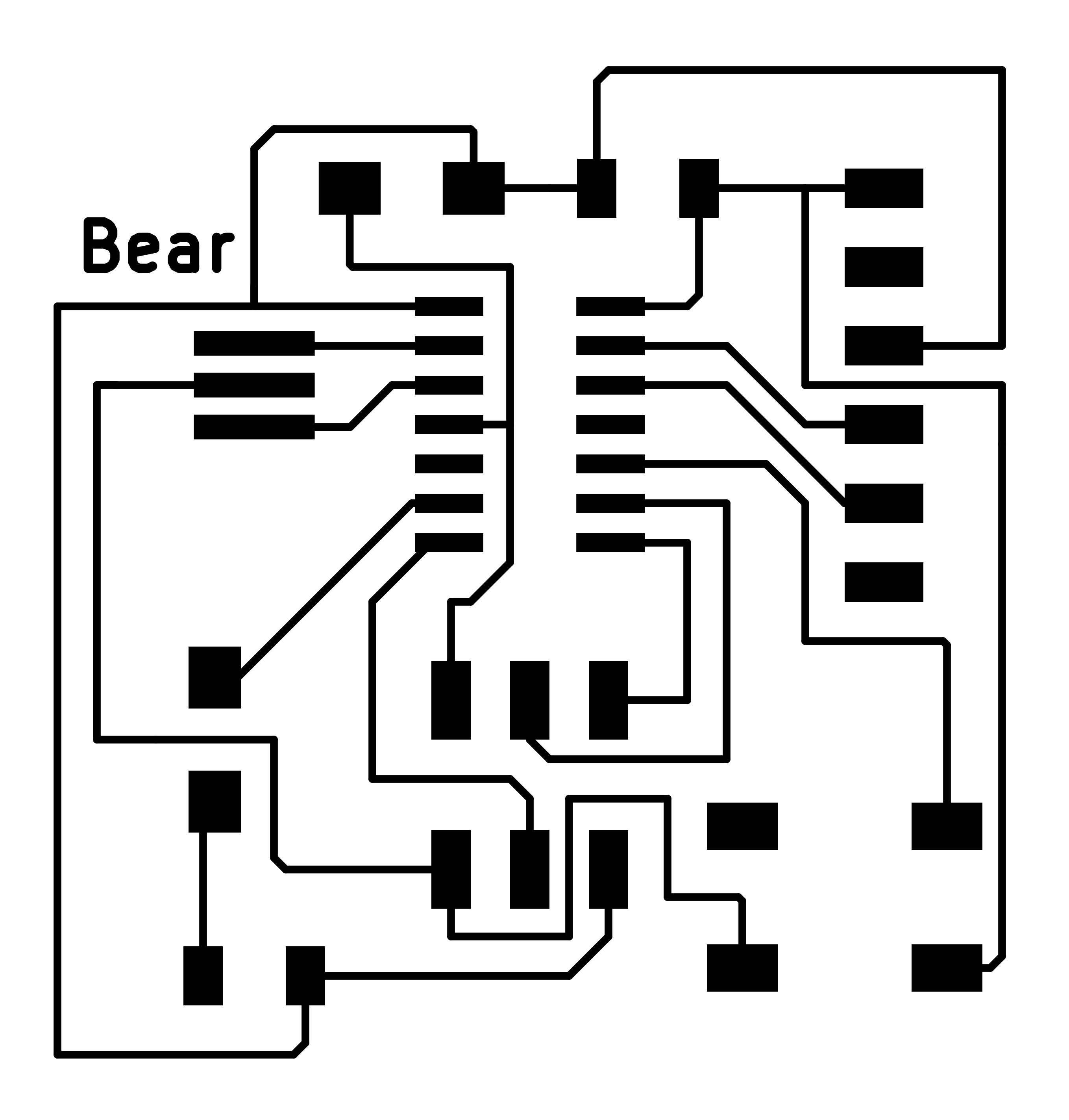

Then of course milled the board on the machine using the same 2 bits and process in Week05 and we got the board ready! Download KiCad file here. 2-SolderingEasy enough now that i am experienced. I do have a tip on soldering on Week05. 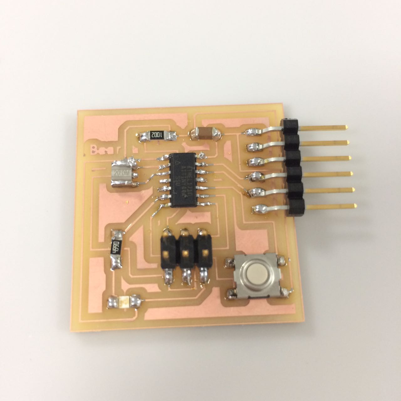
3-EagleWe had a session on Eagle with Hashim (2017 FabAcademyStudent) and i felt like it was much more comfortable to use than KiCad, it felt organized and neat which i liked. 
It was a lot similar and some things actually required more clicks, but KiCad had issues, like sometimes it doesn't show you everything on design because the software was either lagging or glitching, Eagle was just better. 3-Extra CreditI did program the board using the arduino example "Button" and this was the result. I wasn't clicking on the button i was just touching components. This was because i didnt use "INPUT_PULLUP" in the arduino code to activate the internal pullup resistor in the attiny on the button pin, a neat explination i found in this link here. It explains really well i can't compete! 
And now it works! 5-ProblemsHonestly doing the traces manually is a problem, at this point no one told us we could do the traces automatically, later i found out we could, but even then the software wasn't perfect. When the traces were impossible to calculate, the software didn't add jumper spaces on its own, but it did create holes to connect jumpers under the board, i guess that is something. Anyway what i ended up doing later on using Eagle, is using that auto route option and whenever i get 80% completed traces or something, i just add jumpers manually and continue the work on the left 20% of traces. Another problem i had was that my ISP Programmer suddenly wasn't recognized by my laptop, after a while of having multiple attempts on trying to fix it, resoldering it fixed it and i am proud! 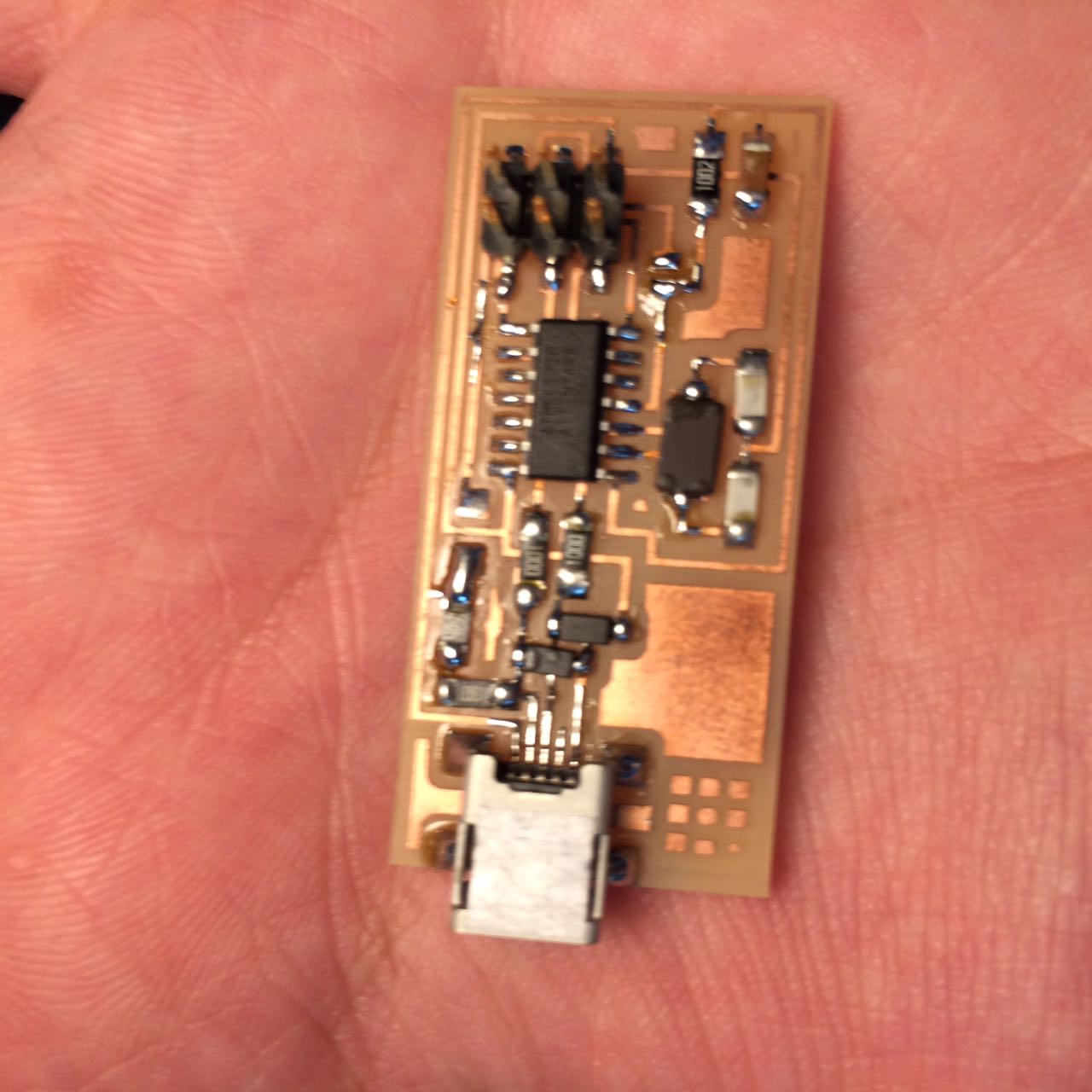
|