Networking & communications
april 25 - may 02
● The goal for this week's individual assignment:
design and build a wired &/or wireless network connecting at least two processors
group assignment:
send a message between two projects
● Planning to connect at least two of the boards with micro controllers on board with the help of serial bus by following the steps provided by Neil.
● I would also like to try the wireless communication between my input and output board using Bluetooth for my final project. Which might be really very challenging but I am looking forward to try soon.
getting started
I2c
● For this week I also decided to work on I2C protocol as the earlier job was not enough to show my understanding of communication, well, I didn't know much about this protocol as well but I know that using this protocol about 128 Microcontrollers can be connected together ..... each node is having its own address and the master of the netwrok can access any node using this address to have a better understanding of the I2C Protocol with ATTINY i followed this link.● Through this link a very good image of the protocol can be made and after going through this link I was able to understand how I2C works. But apart from understanding the protocol. Now it was the turn to realize this protocol. I was comfortable with Arduino IDE. So I was a bit confused how to realize this how to transmit standard data packets for the protocol etc etc . but after surfing through internet pages, the image of I2C using arduino became more clear and I got to know it was quiet easy to use with Arduino IDE Using Wire.h Library.every node can be identified by an address which we can designate and through this address master can communicate to any of the node
Overview Of I2C Protocol
● The Inter-integrated Circuit (I2C) Protocol is a protocol intended to allow multiple “slave” digital integrated circuits (“chips”) to communicate with one or more “master” chips. Like the Serial Peripheral Interface (SPI), it is only intended for short distance communications within a single device. Like Asynchronous Serial Interfaces (such as RS-232 or UARTs), it only requires two signal wires to exchange information.Why Use I2C? What’s Wrong with Serial Ports?
● Because serial ports are asynchronous (no clock data is transmitted), devices using them must agree ahead of time on a data rate. The two devices must also have clocks that are close to the same rate, and will remain so–excessive differences between clock rates on either end will cause garbled data.
● Asynchronous serial ports require hardware overhead–the UART at either end is relatively complex and difficult to accurately implement in software if necessary. At least one start and stop bit is a part of each frame of data, meaning that 10 bits of transmission time are required for each 8 bits of data sent, which eats into the data rate.
● Another core fault in asynchronous serial ports is that they are inherently suited to communications between two, and only two, devices. While it is possible to connect multiple devices to a single serial port, bus contention (where two devices attempt to drive the same line at the same time) is always an issue and must be dealt with carefully to prevent damage to the devices in question, usually through external hardware.
● Finally, data rate is an issue. While there is no theoretical limit to asynchronous serial communications, most UART devices only support a certain set of fixed baud rates, and the highest of these is usually around 230400 bits per second.
Why Use I2C? What’s Wrong with Serial Ports?
● The most obvious drawback of SPI is the number of pins required. Connecting a single master to a single slave with an SPI bus requires four lines; each additional slave requires one additional chip select I/O pin on the master. The rapid proliferation of pin connections makes it undesirable in situations where lots of devices must be slaved to one master. Also, the large number of connections for each device can make routing signals more difficult in tight PCB layout situations. SPI only allows one master on the bus, but it does support an arbitrary number of slaves (subject only to the drive capability of the devices connected to the bus and the number of chip select pins available).
● SPI is good for high data rate full-duplex (simultaneous sending and receiving of data) connections, supporting clock rates upwards of 10MHz (and thus, 10 million bits per second) for some devices, and the speed scales nicely. The hardware at either end is usually a very simple shift register, allowing easy implementation in software.
Enter I2C - The Best of Both Worlds!
● I2C requires a mere two wires, like asynchronous serial, but those two wires can support up to 1008 slave devices. Also, unlike SPI, I2C can support a multi-master system, allowing more than one master to communicate with all devices on the bus (although the master devices can’t talk to each other over the bus and must take turns using the bus lines).
● Data rates fall between asynchronous serial and SPI; most I2C devices can communicate at 100kHz or 400kHz. There is some overhead with I2C; for every 8 bits of data to be sent, one extra bit of meta data (the “ACK/NACK” bit, which we’ll discuss later) must be transmitted.
● The hardware required to implement I2C is more complex than SPI, but less than asynchronous serial. It can be fairly trivially implemented in software.
Protocol
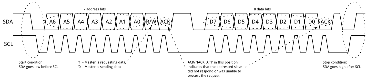
● Messages are broken up into two types of frame: an address frame, where the master indicates the slave to which the message is being sent, and one or more data frames, which are 8-bit data messages passed from master to slave or vice versa. Data is placed on the SDA line after SCL goes low, and is sampled after the SCL line goes high. The time between clock edge and data read/write is defined by the devices on the bus and will vary from chip to chip.
Start Condition
● To initiate the address frame, the master device leaves SCL high and pulls SDA low. This puts all slave devices on notice that a transmission is about to start. If two master devices wish to take ownership of the bus at one time, whichever device pulls SDA low first wins the race and gains control of the bus. It is possible to issue repeated starts, initiating a new communication sequence without relinquishing control of the bus to other masters; we’ll talk about that later.Address Frame
● The address frame is always first in any new communication sequence. For a 7-bit address, the address is clocked out most significant bit (MSB) first, followed by a R/W bit indicating whether this is a read (1) or write (0) operation.● The 9th bit of the frame is the NACK/ACK bit. This is the case for all frames (data or address). Once the first 8 bits of the frame are sent, the receiving device is given control over SDA. If the receiving device does not pull the SDA line low before the 9th clock pulse, it can be inferred that the receiving device either did not receive the data or did not know how to parse the message. In that case, the exchange halts, and it’s up to the master of the system to decide how to proceed.
Data Frames
● After the address frame has been sent, data can begin being transmitted. The master will simply continue generating clock pulses at a regular interval, and the data will be placed on SDA by either the master or the slave, depending on whether the R/W bit indicated a read or write operation. The number of data frames is arbitrary, and most slave devices will auto-increment the internal register, meaning that subsequent reads or writes will come from the next register in line.Stop condition
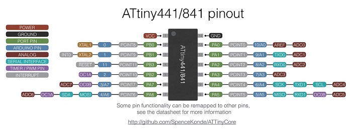
● Once all the data frames have been sent, the master will generate a stop condition. Stop conditions are defined by a 0->1 (low to high) transition on SDA after a 0->1 transition on SCL, with SCL remaining high. During normal data writing operation, the value on SDA should not change when SCL is high, to avoid false stop conditions.~Source: Sparkfun ● Now that we understand about I2C we need to go through the pin Diagram of the ATTINY 44 to identify SDA and SCL pins, These pins would be used for I2C Communication.
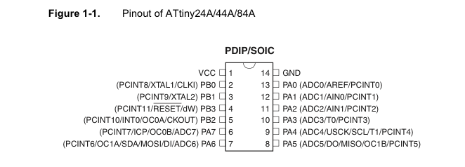
● From the diagram it may be noticed that PA6 and PA4 are the SDA (Serial Data) and SCL (Serial Clock), these pins would be furthur considered while designing the PCB.
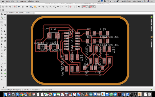
● Now that the I was able to understand I2C protocol and confident to code the controllers. I started with making the board files for the master and slave . I went through Labs inventory first to check the availability of the components and then moved furthur to make PCB on Eagle.
Download the Eagle Board Files
HERE
● The below one is for the master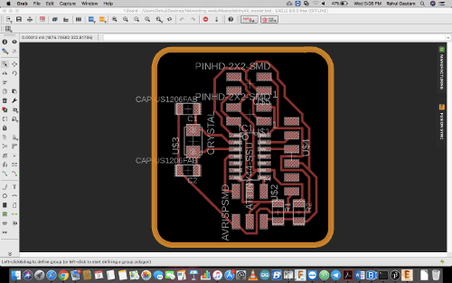
● This one is for the slave
● Milling and Soldering Now since my design was ready , The designs were ready to mill and after milling
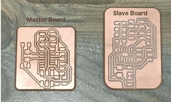
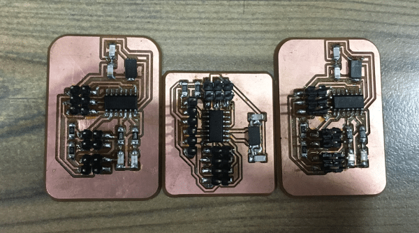
● Now after milling the boards I soldered all the components on the board ....... and here is the Hero Shot of the same .....
I made 2 slave boards and 1 Master Board
Connections ● Now for making a network we need to connect all the boards together...... for connections this is a schematic, how to connect the slave boards to master.
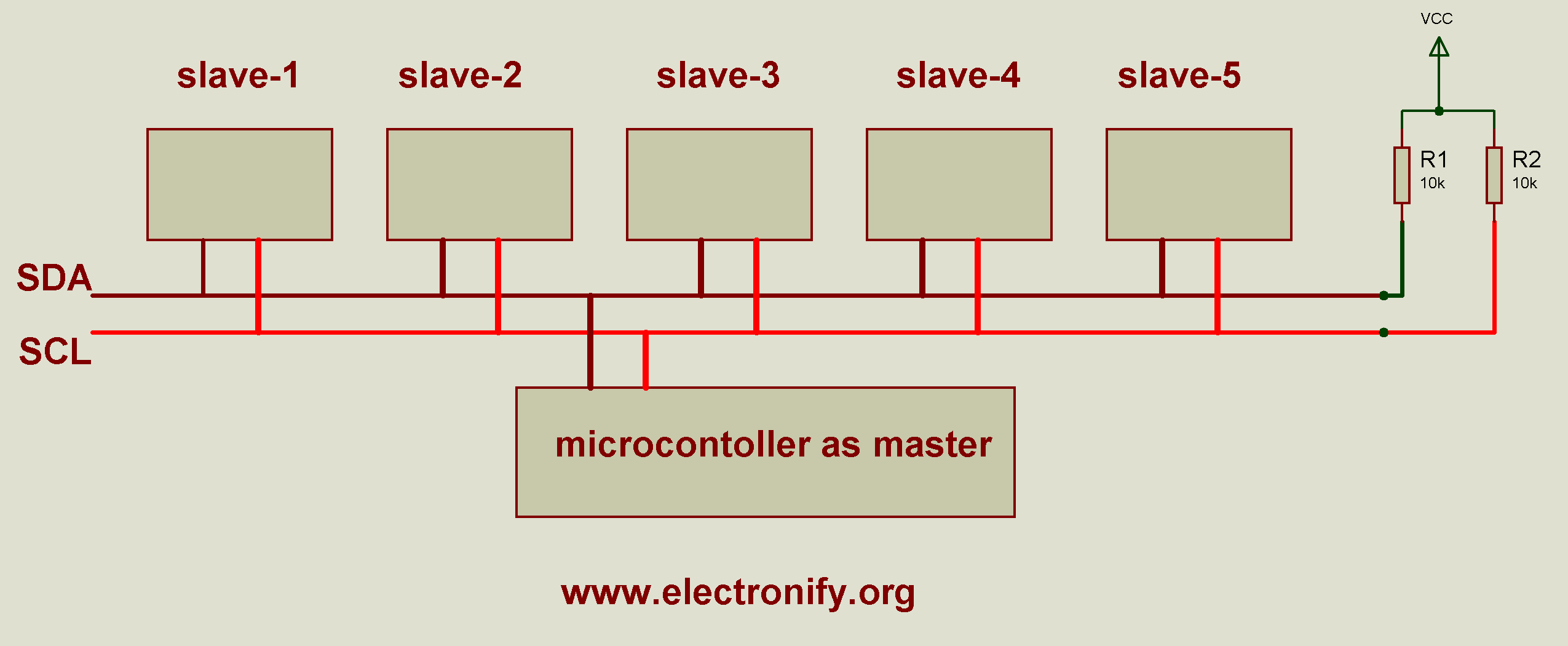
Pic Courtesy : www.electronify.com
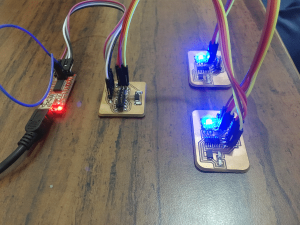
● Actual Connections
Download the Programming codes
HERE
Master Code
#include "Wire.h" // This is I2C library
#include "SoftwareSerial.h" // This is used for making rx tx pins using software
#define Rx 0
#define Tx 1
SoftwareSerial myserial(Rx, Tx); // declared Rx and Tx Pins

void setup() {
  Wire.begin(); // I2C communication Started
  myserial.begin(9600); // Serial communiation Started
  myserial.println("Communication Started");
}

void loop() {
  char d; // Character type declaration to store a character.
  if (myserial.available() > 0)
  {
    d = myserial.read(); // Read serial and store its value in variable d.
    if (d == '1') {   // Now transmit data over the I2C lines according to the cases.
      Wire.beginTransmission(1); // Communication started with first node
      Wire.write(1); // Value sent over the channel
      Wire.endTransmission(); // Communication Ended
      myserial.println("send :- ");
      myserial.print(d); // Print on Serial Monitor

    }
    if (d == '2') {             // Same of others.
      Wire.beginTransmission(1);
      Wire.write(2);
      Wire.endTransmission();
      myserial.println("send :- ");
      myserial.print(d);

    }
    if (d == '3') {
      Wire.beginTransmission(2);
      Wire.write(3);
      Wire.endTransmission();
      myserial.println("send :- ");
      myserial.print(d);

    }
    if (d == '4') {
      Wire.beginTransmission(2);
      Wire.write(4);
      Wire.endTransmission();
      myserial.println("send :- ");
      myserial.print(d);

    }

  }
  delay(10); // Delay to make sure whole CPU is not consumed.
}
Note: To understand the code read comments
Slave Code 1
Slave Code 2
Note: To understand the code read comments
Bonus Info on I2C Protocol
● The I2C bus is a standard bidirectional interface that uses a controller, known as the master, to communicate with slave devices. A slave may not transmit data unless it has been addressed by the master. Each device on the I2C bus has a specific device address to differentiate between other devices that are on the same I2C bus. Many slave devices will require configuration upon startup to set the behavior of the device. This is typically done when the master accesses the slave's internal register maps, which have unique register addresses. A device can have one or multiple registers where data is stored, written, or read.● The physical I2C interface consists of the serial clock (SCL) and serial data (SDA) lines. Both SDA and SCL lines must be connected to VCC through a pull-up resistor. The size of the pull-up resistor is determined by the amount of capacitance on the I2C lines
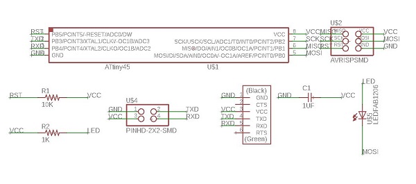
BELOW IS THE EARLIER ASSIGNMENT. ● To start with, based on Neil's board for Bridge and Node, I redrew the bridge and Node board to carry out the communication process.
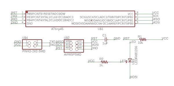
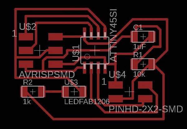
● The bridge board contains basic components such as ATtiny45, FTDI, AVRISP header, one more 2x2 header, Two Resistors (1k & 10k), One Capacitor (1uF) and an LED.
● I started designing on Eagle because by now, I am quite used to Eagle, so as per the components I created the schematic as shown below. I labeled and named the components and placed the wires for connection as well in the schematic.
● Then the next step was the design the actual traces for the board and make sure that no trace crosses the path of the other trace.
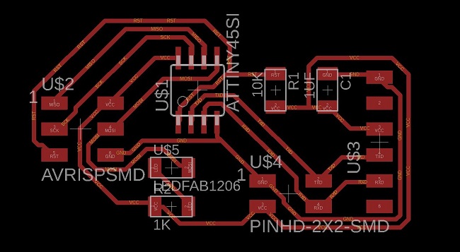
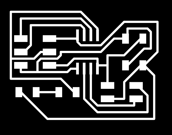
● The image shows the (.png) file Bridge Board designed on Eagle.
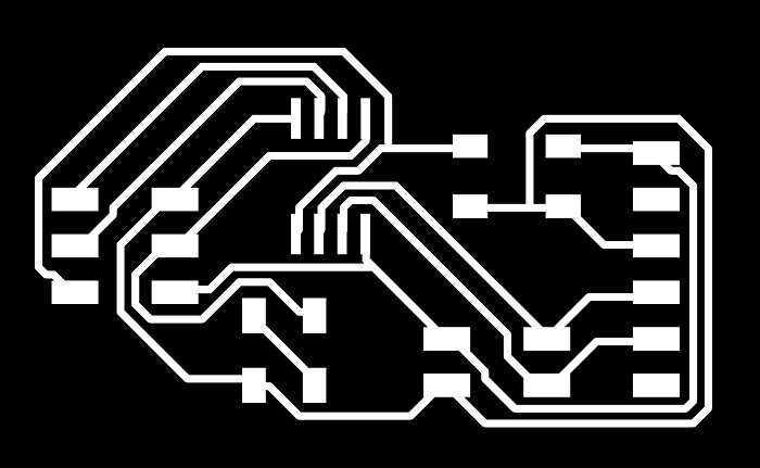
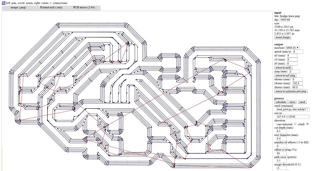
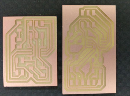
● Then I used fab modules to create the (.rml) file to cut the board on Roland Machine
● I followed the same steps to design the node board and used all the same components except the FTDI, because the node board did not the FTDI to connect it to the machine.
● The following image shows the board and the PNG file for the Node board.
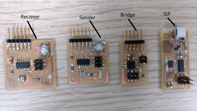
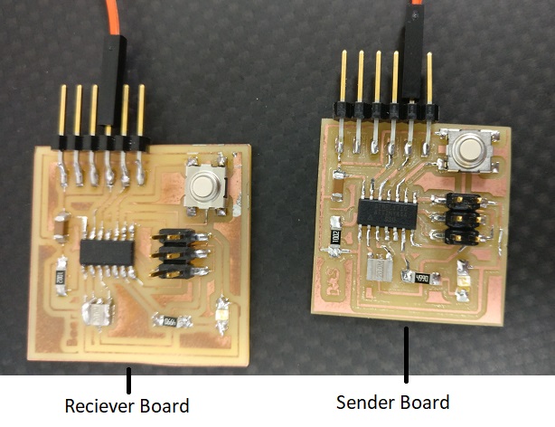
● I must admit, the above board designs and production done on Eagle was a much needed practice session for me, I feel more confident using Eagle now, selecting the components based on Neil's board, creating the traces and using the Roland machine. Having said all of the above, I won't be using the node board for this week's assignment. Rather than investing more time, as I was lagging a little behind on schedule it was better for me to just use the bridge board and to use the boards which were designed and produced by me during design week and tested during Embedded Programming weekfor sender and receiver, to carry on with this particular serial bus communication.
● For two reason, to save time, which was essential and also because I knew for sure that the board that I made earlier in the course were working perfectly fine, so I decided to work with the Board that I had designed during the Electronics Design week and to use it a the sender board.
● Next step in order to complete this week's assignment was to program the Boards using the FABISP that I created in the Electronics Production week.
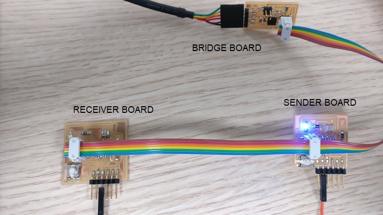
● The below image shows all the boards used by me to complete this assignment.
● It was of utmost importance to make sure of the connections and also the code and then progressively programme them to communicate.
● I used the FABISP to program my sender and receiver boards, and also used the Bridge board in the final process of Serial Bus operation, so basically the bridge board powers the sender and receiver boards with a daisy cable, through its connection to the laptop via the FTDI cable. The sender code has been programmed in such a way that once the push button is pressed, it transmits a specific number(2, in this case) through the Tx pin on the FTDI which is then received by the receiver board through the receiver pin on the FTDI, to showcase the pattern of loop function and turn the LED ON and OFF as per the code uploaded.
● Eidha and Zubair also helped me in order to understand how the code works. Because even they faced similar challenges, that we were successful to programme the boards but they would not communicate with each other.
● I tried programming the sender and receiver board a lot of times and found success using the codes below.
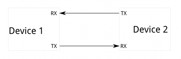
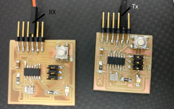
● It was important to make sure of the way the sender and receiver were connected through RX, TX which stands for receiver and transmitter, which are used to perform respective functions to transfer data. The code enabled me to understand the RX and TX have to be connected in the following manner for the sender and receiver board to communicate.
● The original code has been sourced from my dear friend and fellow student at the Fabl Lab UAE, Eidha Al Rashdi, special thanks to him for making me understand the code in a nice way that I could learn and then work on it further. I did modify the code in terms of the serial character used by me for serial communication, to define the pins for the LED and the button, also modified the loop routine according to my idea for serial communication.
● Download the modified Arduino sender code for serial bus HERE
SENDER CODE
● Download the modified Arduino sender code for serial bus HERE
RECEIVER CODE
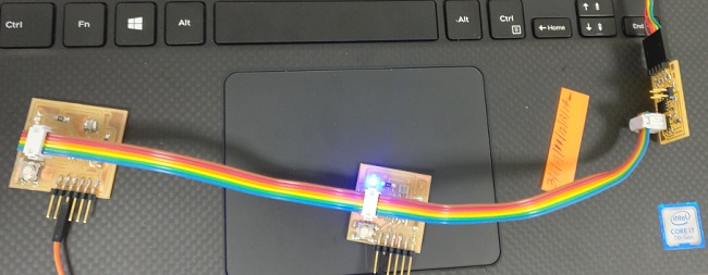
● And finally, after a determined effort from myself and Alzubair, who was also working with me for his this week's assignment as well, made the serial communication possible shown in the video below.
serial peripheral interface
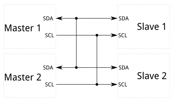
● Wendy suggested me to go through this really informative tutorial LINK for the serial periphery interface (SPI) in order to understand the significance of creating a serial interface with the help of the information it provided.● In the assignment completed by me, I used the serial ports to make a communication between two microcontrollers using the RX and TX ports on the FTDI header. After going through the SPI tutorial I learned that this kind of communication is regarded as asynchronous because there is no control over when data is sent or any guarantee that both sides are running at precisely the same rate. Even though it's possible to communicate, but it is not the recommended process to follow for this kind of serial bus.
● Reading more in detail about the synchronous solution, I found out that, it works in a different manner, which means it uses seperate lines for data and a 'clock' that keeps both sides in perfect sync. One more reason that SPI is so popular is that the receiving hardware can be a simple shift register. This is a much simpler and inexpensive piece of hardware that the full-up UART (Universal Asynchronous receiver/transmitor) that asynchronous serial requires.
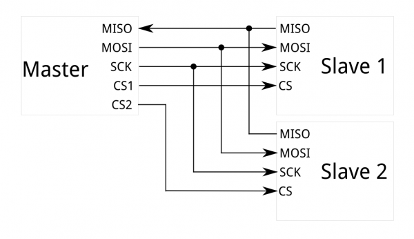
● Below image explains multiple ways to connect the network, taking guidance for the ATtiny pinout in order to make sure of the correct pins, their connections and the functions of the same.
- each slave will need a separate SS line. To talk to a particular slave, you’ll make that slave’s SS line low and keep the rest of them high (you don’t want two slaves activated at the same time, or they may both try to talk on the same MISO line resulting in garbled data)
On the other hand, some parts prefer to be daisy-chained together, with the MISO (output) of one going to the MOSI (input) of the next. In this case, a single SS line goes to all the slaves. Once all the data is sent, the SS line is raised, which causes all the chips to be activated simultaneously
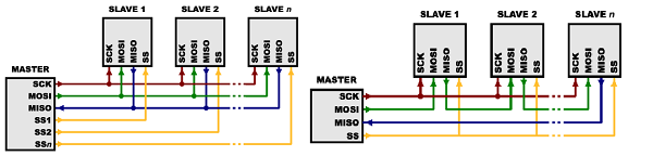
● I learned that I can create a system of communication by implementing the above SPI and connect multiple slaves for SPI bus using the ISP header while choosing the MOSI,MISO,SCK,Select Slave pin in order to initiate the communication.
● It wouldn't say I understood each and every thing but I definitely made an effort to try to grasp as many essential aspects about the SPI that I could and also learned more through the ATtiny44 pinout in order to understand the connections to be done with regards to create a network of communications involving multiple which can also be increased to make a whole system. I wish to carry out the same sometime soon making use of the pins available on ISP header to set up a serial bus for multiple slave and single master.
● I also tested the code on three boards for developing a serial bus though the ISP header pins by assigning the MISO as TX and the SCK as RX pins respectively. From the above tutorial I learned that I can set up a network of multiple slaves and with one master, without using the FTDI cable for communication, instead using the ISP header is much easier and effecient way to do the same. I can have a two way communication in the similar pattern, with a host and multiple slaves with an accurate form of addressing where once the slaves receive a particular alphabet or any character as per the code from the master host and by reading that the slave boards light up through the LED or perform the task as per the code which hsa been programmed. In the same way the host could also receive data from the slave.
● The video attached below works on the same aspect of networking and communication working on three boards. I am away from the lab for the time being, as I have to sort my visa proceedings and other important commitments, so I could not use the above example extensively and I shall implement communication that use some form of addressing as explained above, a master and two slaves, which is very essential, having said that I am at a very good position where I understand the process of networking and communication and I shall implement the same extensively in near future, If i get an opportunity to do the needful at the FAB14 conference, I shall definitely do it. I acknowledge Zubair, for helping me out with his video.
● Downlaod the Receiver code
● Download the Transmittor code
learning outcomes
● Download the KICAD Sender & Receiver Board File HERE● Download the (.png) file for the Sender and Receiver Boards HERE
● Download the Eagle Bridge and Node Board file HERE
● Download the (.png) file for Bridge Board HERE
● Download the (.png) file for Node Board HERE
● A fun and exciting week leads to more valuable lessons and challenges, learned quite a lot about how to create a communication between two PCBs and this will help me a great deal in the final project.
● Very interesting week to get a chance to experience and learn networking and communication. I am looking forward to actually apply this week's work to my final project for wireless communication.