Electronics Production
What is the assignment?
In this week we have two assignment the first one is group assignment we must characterize the specifications of your PCB production process. The second assignment is individual, so I must mill the PCB to make an in-circuit programmer. In this week we will only mill the PCB we will not drill it nor design it.
The Goals
My goal is to learn more about CNC that we will use and practice soldering till I get comfortable.
In this Page you will find:-
Building the PCB
The individual assignment is to mill the PCB. I wasn’t here when Wendy explains the assignment I was working on a Hypred car to participate in the competition that will be in March this year. So thanks to my friend Carl he explained to me this week task. So we must build FabISP(In System Programmer) which allow is to put codes from the labtop into it to upload it to another microcontroller.
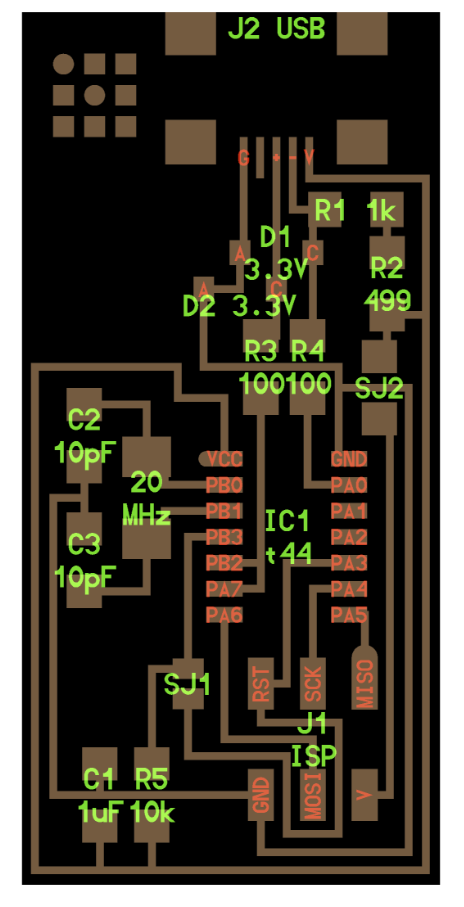
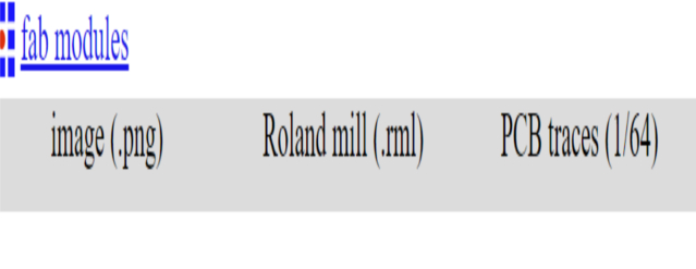
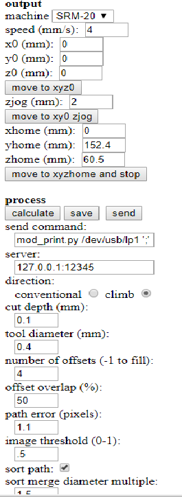
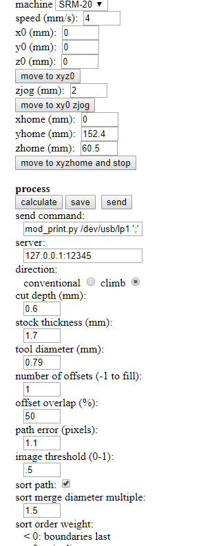
The first thing is to download the traces and interior and then I opened Fabmodule which allow me to decide the reference point also to calculate the tool paths. When I opened the Fabmodule I chose from the input image(.png) then I chose the image then Output format I chose (.rml) because we use SRM-20, in the process we chose PCB traces (1/64) to mill the PCB.
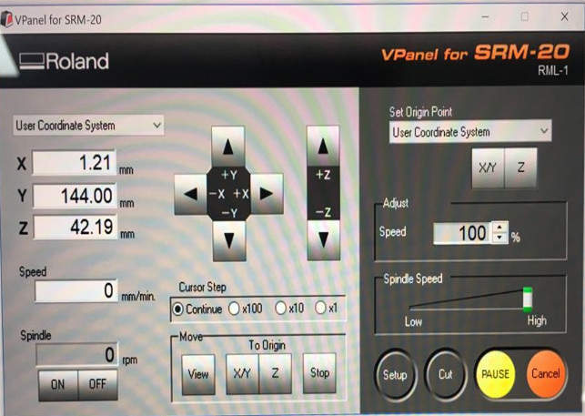
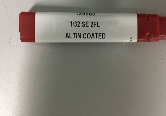
Then in machine, I chose SRM-20 and I put the X, Y, and Z to zero(the reference points) and then I clicked calculate to see the tool path and then save but since Wendy set it up there is no need to click save because its ready but I now that when I will click save (.rml) file will download to take it to the CNC software which will be for milling the traces. You can see in the images below the sitting in the fabmodules such as depth of cut which is 0.1 for the traces and 0.6 for the outline. also the diameter of the 1/64 bit which is 0.4mm and 0.79 mm for 1/32
After that, I opened the Vpanel which is for this type of CNC.
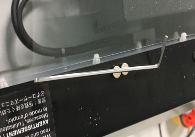
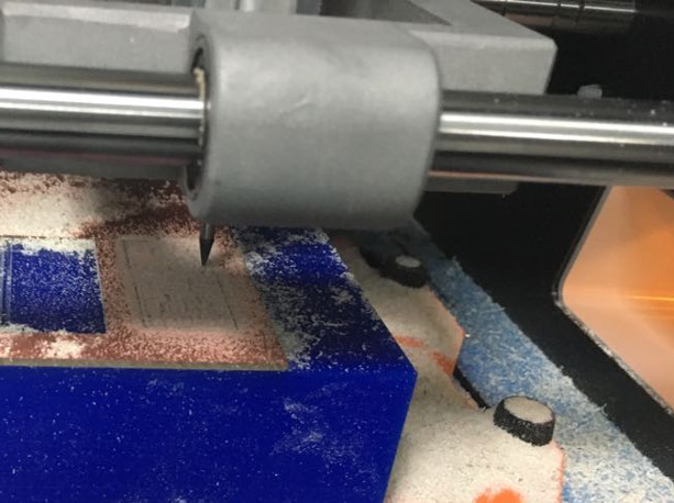
I looked inside the CNC to make sure there is a board on top of the sacrificial layer.
The sacrificial layer is made of wax and we stick the copper on top of it to not move. We put sacrificial layer because when we want to cut through the PCB we need to make the depth of the cut more than the thickness of the copper plate. we use always this sacrificial layer on all CNC machines.
Then in the Vpanel I set Y and X by moving the table using the arrows, I can adjust the distance it moves when I press the arrow by changing the speed from the bar below the arrows there is four choices continue, x100, x10, and x1 for example if I choose x100 every time I click the arrow the drill will move 1mm and so on. So then I checked the bit it was 1/32, so I change it by using the Key to unlock the bit.
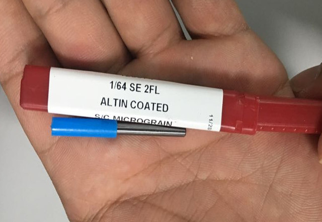
I changed bit 1/32 to bit 1/64 which is for milling. 1/32 and 1/64 mean the diameter of the bit.
When assembling the bit I put more inside because when I want to set the Z coordinate I just move down the drill until it becomes 1 cm from the board then I unscrew the bit and drag it until it touches the board then I lock the bit, by doing this I set the z-axis to zero. Also after I set the Z-axis I must left the bit up of the copper plate to not by mistacke press the arow down and hit the plate then dameg the bit. After I set the coordinate I went to the Vpanel and click on Cut to add the file, I cant click cut or move to origin until the door is closed. After I added the (.rml)file from the flash I clicked on output and then immediately I put the mouse on pause in case something wrong happened. The CNC start milling it take 3-4 minute.
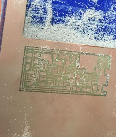
When I finished I took a wet tissue I don't want to blow because it will come on my I so the best way is to clean the PCB with a wet tissue to see if traces correct.
Then I changed the bit and put 1/32 to cut the borders so I can take them. I did the same process and then I set the Z only because when changing the bit the reference point will change. Then I chose the border file then I clicked output and I put the mouse in the pause in case something happens.
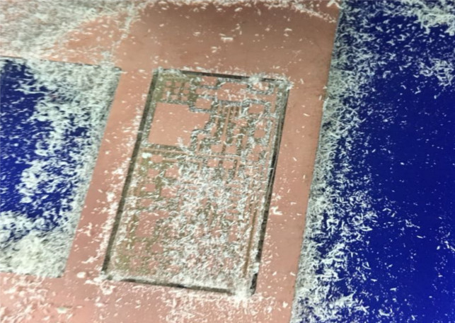
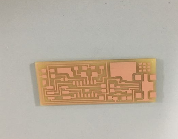
After that, I took off the PCB and I bring a roller to move it above the PCB to remove swarf. Now I the PCB is ready for the component.
Soldring and Testing
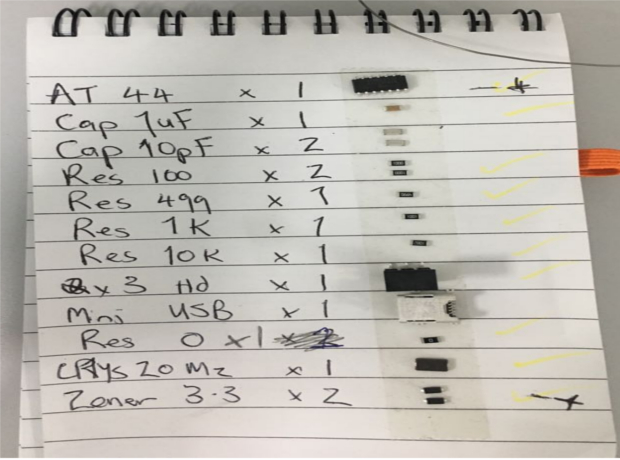
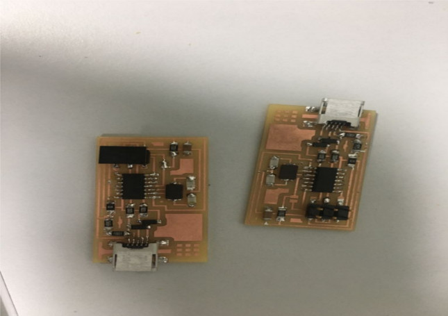
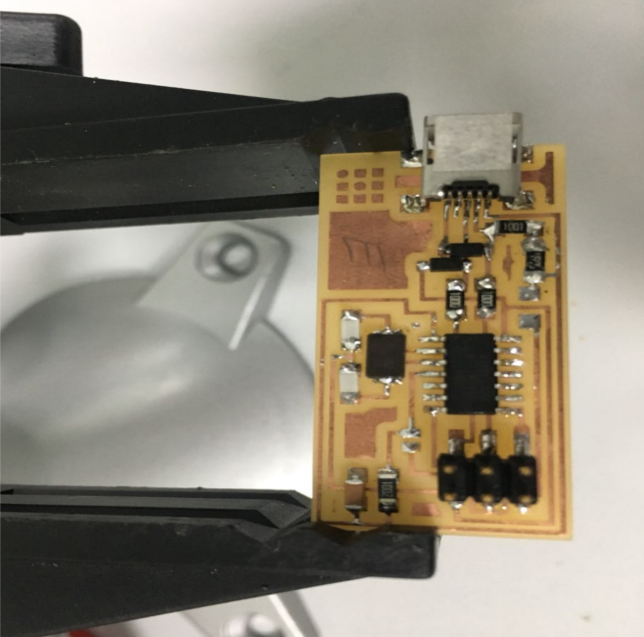
Now I must solder the component the (image is missing the zero-Ohm resistor). So I collect the component which is this.
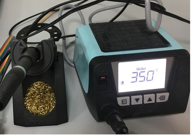
I start soldering the component it wasn’t easy. I make it 350C because in college we used to make it like this, but then Carl told me to make it 320C to not damage this small component)It requires patience and focusing skills, and you must be careful where to solder to avoid connecting two lines. The soldering took time from me it was annoying like I cant fix the component. The difficult thing is to solder the first leg. I accidentally few times connect two lines by soldering material but I succeed in removing them.
So finally I finish soldering I learn a way that makes me finish the last 5 component quickly which is soldering the place of the component in the PCB then grab the component and attached to that place and then all that you have to do is just to melt the solder then it will be stuck to the component and then you can easily solder the other leg. So after I finish soldering the PCB I still have to check the PCB. So I visually see if there is a short circuit or if the solder joint is not shiny because this will affect the connection.
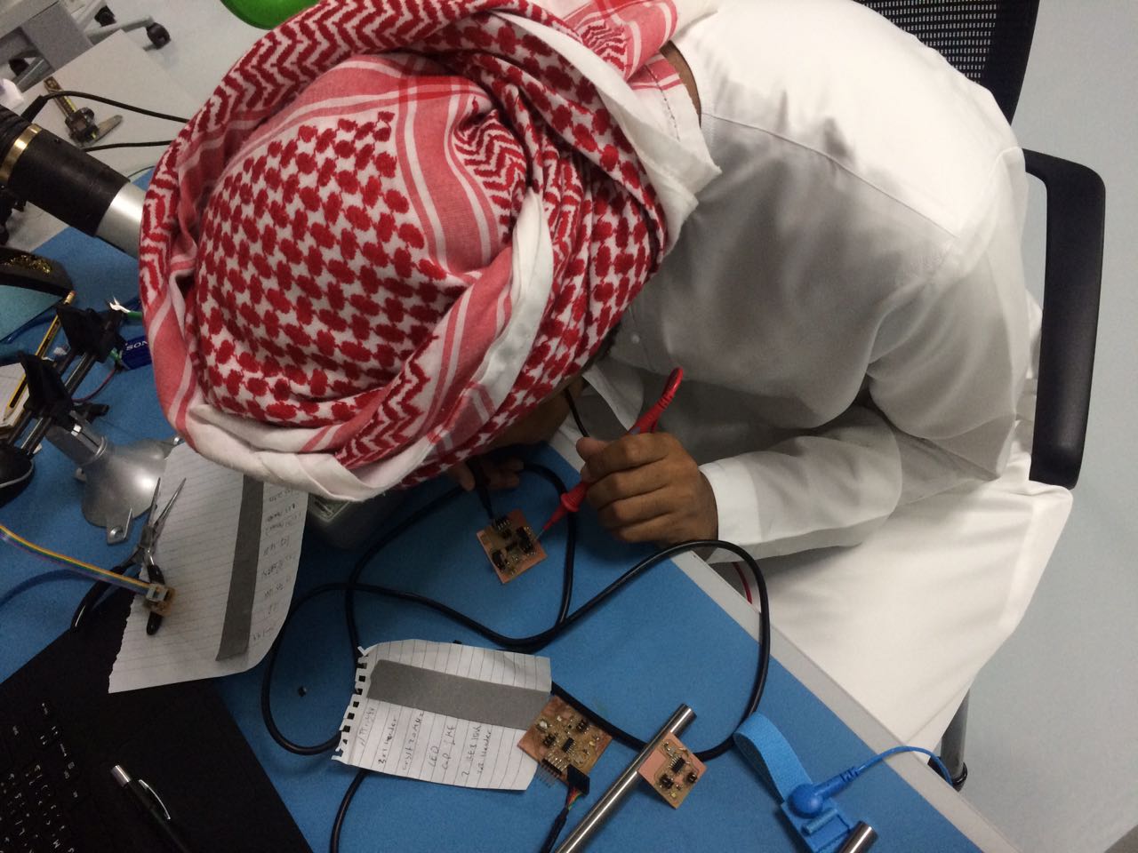
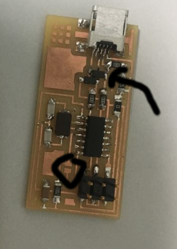
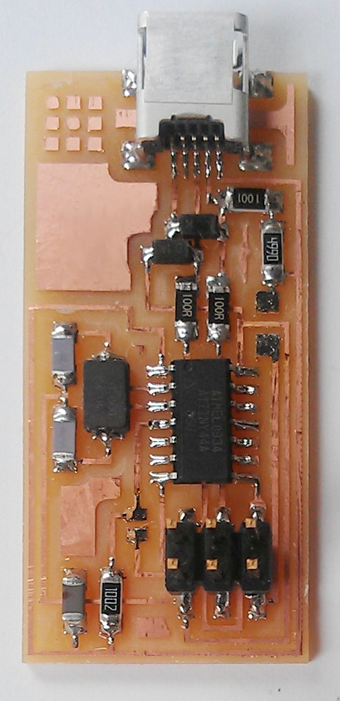
Then I checked the connection by using the multimeter. In order to check, put the first connector for example in the GND of the attiny44 and second connector in the GND of the header if you heard a buzz that means there are connected to each other and there is a connection if not you better check your circuit or the way you soldered. I found one problem in connection which is this I accidentally cut this line (image below) when I put a connector in the second leg of the mini USB and the other in the 100-ohm resistor there was no sound so I made a soldering to connect the two line. Also, another testing was the smoke test which is plugging the PCB to the laptop, if there were smoke that means your PCB is not good thanks, god mine was OK.
Programing
I used two tutorials: this to download the software and this to see the steps of programming. Because I wasnt here on Sunday, Windy expline to others how to program. When I came in Monday I saw Wendy working to prepare for Dubai MINI marker fair. She told me to see the tutorials and download the software. I went to download I found some of them are broken so you can find them all here which are for Windows users( not to mention that you must download git bash):
The drivers for your version of Windows
The FabISP Firmware
WinAVR
Zadig
Atmel AVR Toolchain for Windows
Gnu Make
avrdude
Then Zahrah came and Wendy asked her to help me so I saw what is the next step it told me to set the paths for Avrdude,Gnu make, and AVR Toolchain for Windows to locate them so that means they must be there in the same place that you said they will be. I set the paths put I forget to put them there. Yes and for windows 10 you can find the path if you follow this direction (control panel/system and security/system) in the left you will you will see four choices just click on (advanced system settings/ Environment variables) you will find path choose it and click edit then add the these three separately:
C:\Program Files\avr8-gnu-toolchain\bin
C:\Program Files (x86)\GnuWin32\bin
C:\Program Files\avrdude
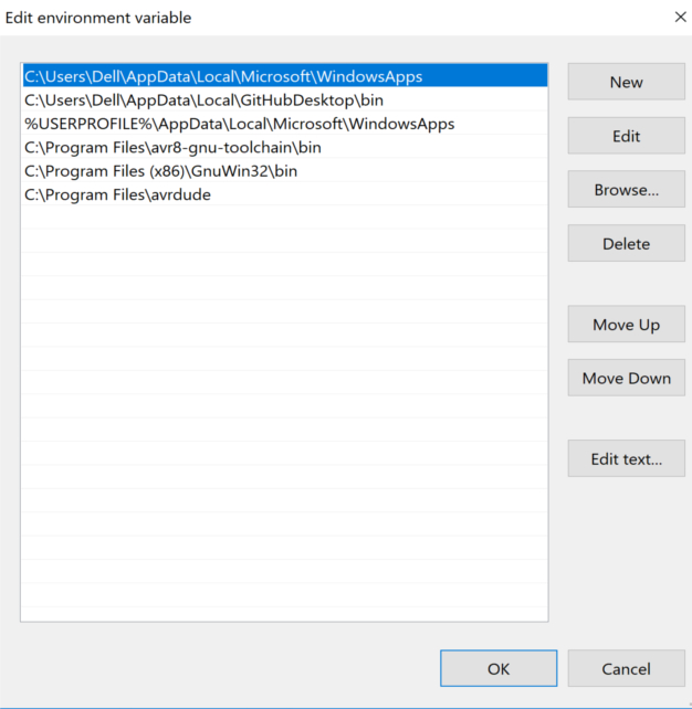
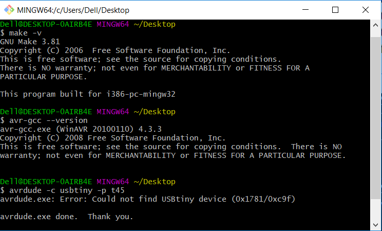
I must type this command Make -v for Gnu make and avr-gcc --version for avr-GCC and avrdude -c usbtiny -p t45 for avrdude to check that you install them and to check the paths.Since I didn't put them I faced a problem but then Wendy asked me are you sure you put them in the same place like the paths so I knew at that moment and I fix it.
Then I change the # in makefile which is in firmware file using brackets because my programmer is usbtiny not avrisp 2. Take it from here #AVRDUDE = avrdude -c usbtiny -p $(DEVICE) # edit this line for your programmer
and put it here
AVRDUDE = avrdude -c avrisp2 -P USB -p $(DEVICE) # edit this line for your programmer
Then I tried to plug the PCB and run zadig as the tutorial says but it doesn't work. But later on I used my FabISP on other weeks such as week 9, week 14.
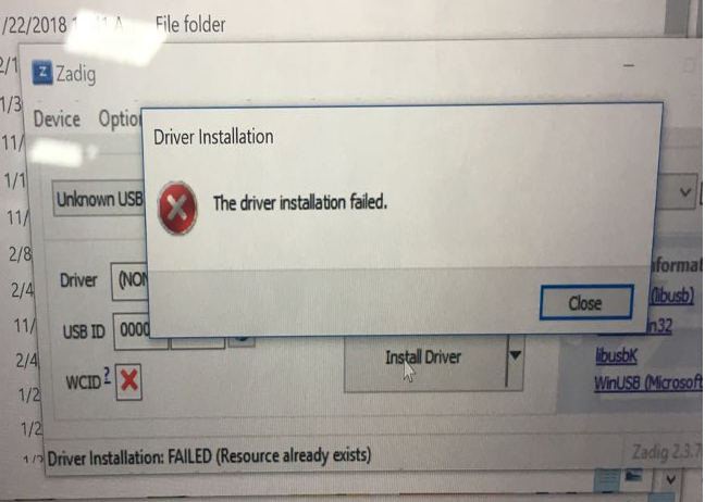
So I checked the connection again I tried to see other students, maybe they face the same problem but I didn't get a clue why this happening so I found out that I didn't download the drivers so I download them but also when I solved this problem the first problem didn't solve.
So Wendy told me to do the board again also I set my mind to not waste time. So I did it again and thanks God I finish soldering fast it didn't take a lot of time.
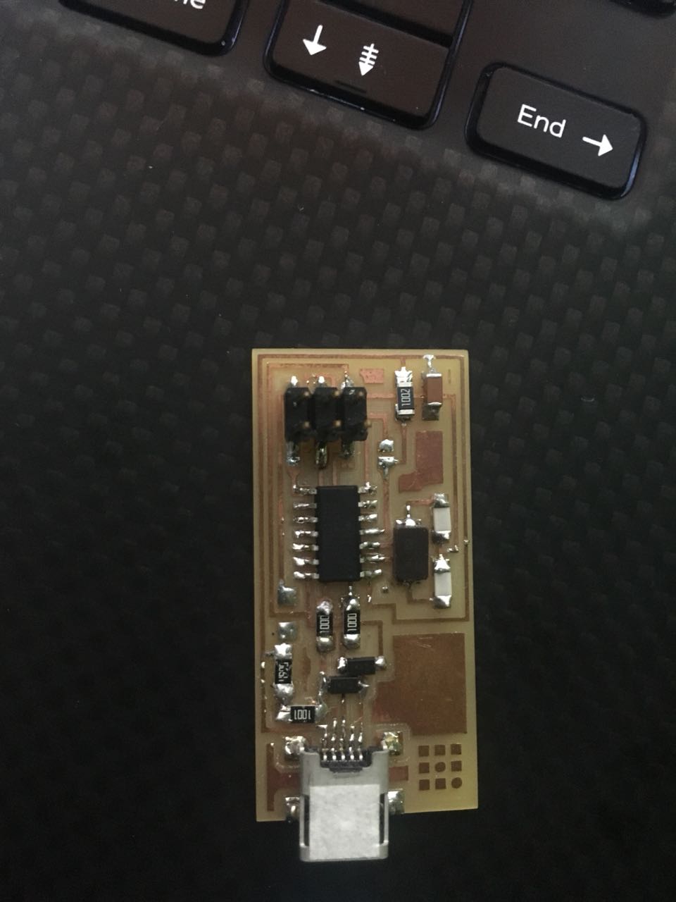
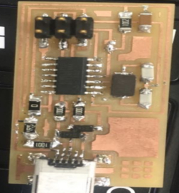
When I finished soldering and checking the connection I notice something that was shocking to me regarding the first PCB. I FORGET to solder the line which I'm pointed at in the image below and I forget to solder the jumper which I made a circle on.
I took it as an experience, the good thing that I made two PCB's and my timing improved. After that, I plugged the PCB also the same problem happen.
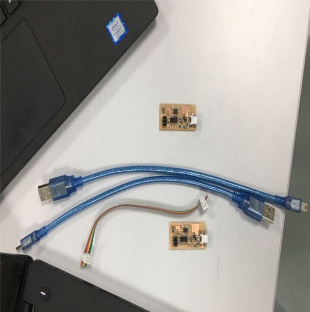
Then my friend Al-Zubair told me to program my programmer by his programmer, so he opens zadig and plugged his programmer to the laptop then he connects his programmer with mine by 2x3 pin header connection and I plugged my programmer to his laptop just as a power source to make it ON. Yes the two PCB must share the same GND
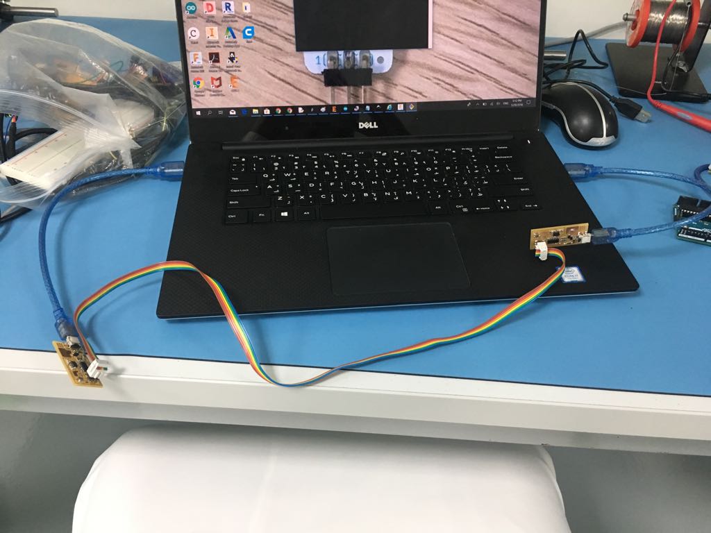
Try not to put the boards on top of the laptop I don't know why but don't put it) I opened the terminal(comand) in (fabISP_mac.0.8.2_firmware) this file you will find it in firmware file. Then I followed these direction tutorial below this title "Program the FabISP (All OS)". I didn't face problems. then to check its working I opened Device manager and I founded fabISP which means its working.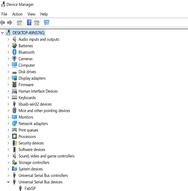
The last step is to remove the jumpers so I can use it as a programmer to program other PCB. Also by removing the jumpers means my programmer will not supply other board that means we must connect other board to any supply such as laptop.
My experince
Since I wasn't here on Wednesday I was afraid to not complete the task on time that thanks god it wasn't that hard maybe the programming part took time. Its the second time for me to build a PCB. The first time was in the college, It was different procedure we used chemical. this way I liked I think its clean and fast not like in the college. Its the first time for me to use a CNC it was interesting I didn’t know that it used to mill the board I thought they will use it just to drill. I found soldering annoying at the beginning but I liked when I found the way that suits me in soldering I think everybody has a way of soldering. Also in testing and visual inspection, I didn't focus which cause to forget to put the jumper in the first board, next time I will make sure to see all of the component or I will make a checklist. In programming, I faced a lot of problems also I forget to download the drivers. which make me think maybe I have a problem with my PCB so I make a new thing but later when I program the old PCB it programmed so that means there was no problem with the board, the problem was with the way of programming I must use a preprogrammed PCB to program mine. It was a really exciting week I showed my friends in college they were shocked, how I make it. Actually every week I show my friends my job they get surprised they think we as a student cant make this. I want to build my own USB. I will build it and I will make a case or cover using the laser cutter.