Electronics Design

What is the assignment ?

In this week we have two assignment as usual the first is group assignment and the other is individual. The group assignment is to use the test equipment in the lab to observe the operation of a microcontroller circuit board. the individual assignment is to redraw the board and edit it by adding button and LED at least. then make it and test it.

The goal’s

My goal is to understand the board and the component also understand and try to finish designing quickly.

In this Page you will find:-

- Introduction

- Design

- Milling

- Soldring

My experience

Introduction

This week we have another PCB board but the difference is we must draw it. In this week I didn’t attend the lecture because its midterms week. So In Monday, I saw the full lecture and in Tuesday I came to the lab to make the board. I didn’t come fully prepared I was facing some issues so Wendy helped to clear the task for me. Neal advises us to see multiple design software. I will now choose Eagle if I have time in the next weeks I will use the others. Not to forget that I used MultiSIM and Multibaord in college but I didn’t understand them well. I took so much time to make the traces I hope eagle is easier.

Design

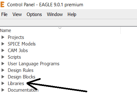
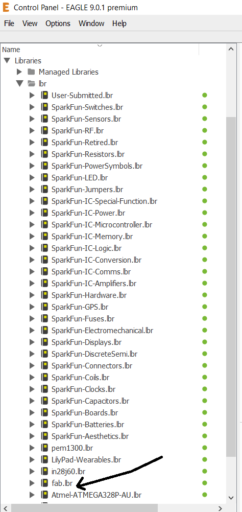
To design like I said above I will use eagle. The first thing is I must add a library. Thanks to Solomon Embafrash I download from his page the library. Since he uses a mac I thought the steps of adding maybe will be different so I searched and I think its the same. So I add the library and this site helped me. I put my library inside Eagle folder in Program Files (x86). After you add the library you just open Eagle and in the main bar at the left side there is the libraries open it and right-click the library that you download and click on use.


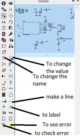
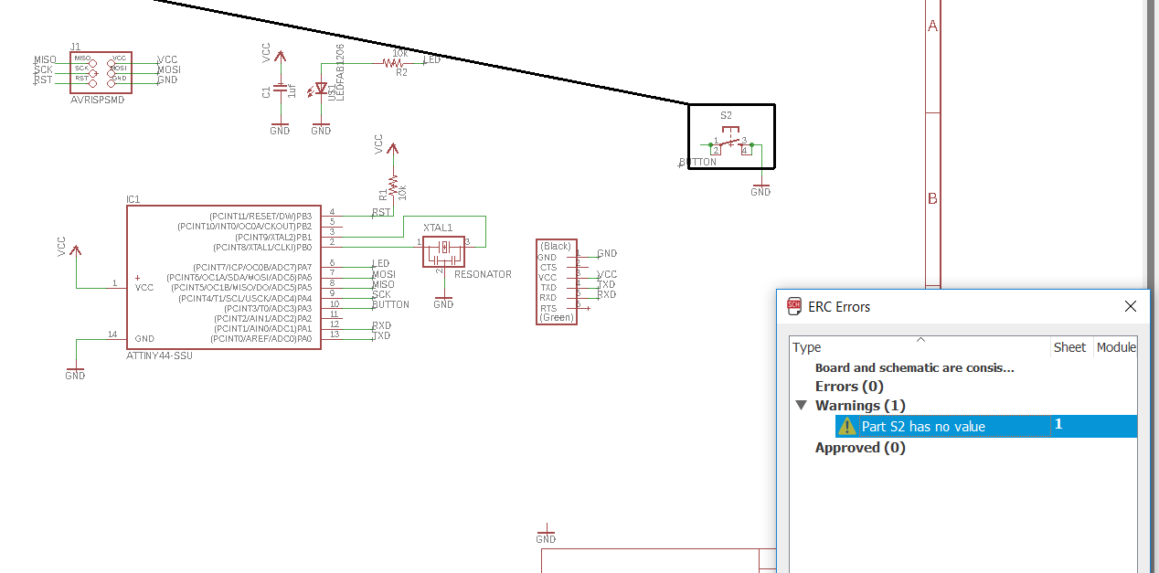
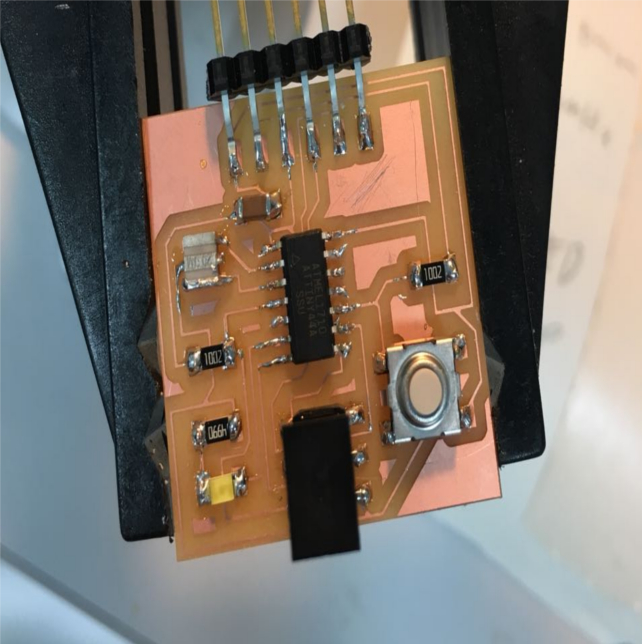
So I added the component that I will use I couldn’t find them from Find bar so I search manually and select them. I decided to add button and LED only and one 10k resistor for the LED to not burn I cloud use 499ohm which will make the LED brighter, but I didn't cause I want to try 10k resistor. Then I connect the wires just by adding small wire to the component then label it. If there is two component that has the same label, the software will understand that they must connect to each other. To do this I added a small line to component then I went to name then I name it then I click on Label and click the line then the name appears. After connecting and changing the names and the values I checked my schematic by clicking on ERC and there was one warning (below) I decided to ignore it because its nor an error and not important to me. After that, I clicked on Switch to board from File.


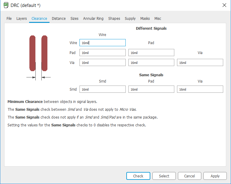
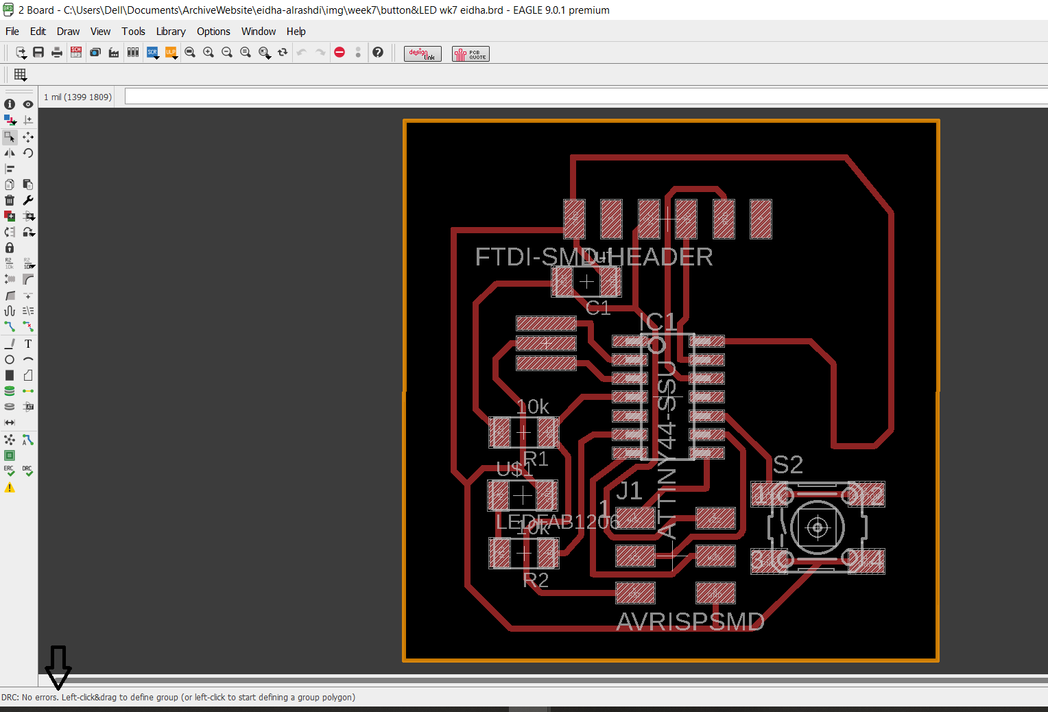
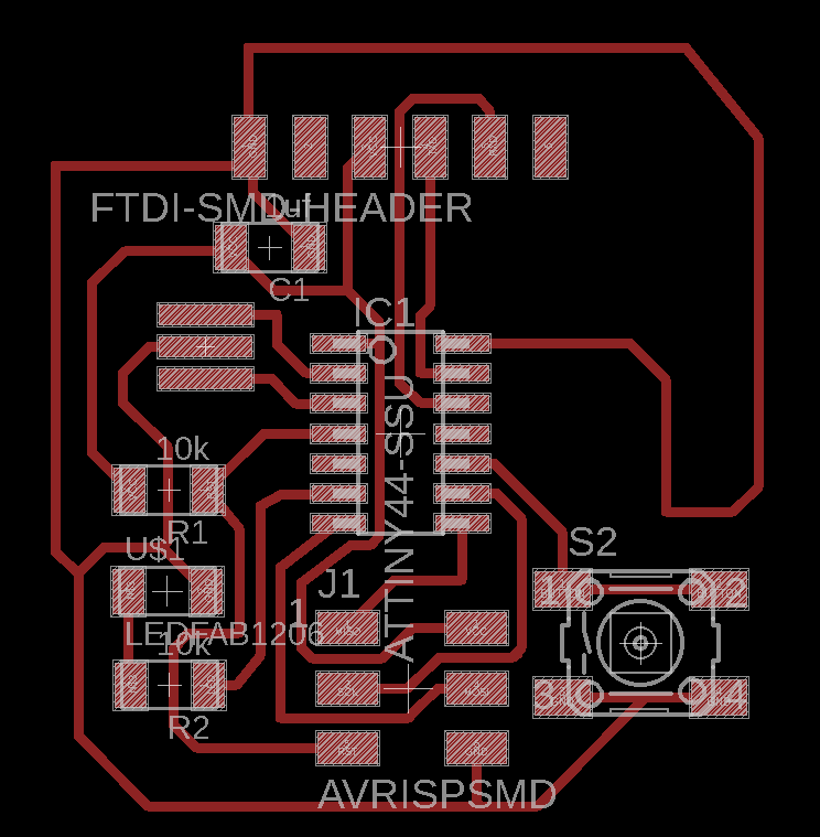
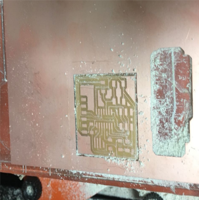
I knew that making the design and the traces will take so much time. I spend 6 hours in two days just to finish this board. I’m happy because I finally make it. I changed my design a lot just because of one trace. It wasn’t easy but I know the next time I will finish it easily. My method of designing was changing the default setting in DRC before connecting the traces this will ensure that when I finish connecting the traces I will not need to move it or change location because all traces that I made and the distance between them depending on the setting so there is no chance for mistake. Now my method of connecting the component is to put the microcontroller in the middle then start with the pins that have one way only. For example, I didn’t start with GND and VCC because they were more than two. Like LED was connected only with pin six from the microcontroller so I start with it. Many time I stuck when I have only one line. But yeah finally I finish it. When I finish my colleges told me that I must check the traces width and the distance between traces etc. After I changed the setting I hide all layers except TOP then I clicked on export then image then I put the resolution 1000 dpi to make it clear when I click on monochrome to make it black and white. I repeated the same step but I showed dimension only and exported it. I took two images now one is the traces and the other is for the outline.


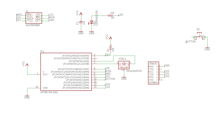
Here is the schematic file
Here is the board file

Here is the tracess as png
Here is the outline

Milling

This process is easy because we already did it in week 5. I opened fabmodules then open the image and choose 1/64. I set up the CNC then start milling. When the CNC finished milling I notice that the traces despair first thing came to my mind was the traces were very thin. Then Carl told me: dude you are using 1/32 bit:). Thank God there was no problem with the design. So I changed the bit when I start it again. When I finished there was copper layer the CNC didn't take it so I changed the depth from fabmodules to 0.15 and it works. After that, I opened the other image (for the outline) and set the Z. When I finish the board, I looked for short circuit there wasn't any short circuit.


Soldering

I collect the component then I start soldering. It took some time but not like the first time. I finish with soldering then I visually inspect the board also I tested looking for short circuit I already expla ine this in week5. But there weren’t problems with the board.


You can see I used 499 resistor on the board because later on, I changed my mind to make it later( mention ohm lows with calculation).


In this week I didnt tested by a code but in week 9 I did.

Oscilloscope

First here is a good link about Oscilloscope that hashim gave me Hashim teach me how to use the Oscilloscope and power supply. So first I used the power supply. Then I change the voltage to 5V because this what the board gets usually and then I connect the clips of the power supply on the board. The VCC to VCC and GND to GND. So I when I connected, the current was 0.01A so to get the power it's easy the equation is P=V*I where the P is power, V is voltage, and I is current. So the V=5 and I get the I=0.01 so the power will be 0.05 watt

Then I moved to Oscilloscope, I learned how to see the wave and move it up and down(4) also how to shift it right and left (2) and how to decrease or increase the peak to peak(pk-pk)(3) to be able to see the wave this is manually but I can click on Autoset(1) to set the wave. So the first thing I connect the GND to GND then I connect the VCC to the LED on the board to see the waves. ALready the board programmed to blink and the delay 10ms.


As I said I connect the measuring probe to the LED on the board and I set the attenuation to 10X just to see what will be shown on the screen.

Below you will see the frequency I get which was 46.38HZ. Each square is 100mv so when we count vertically we will get 5 squares which means its 500mv.


When I changed the attenuation to 1X you can see bellow the frequency changed to 9.3HZ.

My experience

Designing a board wasn’t easy. But it's a good experience to design and know how the circuit builds also the component and what is their function.now I see building a board is not hard and I'm sure after two weeks it will be easier for me. Designing is not impossible but not easy. This week I started late because of the midterms also next week I will travel for a week so I must finish here quickly to not miss a lot.

Previous week Home Next week