Aim:
To unerstand the working of output devices
Basically this was assigned to test how do the boards that we designed function, to the commands that we feed them through..
For this we had to make a controller board and a driver board, which would function according to the instructions guided by the controller.
Task 1:
Points to be considered before designing the board for any output device.
Basically there are many essential considerations to be made before you actually design the board.
Some of them are listed below:-
- The first thing to be decided is basically the power consumption by the device that you use, because it is resposible for the track width that you choose and also the power regulating components that you might need, along with few other connection parameters to be taken into consideration.
- The track width of the tracs that are to be milled,
This does not matter much when you have a power supply upto 12V and current of 1A, but as they go on increasing the regulating components to protect the circuit and the track width matters upto a certain limit, to avoid damage to the components.. - The components for regulating the power supply, if dealing with AC or DC currents, or even in the conversion of them.
- The provision for removal of excess heat, produced by certain components, such as mosfets, to avoid the damage to the respective components and even the tracks.
- ANd few others like these play a very crucial role when you design output circuits
Considering all the above we can design a board for any output devices that we need, most of em could be found here..
Task 2:
Desiging of the board
This process I had actually thought to be considerably simpler refering to the processes I tried before,
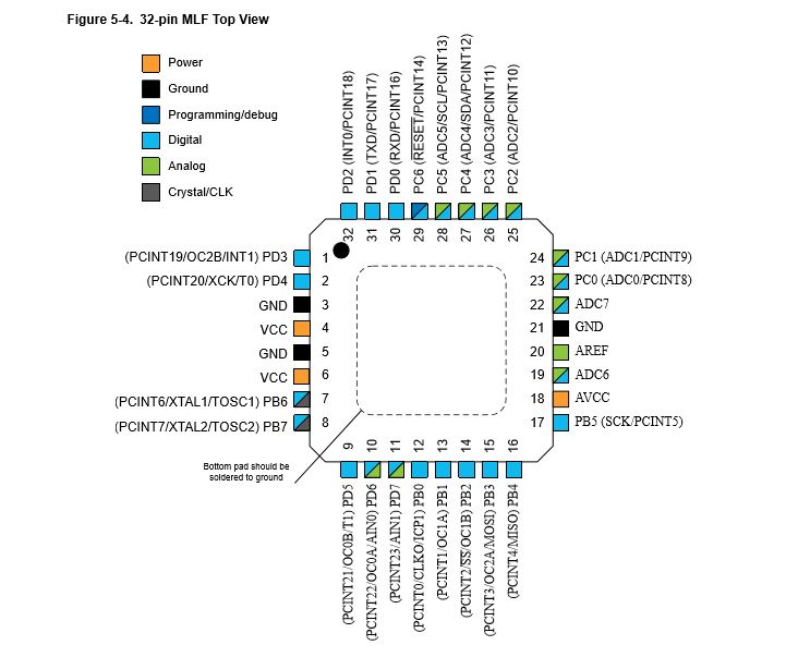
Hence I started to design the schematic, starting with the things an IC would require to function, and then added the components, what I need for the out put.
For this task I had planned to develop the board for my final project because my project had a lot of output devices hence I had decided to test every port possible for it's working so that I could ensure maximum efficiency for my final project.
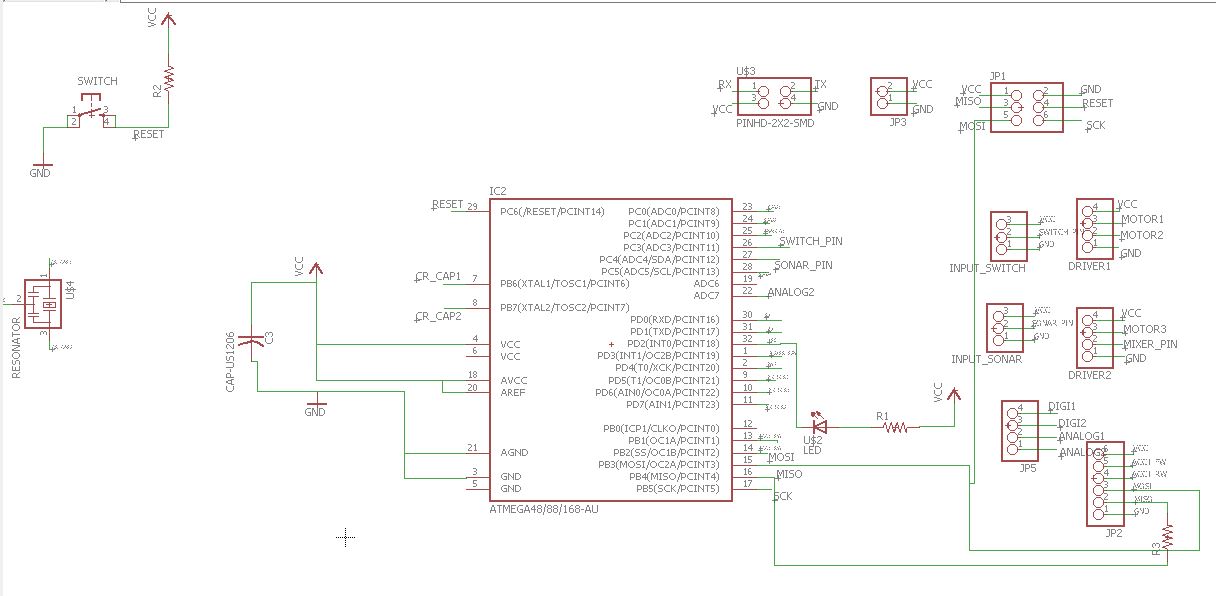
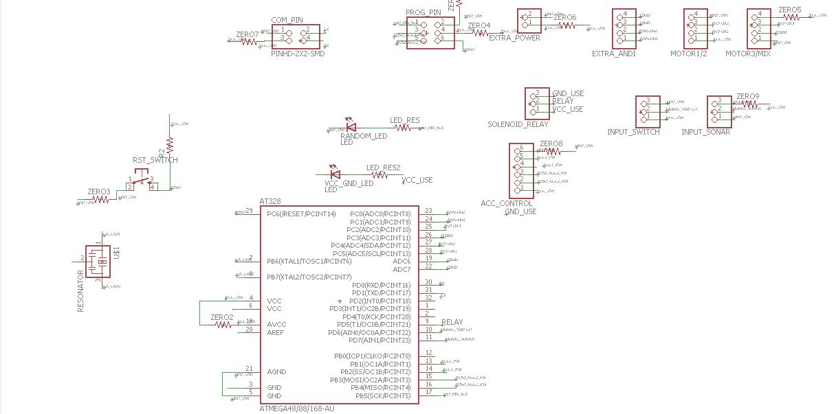
After a few efforts and correction I had got a schematic that looked like this..
The Problem
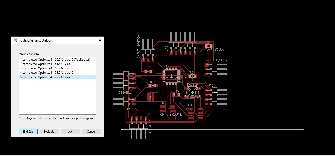
This was a great perfect schematic, but the only case was when I went to rout the thing i had became difficult like anything, like for 2 complete days I had found no answers for auto rout.
There was always a single or few connections that would cause a mess.
Solution
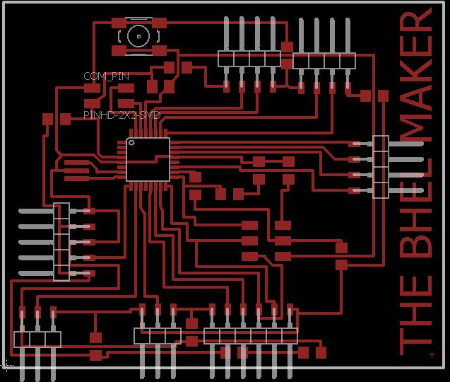
For this I did not find a specific solution for the same schematic, so what I did was kept the schematic same as it was and prepared a new one.
This time what I did was I just imported the components
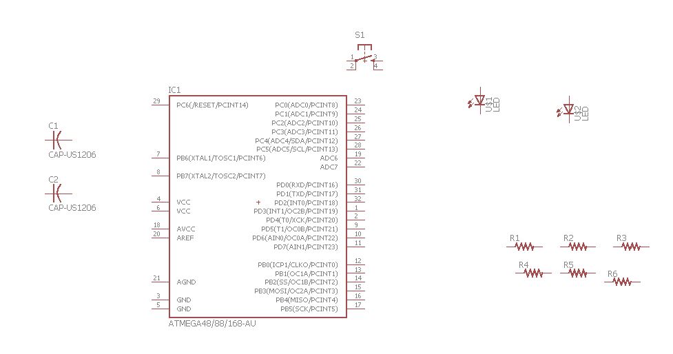
and the manually arranged all of them , and then with the help of wire tool in the board section I generated a random (logical) circuit, refering the inputs and outputs needed(ANalog or Digital), seeing the routing of of power pins (VCC and GND), all from the data sheet.
This turned favourble because I was able to arrange the board according to the need I had to make the board easy for milling.
Then i drew the schematic as per the connections just to ensure that all the connection I made were fine also the defined advantage of schematic is it's easy to debug and understand the circuit. Hence following was the circuit I was able to draw and verify..
Task 3:
Milling the board
This as expected was again supposed to be an easy task, but as usual it had also bugs too.
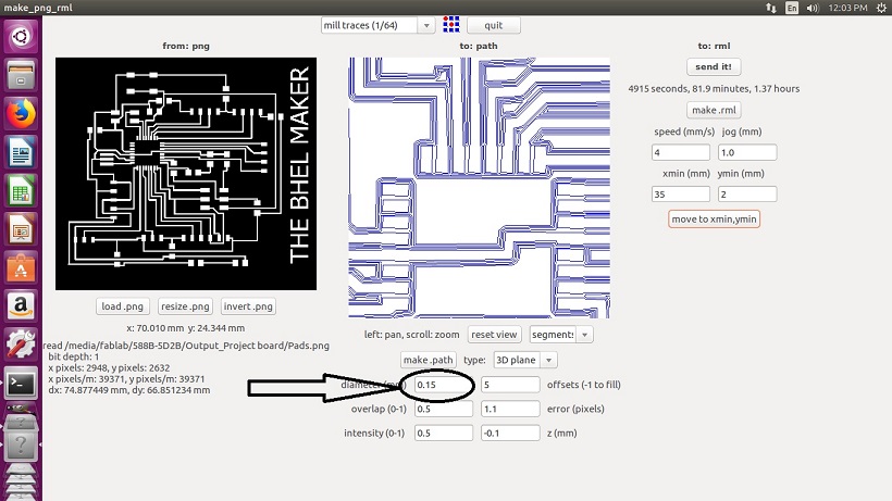
Initially when I went to mill the board I had this result on loading it on the Fab module,
The bit that we had was 0.4mm (1/64"), now the case was the bit was unable to mill the tracks of the IC, as seen above,
For this I tired to play with the diameter of the tool and manipulate it till it mills the tracks..
Cause the diameter defined the tool ofset I was able to get an image as seen here, due to the logic stated below..
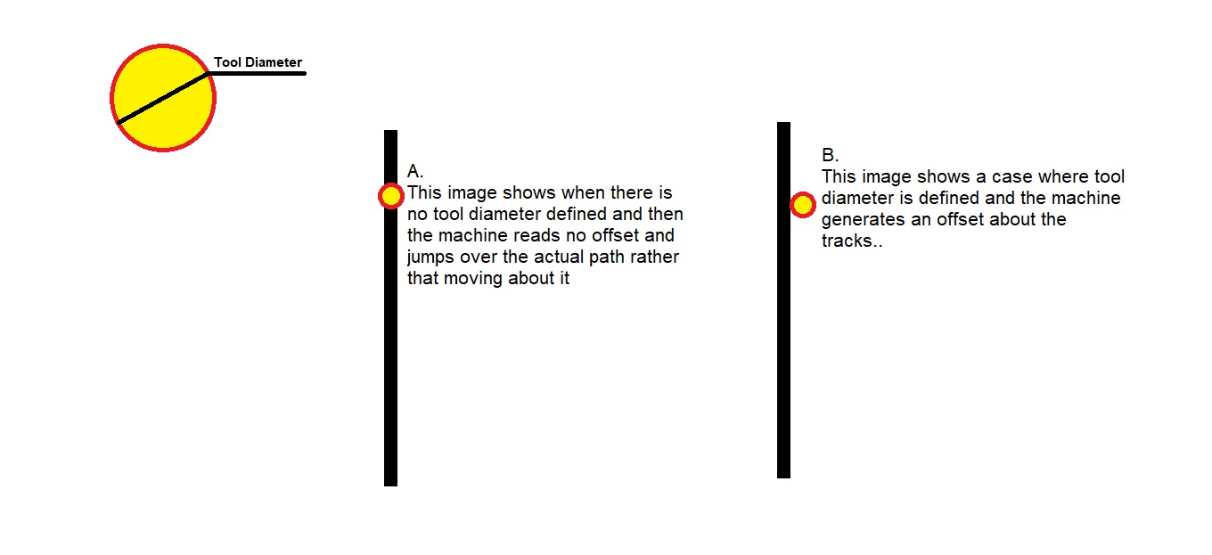
But the case was when I played with the diameter to get the IC perfect I had lost the control over the width of the track and then I had got a funny board as this one..
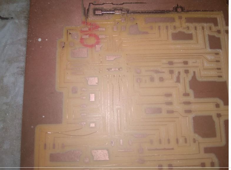
Later without much of deep research I went to mill the other one reducing the offset, but the only thing I got was less joined tracks, as seen in the image below...
This was also a fail, then the next step I decided to take was to mill the same board with a heigher ofset, but with a V bit
The result that I had got was as seen here...
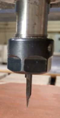
During the process I had also broken a couple of bits, this was due to the board I had chosen to mill, was hard which broke the bits as the dashed it,

Now the case had been out of hand and I had been extremly frustrated....untill I got the way to solve my way out.
Task 4:
Process of the Solution
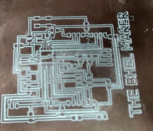
For this I had consulted few of the instructors and I had got this image as a referance for analysis..

Here the image shown was milled using a bit of 0.4mm (1/64"),
Here I realised that somehow the track width and the width of the pads was found to be equal, but as logic suggested the there was no specific point in icreasing the track width to that of the pads, Hence there was something to be done to change the width of the pads of the IC and customise it as I need, by actually rendering the library..
(Till then I had not realised there was a processor defined in the fab library..)
After a runthrough in few tutorials I was able to run throgh the process as defined below.
Procedure to the Solution
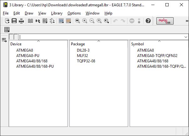
- The initial step is to open the respective library in the open command of the library section.
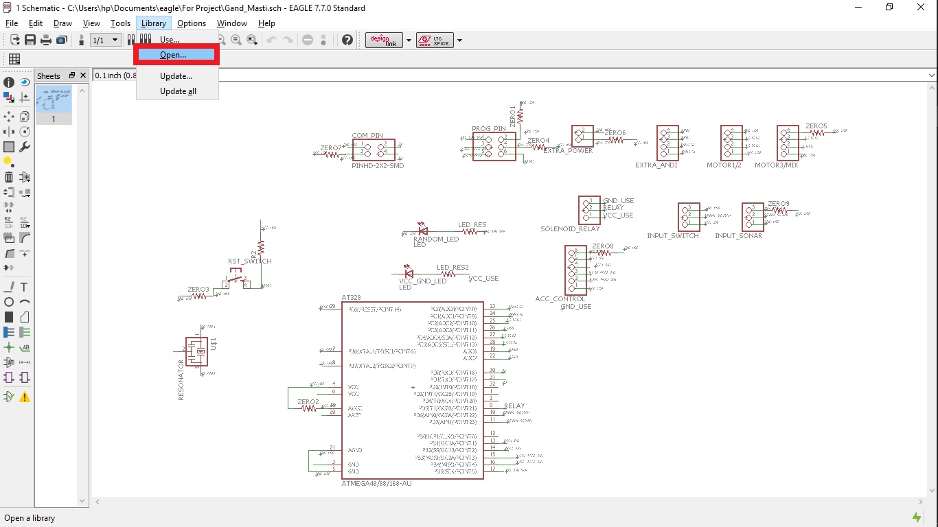
Where you navigate your way to the library and open it to find something like this..
- Here you define and select the package that you have to edit
{NOTE:- Select only the package in the package list rest other things are vain to deal with}

Once you select it, you open a window as seen above, this is the menu for package editor, in my case this was the library I had for my IC., and the package was "TQPf32-08". - Here you enter a command as "change smd", which opens a panel for you as seen here, this displays a range of standard track widths,
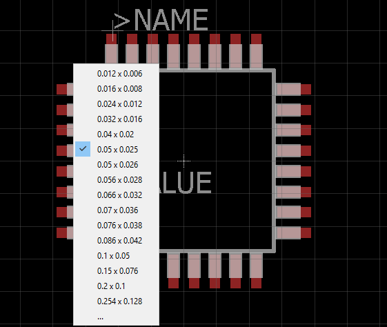
Here you can either select one of the standards given or there is a options as "..." , at the end of the list, this opens a terminal as seen here, where you can specify the parameters you like..
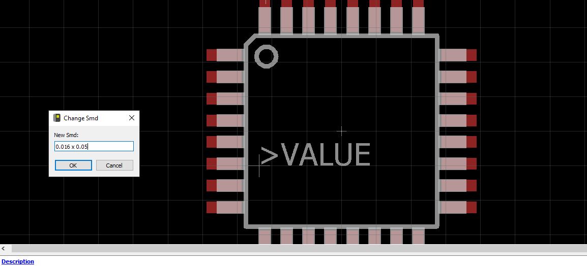
Here you enter the numbers refering the format shown in the standard list, i.e {(0.xyz) x (0.abc)}.
Then hit enter and select each and every pad to notice the change.. - But there is a catch which is to be noted that the dimensions that you enter for horizontal pads need to be reversed for the vertical pads, for obvious logical reasons..
For exampls:-
Horizontal: {(0.xyz) x (0.abc)}
Vertical: {(0.abc) x (0.xyz)} - This command changes the library forever, but now the case is it only would be applied to the pacakege you add now on after changing, but what about the existing package,...For that you use the "add" commanad and make an attempt to add the same package of the IC in the schematic, which gives you a warning as seen..
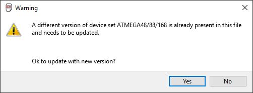
This confirms that the changes have been applied to the library that you had edited.
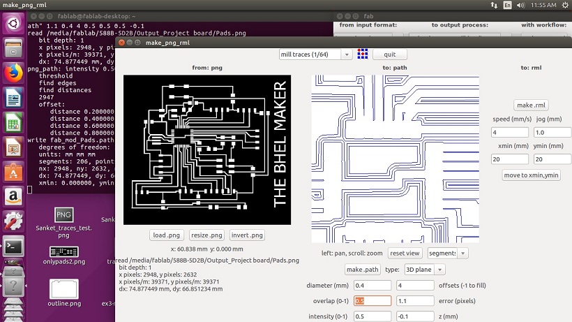
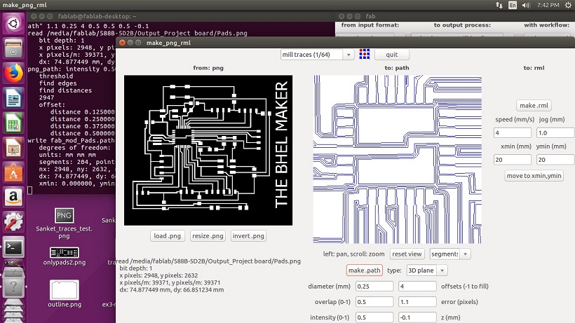
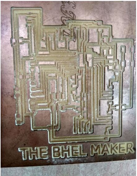
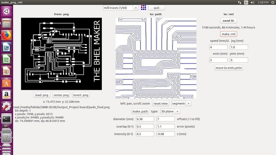
After this when I had loaded my PNG to fab module I had following image for the path, still for a safer side I had kept the offset as 0.33 rather than 0.4,
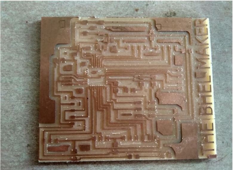
and I had got the board milled as seen here..
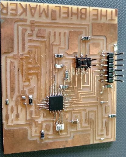
Which I had soldered with not much of an issue, but with great help of my instructors, for soldering such small tips, and had got this as my final soldered board..