Aim:
To learn and understand the processes and laws about designing electronics
Task 1:
The processes before actual designing
Before designing the a particular circuit there are few procedures that are to be followed in order to avoid mess during the design..
Some of the considerations are listed below
- First you need to decide the purpose and then the required components for the desing{Considering design for my project's board}
- The next task is to decide an appropriate tool for design, considering your level of knowledge and familiarity, {For this I chose eagle, since it has a bit of user friendly interface...
You can download it from here} - And the you need to configure your software and start designing the PCB
During installation of eagle there was a major problem I had encountered....
The issue was not about intallation, it went fairly well, the issue was about configuring the libraries, I actually tried a lot of different ways to install the "fab.lbr" library, but it didn't reflect the in the add command, untill I treid and found this method that can be easily and universally applied..
- First create a new scematic in your project
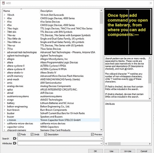
- Then enter "add" command into the command box to open a dialogue shown below
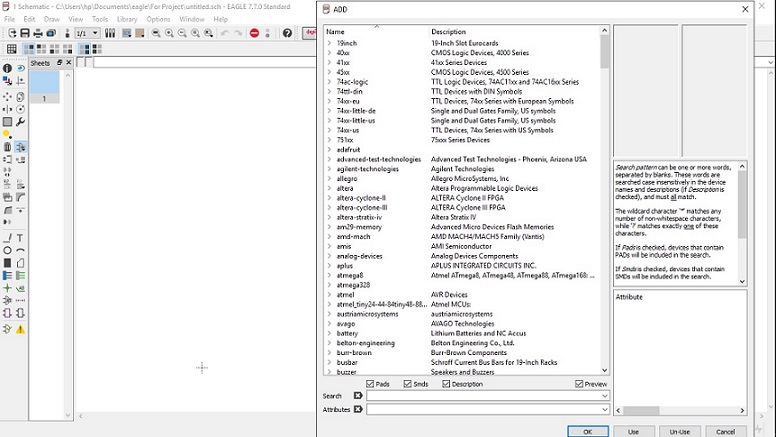
- Then hit the use button on the dialogue box and navigate your way to the folder containing the library
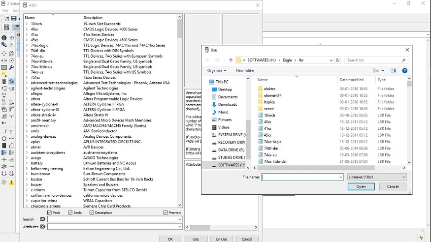
- Once you hit open, the library gets added to the stock and then you can directly use them into the editing.
Task 2:
Understanding interface and commands of Eagle
This software as said before has a very generic user interface, which if explained even a bit, can be commanded by a beginner(as of me).
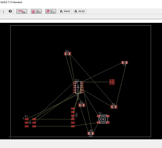
This software basically has two modes(which I figured, and solved my purpose through the assignment), between which there is a switch that navigates you through the modes, as shown in the image
A. Schematic:- Here you design the basic circuit of your board, in terms of wires and compoents
B. Board:- Here you can actually arrange the board in terms of milling tracks, routing them perfectly
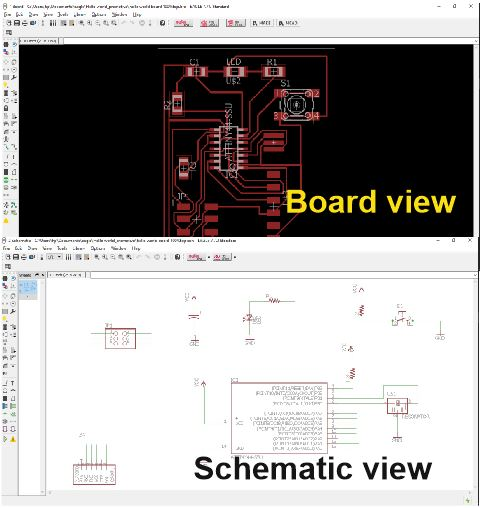
After this the most important thins is to learn with the commands in both the mods with images that show you the output of each of them..
Hence considering the above parameters it gets you prepared to design your desired circuit.
Task 3:
Designing the echo Hello World board
The initial step is to be familier with the data sheet, this is basically a user manual for the micro processor. The data sheet of a usual processor is very long(400+ pages) and tiresome to read, for this it's quite necessary to understand and consider what to read and what all you can skip at a premitive level.
The points you need to consider are the orientation of the controller, the alotment of the pins for a desired input and output, numbers of the basic programmable pins, the power needed to power the PCB, and details about the pins.
Sub Task:-To understand the concept of hello world board.
The basic concept of the hello world board is to selct a micro controller, join the components in such a way that you ca program the controller, and the add an LED with a resistor to check the results of the program.
The components needed to initiate processing of this micro controller are listed below..
- A capasitor of 1 micro fahrad
- A resistor of 499 ohms across the LED(so you don't burn it out)
- Two resistors 10K ohm each across the Button and Reset respectively
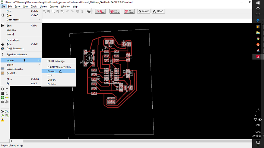
- A resonator of 20 mHz
- An LED
- Pin headers
- A switch
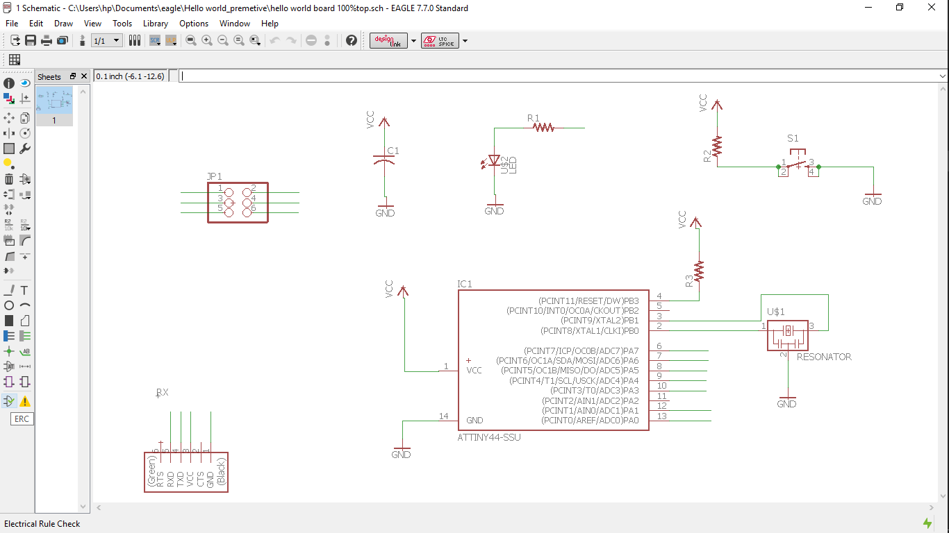
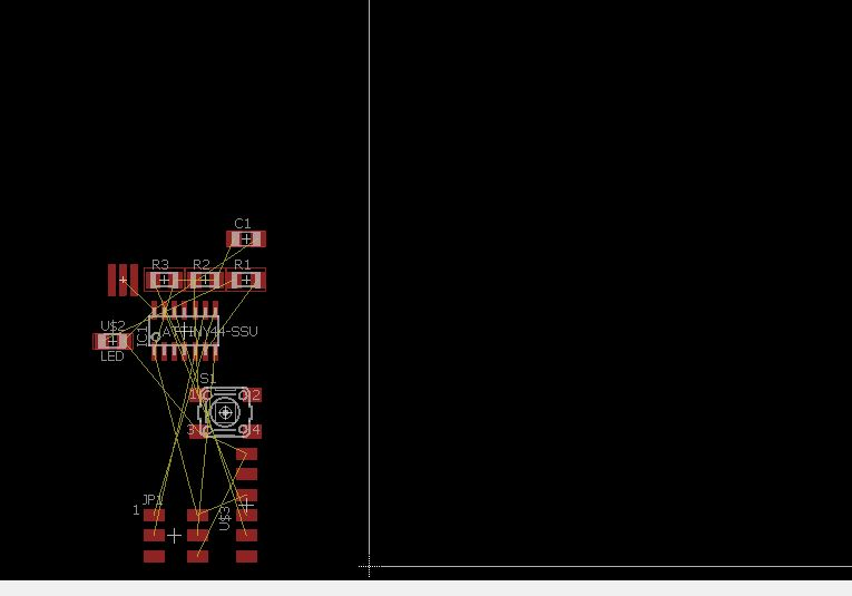
Considering with the components we can generate a schematic which looks as follows
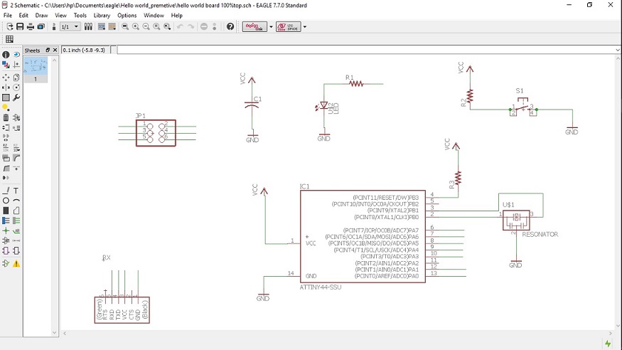
For this i used all the commands that are described above, in oder to add, move, wire, and delete the components respectively.
Problems faced and solutions
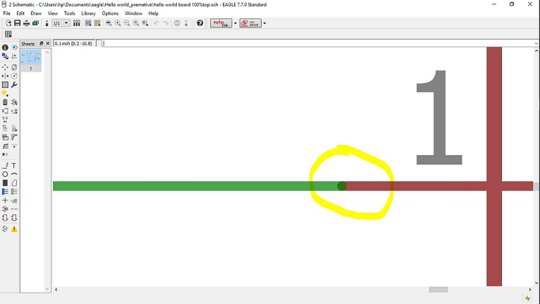
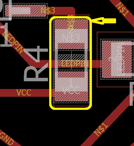
1. There was a basic issue with my design about routing the wires, about how its done, I had routed the cables perfectly yet it didn't show as it was connected, they looked something like this.
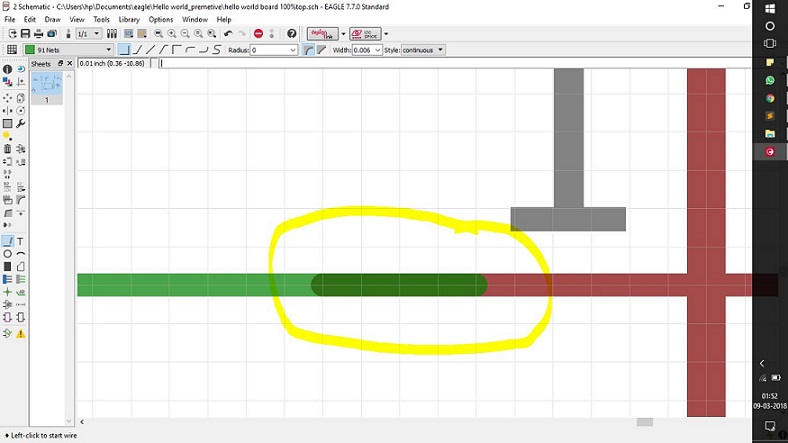
After a bit of debugging i came to know that the wires i had joint were not actually junction to junction which resembeld a wire cross, and not a connected end.. Hence i solved it by re-routing the wires with a joint that appeared like this..
2. Then the next issue I faced was about the confussion in the cluster of wires.
Initially i had a schematic that looked like this ..
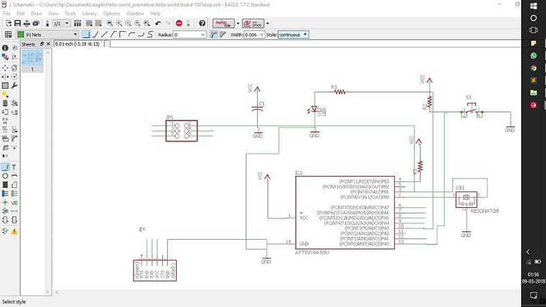
It was a total mess of wires which didn't explain which connection was a cross over or a joint.
For this i later found a solution of naming the wires,its basically if you name two wires same they would be joint
For this you right click a particular wire, select the name option.
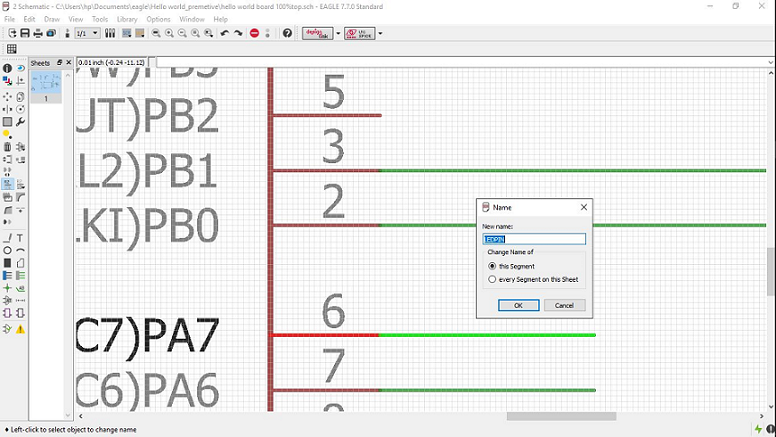
Once you name the wire, go and name the other wire with same name, and a dialouge pops up as shown below
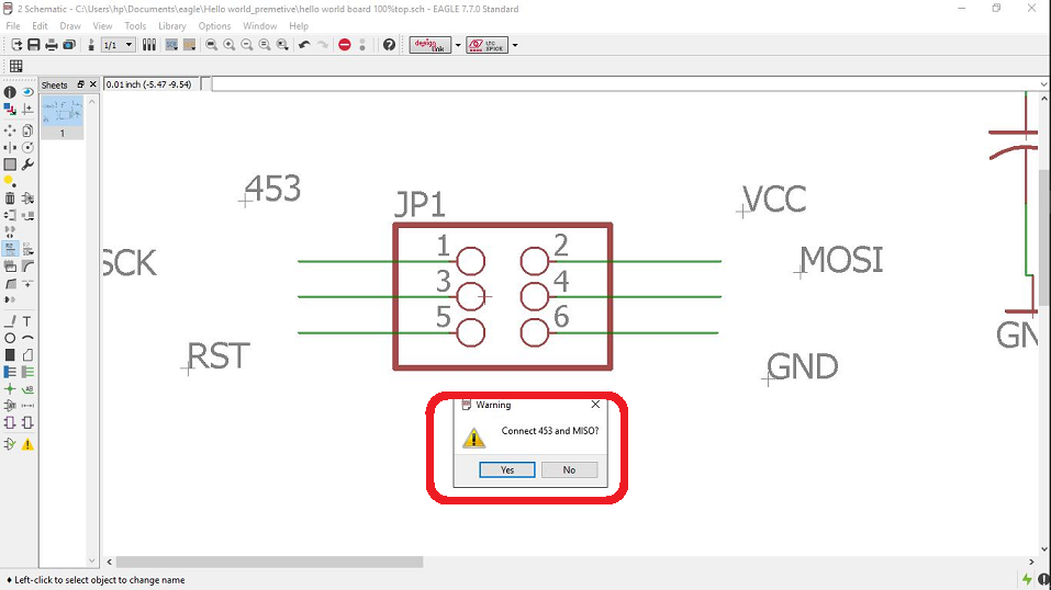
Hit the yes button to join the wires, finally after doint this for the entire board, the sketch displayed previously was the final clean schematic that I had got..
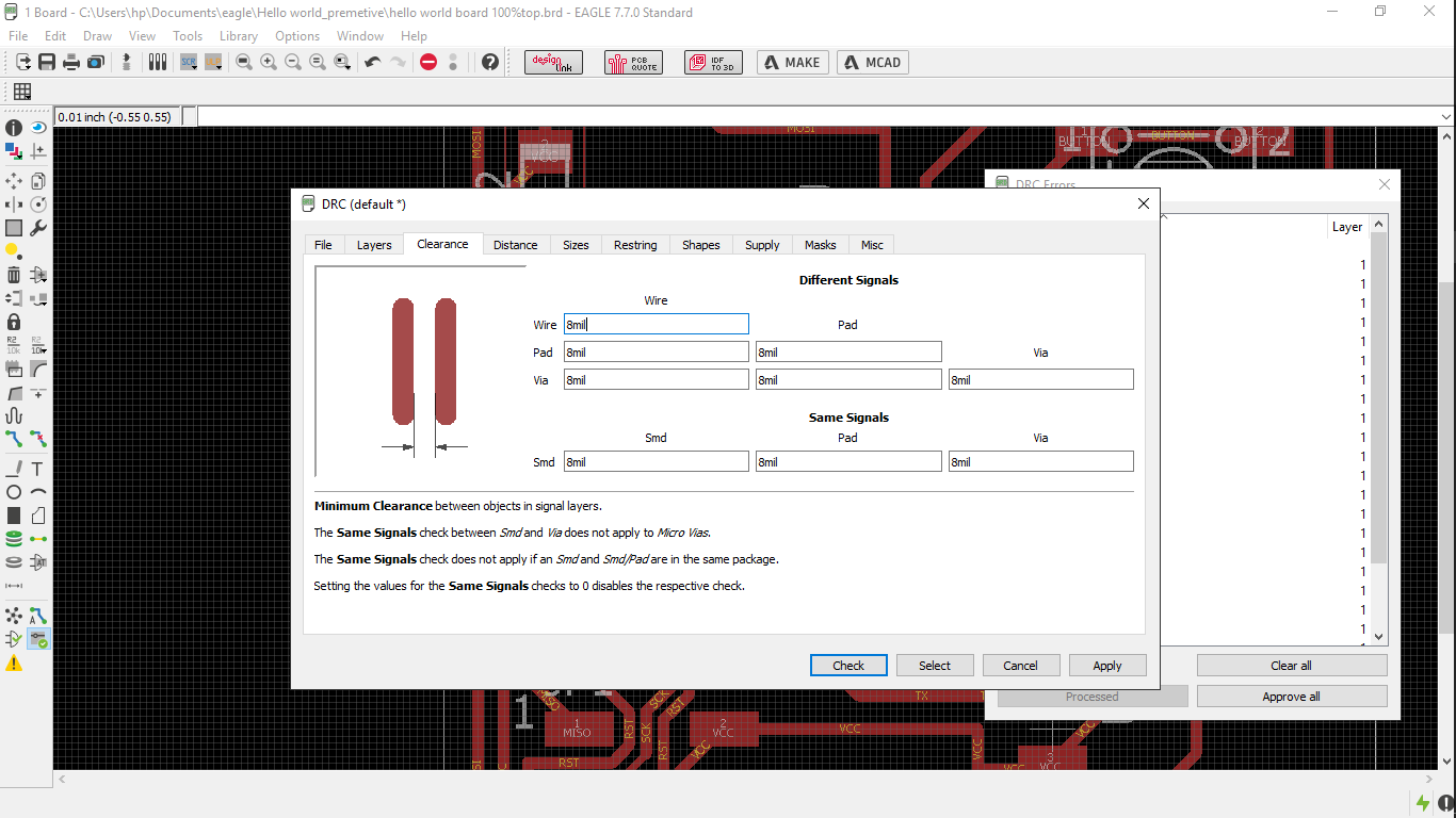
Sub Task:-Checking the electronic rules.
This is done with the function named as ERC(electronic rule check), here basically a program checks for the open wires or non connected connections, or even wires that have no been routed neatly
I ran the scan on my board for which i got a few warnings,
Initially i was scared about so many warnings but finally realised that these were not errors but rather warnings which displayed there were no lables for the given circuits
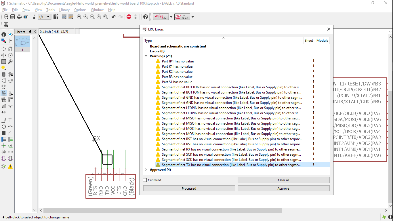
Hence i approved all the warings since they ware not errors that could hinder with the functions of the working of the board.
Sub Task:-To arrange the board in a format suitable for milling.
For this you just press the switch to board button to find a window like this..
Initially you get the direct routing of the scematic, where you see the pads and the values of the components and then the cluster of wired connection that show the connections in the schematic
{Note:- The changes made in the schematics are appkied to the board in real time}
For this the initial step is arranging the components into the board space, which you do with the move command
Initially while doing this step you arrange the board in an arbitary manner, just by keeping in mind a few key points, those being..
1.The controller always should be in the middle
2.The pin headers should be at the edges, to make the fixing of the pins easier
3.etc.
etc
These are rather necessary for the ergonomy of the board.
Further you can begin routing the board, that is setting up the path for milling.
For this there are two choices
A. Manual routing, where you drag each and every route to join the circuit
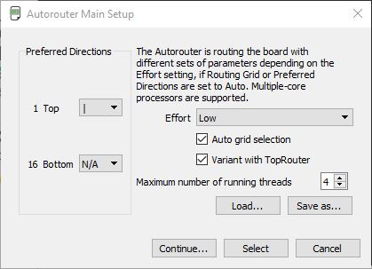
B. Auto routing where you let an algorithm route for you
Once you click for auto routing following is the panel where you specify the parameters and below it are the results that are displayed at the end of it
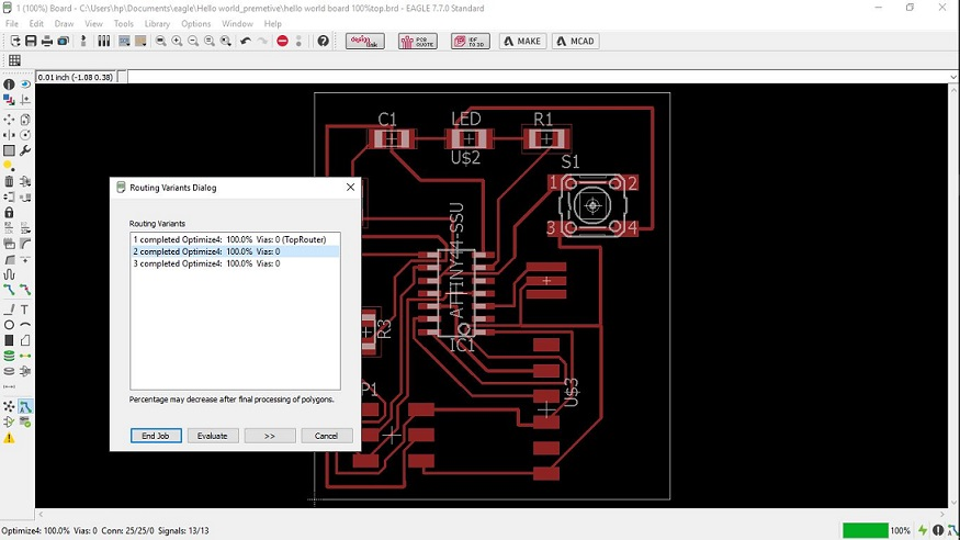
Hence you can get your board routed in the suitable format..
The only issue with auto routing is it uses a track width of 0.010 inches(10mil), considering that it routs the entire board, hence the tracks are routed too close.
For this I had to re rout the tracs, using the preferd track width of 0.016 inches(16mil), it's also prefered to use the width of 0.020 inches.
Problems faced and solutions
During this process there were many problems that i faced some of them are listed below, with the solutions..
- The initial issue was with the routing, the case was there was every component going to the VCC or GND ports individually, as seen in the image below, this makes it difficult to route perfectly
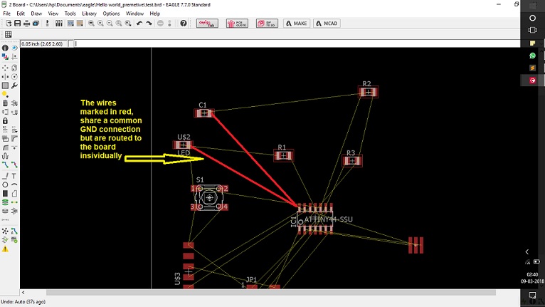
Solution:- For issues like this there is a key named as rats nest, it has a dedicated function of grouping the connections which have a common destination which makes it easy to route
For example, if VCC of pin header and LED go individually to the IC, then by rats nest the go through each other and then to the IC, through a common route, which makes the ciruit look simpler
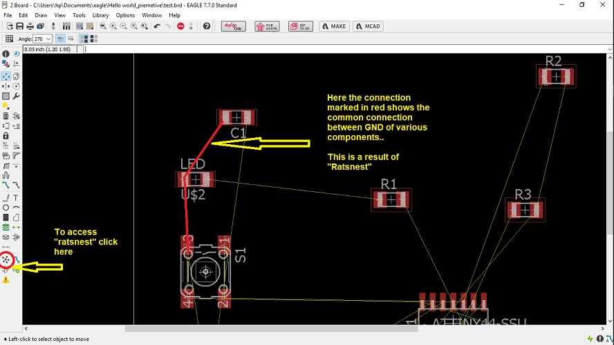
{Note:- In order to manipulate the changes done with rats nest its must to analyse the circuit initially} - The next problem was with the track orrientation and width:-
The issue that auto routing creates is it makes tracks too close to each other without any consideration about the tool diameter, so the issue is the tool dosent cut the path properly or rather it joins all the close tracks and then you'll have to remove the tracks manually
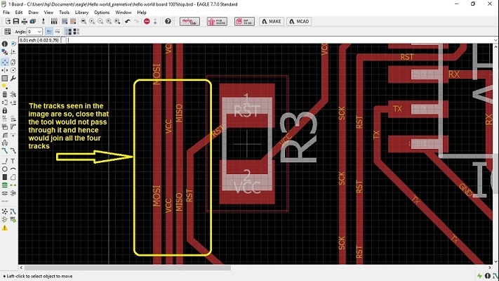
Solution:- The solution for this is initially print your circuit on a normal paper 1:1 scale, figure out the difficult parts for joints, and repair them by ripping off the exisiting tracks and generating new with a bigger space between two tracks - The next was not actually a problem, but some skills to be learnt or can be said a temporary adjusstment to be made (Jugad)
Basically the case was, there was a wire which was not being routed, as seen below.
So for that what i did was added a pad for resistor where i decided to put up a 0 ohm resistor, this created a jumper connection...
Sub Task:-Checking the Design rules.
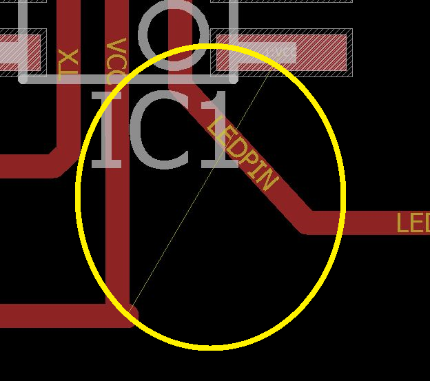
This segment is basically cross analysing the circuit using a simulator, which uses its paremeters(that you feed as a real time data)
, to verify the circuit. This is done by an inbuilt program named as DRC(Design Rule Check).
Following window guides you through the layout of the function...
Initially i didn't much realise the function so initially i just went through all the commands using arbitary parameters and checked my board I didn't get any errors
Later I applied few extra parameters to just see the function, like changing the path size, required tool size
And got the results as following..
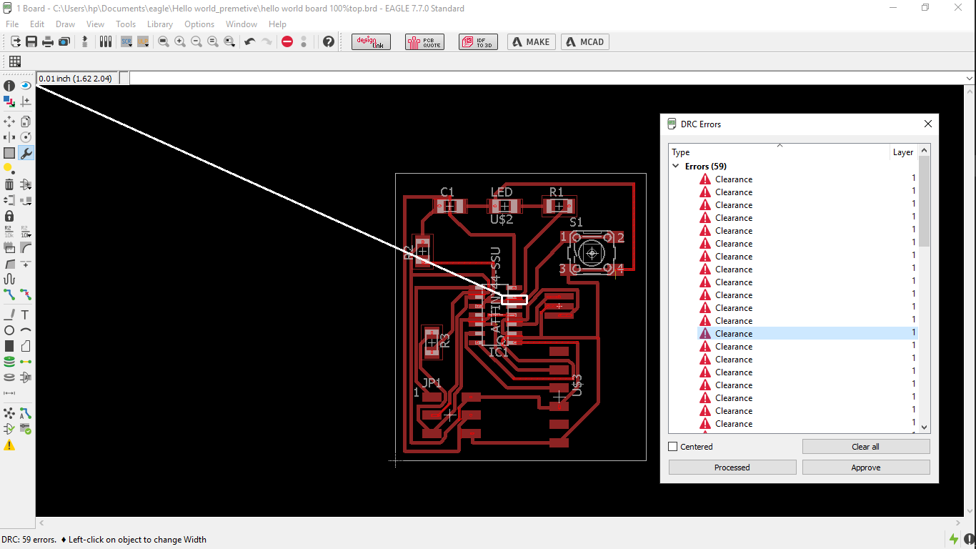
The errors are at the junction points where the tool (parameter provided), wont physically be able to cut.
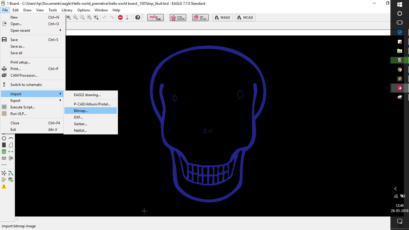
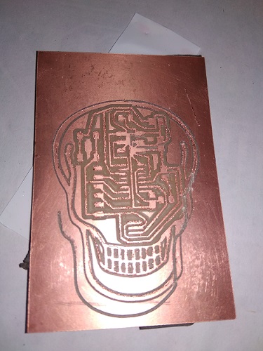
After the design of the board I wanted to rout the entire board into a skull, for this I generated a bitmap of skull in corel draw, defining the size that I needed.
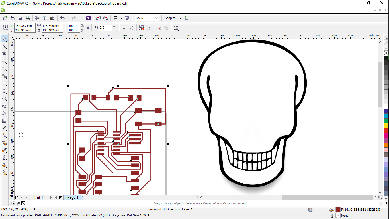
This I had generated by auto tracing the image from one of my logos, and had deleted all the other segments and cleared the space for routing the board.

This I exported as bitmap through corel
which I imported into eagle(it supports the format of *.bmp),
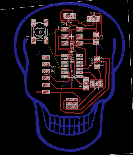
After which I re-arranged the circuit according to the need of the skull and routed it to get the following, the circuit was routed in the eagle itself, that made it easy for me rather than arranging it in the corel draw.

Considering all the issues and i milled the PCB which looked like following..
After the assembly of components it looked like this..
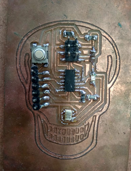
The issue here was I didn't cut the PCB using a bigger it and had kept it be as it is, this was because the border file that I was trying to upload was not being set to the same origin as the initial traces,
and hence it had given me an abrupt cut as seen here, considering which I prefered not to cut the board, the other time..
Conclusions
The Board went quite good in terms of design.
There were issues when I printed the board, I was unable to cut the bourndary, because the design or the machine had left the origin,for one of my board, therefore I decided to keep the board as it is.
Also here I exoerienced a bit of problem while soldering, since this was one of my initial boards, but had decided to make sure that the rest of my boards would have a better and cleaner solder.
Task 4:
Group Assignment
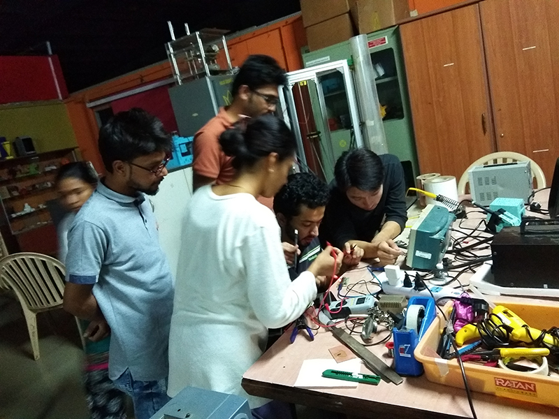
The group assigment for this week was to check various tools, which display numerous properties about electrical components.
The components we have in our lab, and their functioning goes as follows:-
- Oscilloscope:-
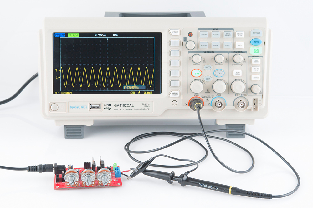
This is an instrument used to see the flow of current in the form of waves over a display which shows waves as a relation between potential difference Vs Time. For this we had tested a hellow world board, designed by one of us, and had achieved the results as seen..
For this the setup we had was a laptop, connected to the helloworld board, where the ocilloscope was connected to the communication pins of the board, and the board was connected via a programmer to the PC, and we were to measure the signals of any particular pin that was connected with the oscilloscope.
For the initial we were quite guided by one of our colleague, Rutvij Pathak, and one of our instructors, who being electroninc engineers had previous experience with the tools.
The wave is actually supposed to be in the form of pulses, but rather it appears to be sinusoidal, it's because the soldering was not perfect on the position where the oscillator was attached.
- Multimeter:-
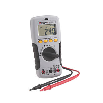
This is a device probably available in every lab it has mutiple function as the image describes..
We used it to check the polarities of the LED, ressitance and capacitance and the continuity of the circuit board
Task 5:
Loading the test program in the hello world board
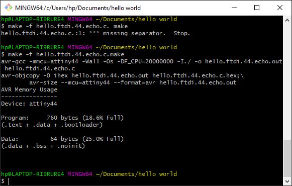
For this assignment we had to load a test program written in C and Python, on our hello world board and test it.
Following listed were the commands we used to copy the program to the board.
- Initially to cheack weather if your bboard is detected you type, "lsusb" in the terminal
- Then you download the test code from the link described here
- The next task is very crucial, the micro controller does not understan C or any programming language, for which we need to convert our program to HEX file and then load it..
For this we type in the command "make -f 'name of the file.c(hello.ftdi.44.echo.c.make)' " to convert the files to HEX which can be then added..
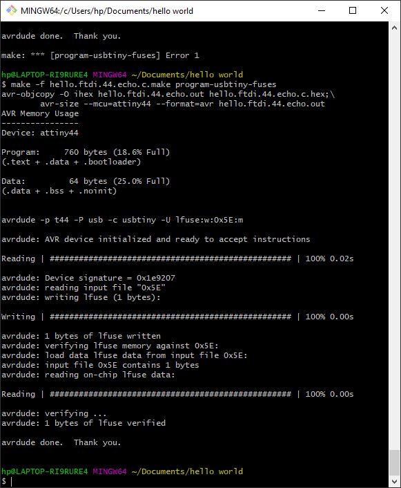
- After that the task is just to add the HEX program on to the board for that you type in the following commands
"make -f 'name of the file.c(hello.ftdi.44.echo.c.make)' program-usbtiny-fuses"
"name of the file.c(hello.ftdi.44.echo.c.make)' program-usbtiny"
If you get the results as seen below, then it is confirmed that the drivers have been loaded to your programmer.
Few things to note
A. The only difficulty in copying the program could be the connections of your board
B. Also you need to solder the jumper on the FAB isp perfectly inorder to avoid the loss of connections. ....