TASK TO DO:
- Learn the software for circuit board design.
- Redraw echo hello-world board.
- Check the design rule,make it and test it.
- Use the test equipment in your lab to observe the operation of a microcontroller circuit board.
- I learn the Eagle software for circuit board design.
Group assignment:
WHAT I HAVE DONE:
This is electronic design week in which we have to learn the circuit design software and redraw the hello board. I am novice for the electronics stuff so this is very new and huge thing for me.
Until I learn PCB milling and programming. So, My local instructor supriya told some basic information about designing software.
Autodesk Eagle :
There are many software for designing the circuit board. So, I downloaded the eagle software and install it on windows.
What is Eagle :-
EAGLE (Easily Applicable Graphical Layout Editor) is a flexible and expandable EDA schematic capture, PCB layout, autorouter and CAM program. EAGLE is popular among hobbyists because of its freeware license and rich availability of component libraries on the web.
There are 2 main steps in designing a PCB in Eagle.
1. Design Schematic - In this section we can add components our PCB and specify the connection between them. we can also add the values of componenets.
2. Design Track-
Here I started designing of my circuit board.
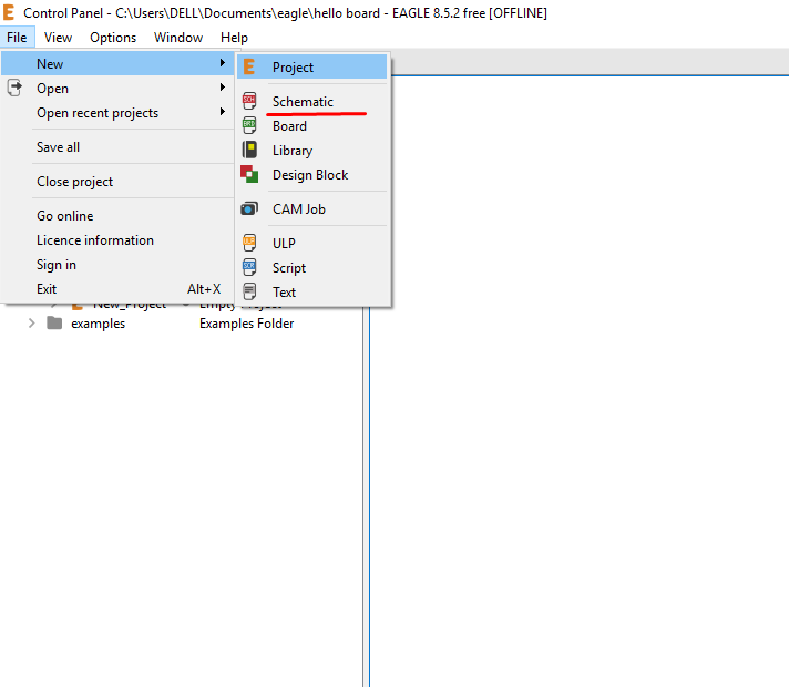
1. Open the eagle then click on the new project and save your project name for Example "hello board". Then select the schematic section.
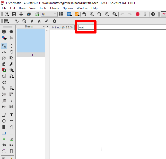
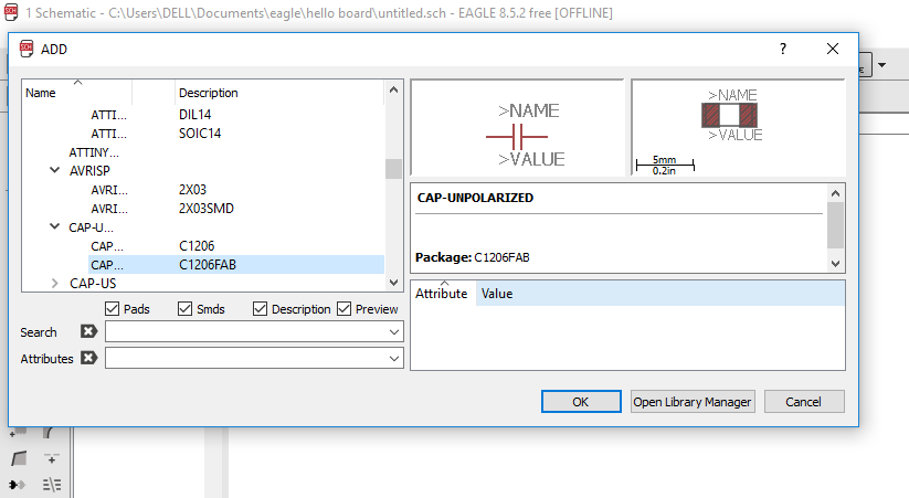
2. Download the fab library (components) and add it to eagle library. For this type "use" in command line of schematic section and search the folder in which you dowanload the fab library and open it.
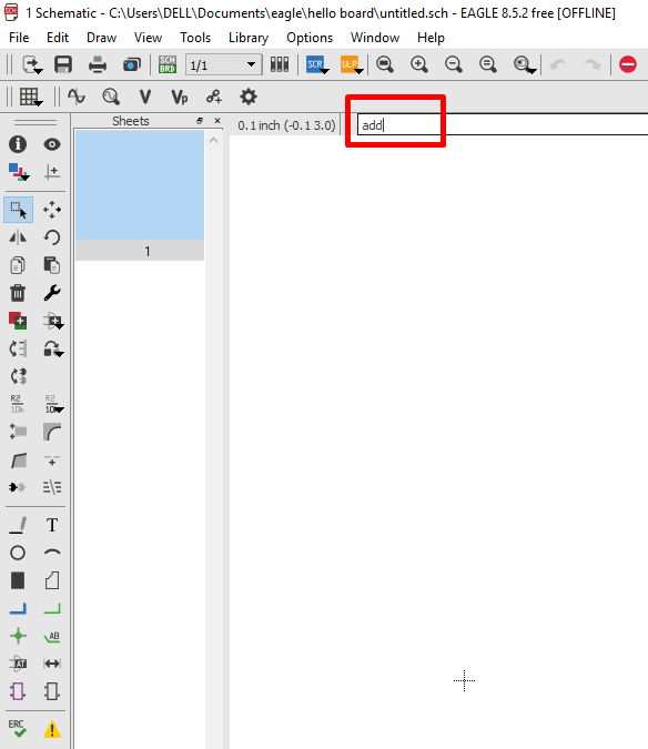
3. After this you have add the component for your PCB. For this type "add" in command line of schematic section and find the fab library.
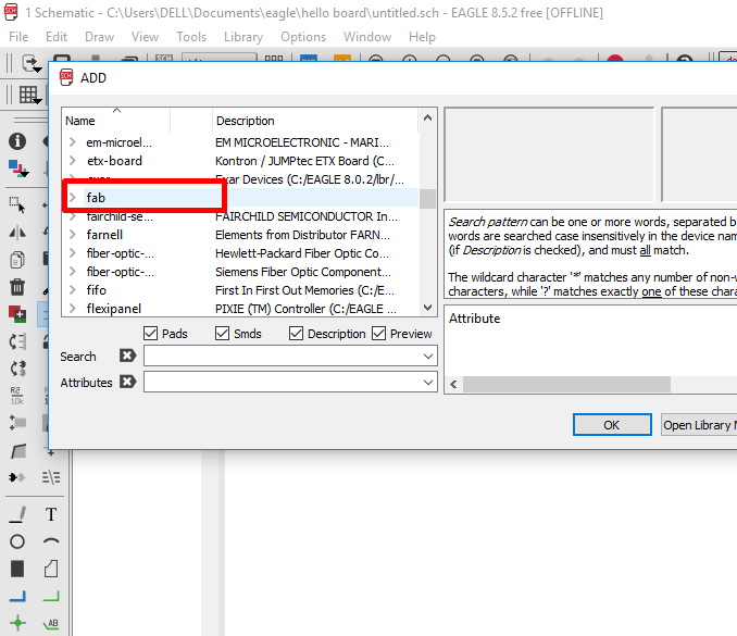
Here You can add all components which you want for PCB. I added resister, capacitor, connectors and Attiny44.
For my hello board I added a LED with limiting resistor and a switch.
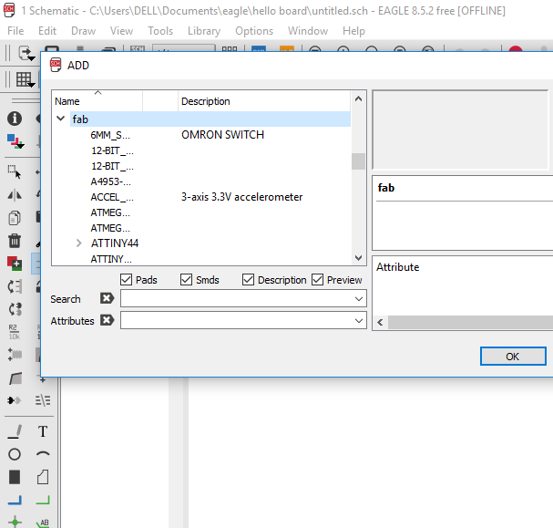
You have to choose all SMD components which are having pads.
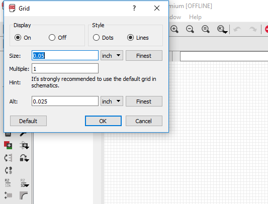
So, all components are in schematic section and its time to connect them. You have make grid visible for better accuracy of connections. Go to view--->grid---> and turn on the display. Make settings (size: 0.05).
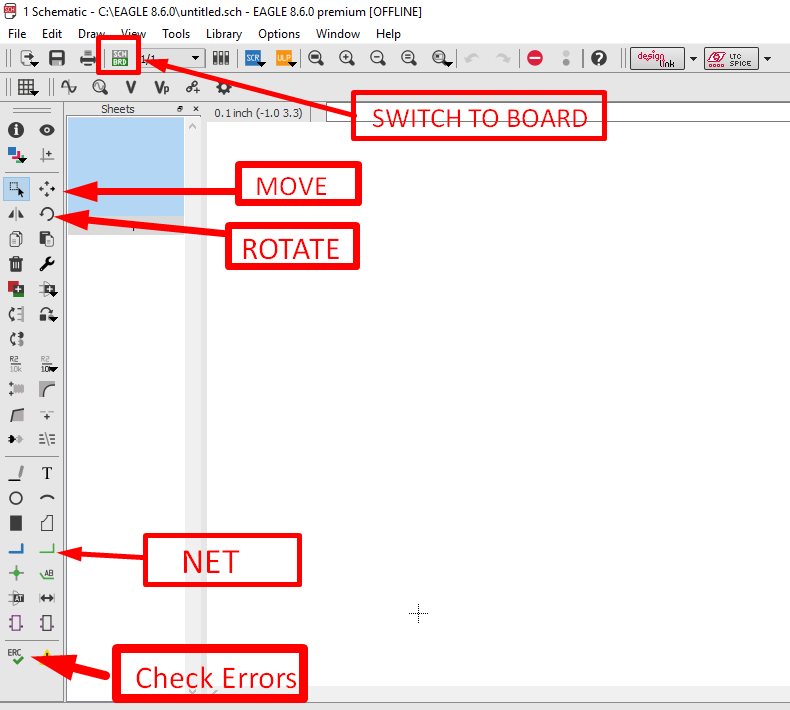
Now I connected all components by using net(green). If two wires connected in a diagram, they are shown with a dot at the intersection.
In schematic section, It doesn't have any problem if the connections are intersect or cross-over. In this section we just specify relation between the components.
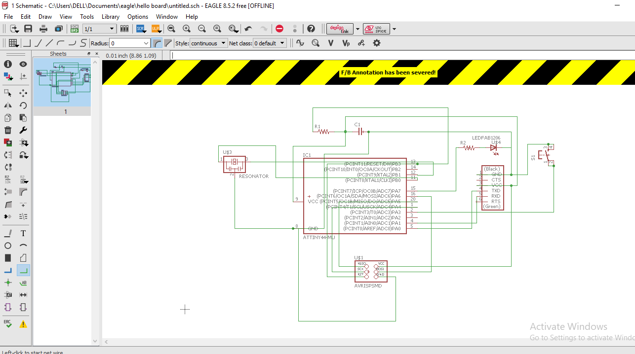
There is also another method to connect the components. We have to just write down the same name for both components which we want to connect.
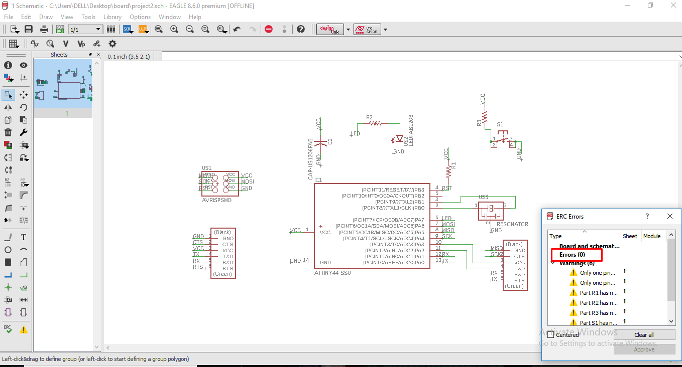
Before switching to board you have to check the errors/warnings. For this just click on the ERC. If errors are found their is option to approve the errors.
But here my schematic doesn't found any error. So I proceed further process.
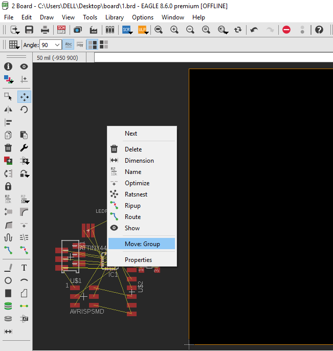
Now we have to chooose switch to board which is on the upper bar. After click on the swith to board one new (black coloured) window appears and all componenets are at the bottom left corner. All componenets are outside the boundary which we have to drag into box. We can drag one by one or in group. For group just select the all componenets and move to file--->group-->then just right click on the selected part and select the "move:group" option.
Now we route the track, for this process we can use the move, mirror, rotate command or options which are available in eagle.
We have align or orient the componenets in such way that no two tracks cross each other. After alignment of componenets I moved towards the routing.
For this, select the route option and just right click on the yellow lines. This traces are in red colour which we can direct as we want.
We have to selelct trace width, for my board I selected 20mil. Also we can choose different traces line as we want which are appears at the upper bar of the window.
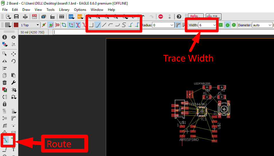
There is also an given option for routing is "AUTOROUTING". It will reduce the time of routing.
Here my board is ready. All traces are made by me.
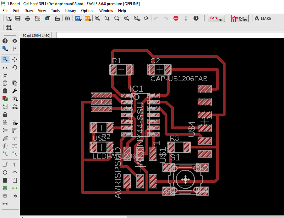
Then I went to my instrutor i.e Supriya for checking board. She suggested me, if possible try to make your project board. Actually in my project, I require four connections. So, I added just one 6 pin connector.
We have to check the dimension and clearance of our circuit and for this click on the DRC.
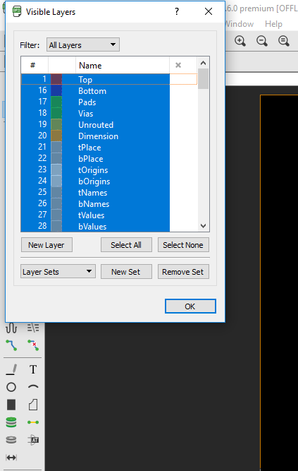
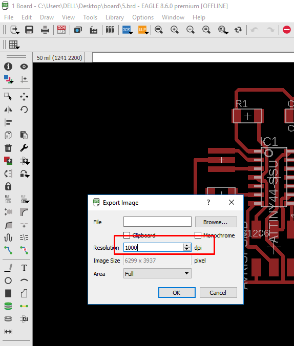
Before going to milling we have to set the border along which the PCB will be cut in modella machine. For this we have to click on layer settings and adjust the dimension layer according to PCB we want. We can also add text in PCB.
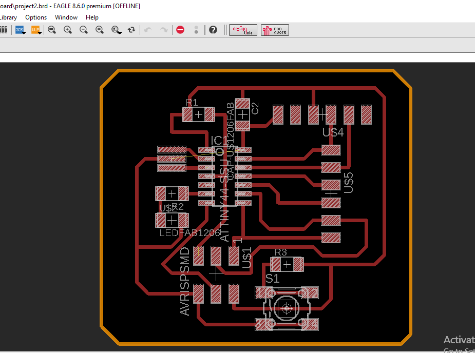
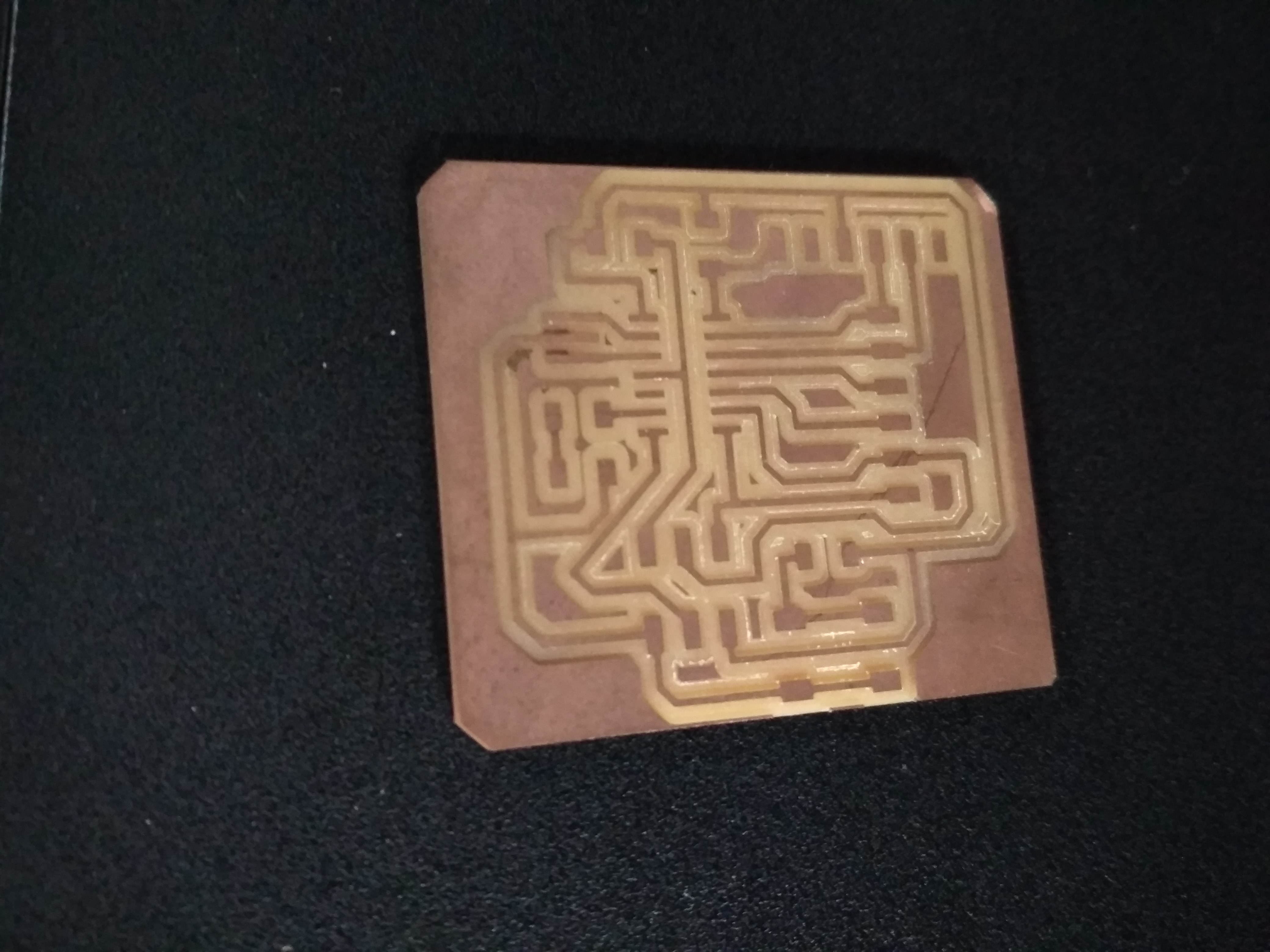
This is my project board after final settings.
Now we have to save seperate .PNG file for Traces and border. For traces in layer setttings select the Top layer and deselect all other layers.
Export this file as .PNG, this is traces file.
Border:-
For Border select Dimensions and deselect other layers and export this file as .png.

Here all design part is done. Now its time to go for milling.
MILLLING -
I already learn milling process in electronics production week. So, I started milling of my board.
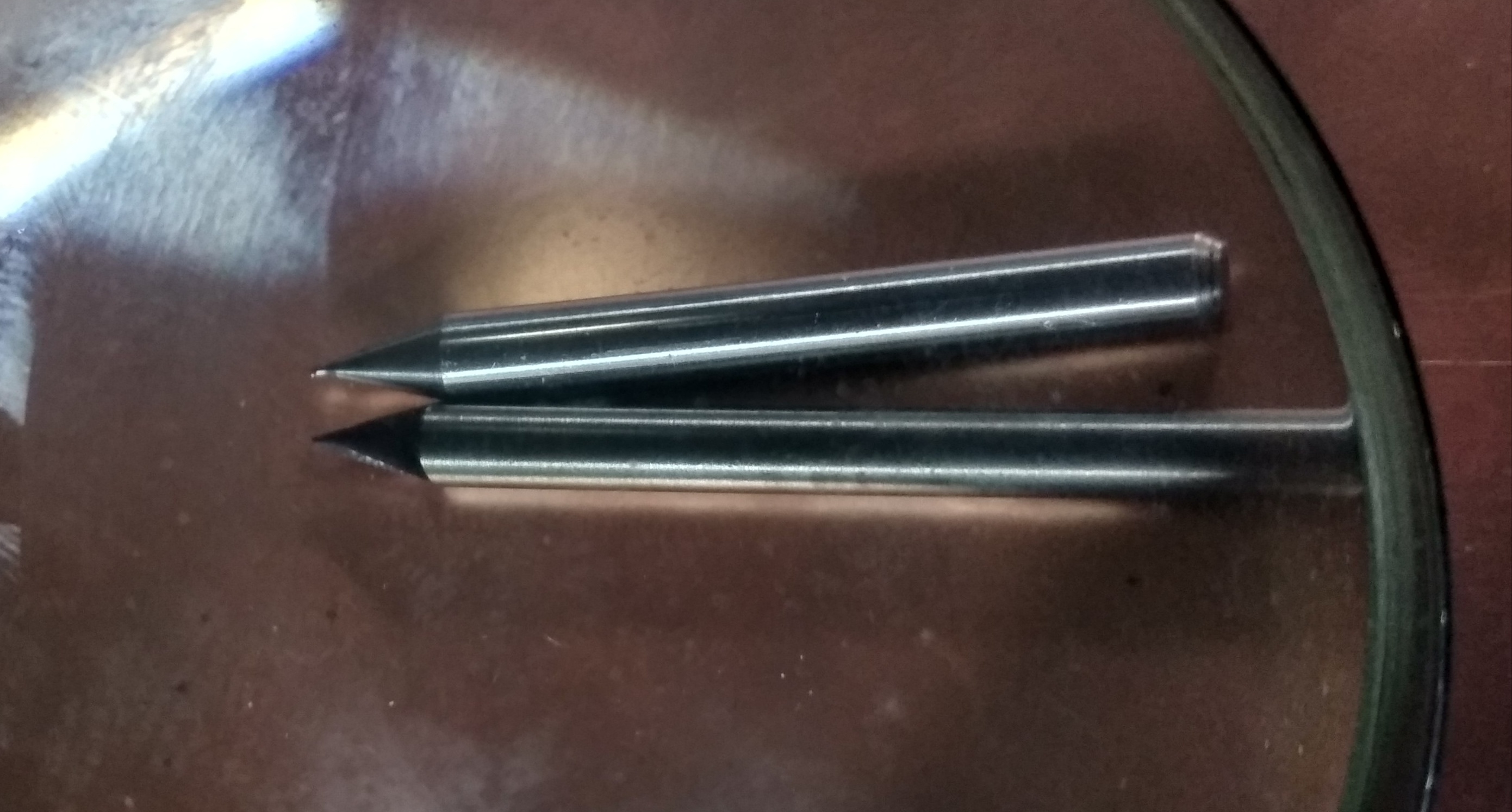
I have .png file which I loaded in fab module and I changed the endmill i.e 1/64 and 4 is offset.
Then I set the gravity and turned towards modella machine.
I started the modella and end mill broken. So, I stopped the milling process. Firstly I thought this happen because of bed level or gravity setting. So, I checked all the settings but everything was correct.
I tried with broken bit but its not good.
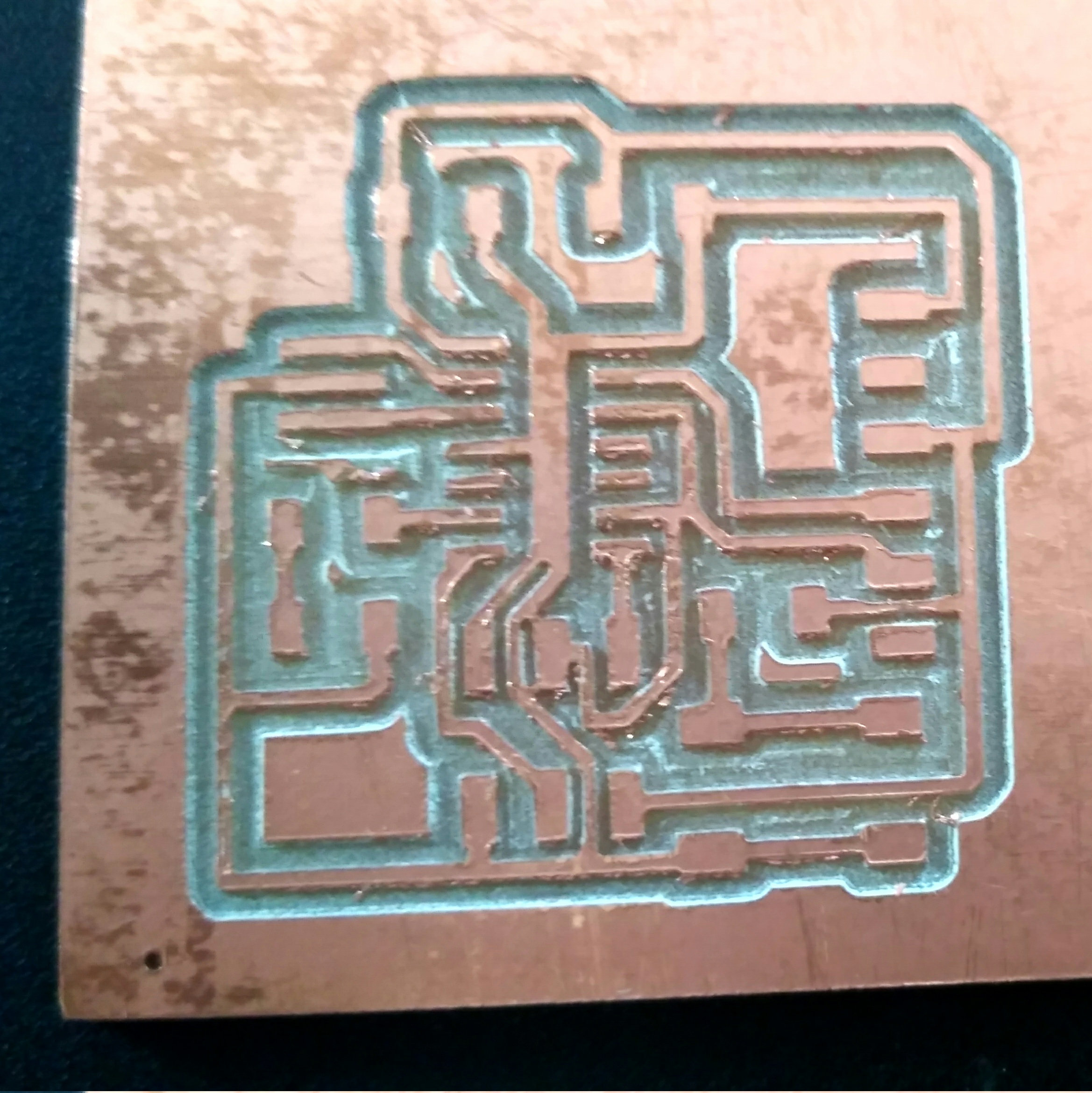
So, I shared this problem with my instructor. Then he tried with new end mill and again the same thing happened. I observed that the end mills are not carbide mills and also they are not good.
Unfortunately this was the last end mill in our lab. HENCE I DID NOT MILL THE BOARD.
So, I decided to mill my board after I get the end mill.
Finally we got the end mills after 2 weeks. Huushhh....!!!
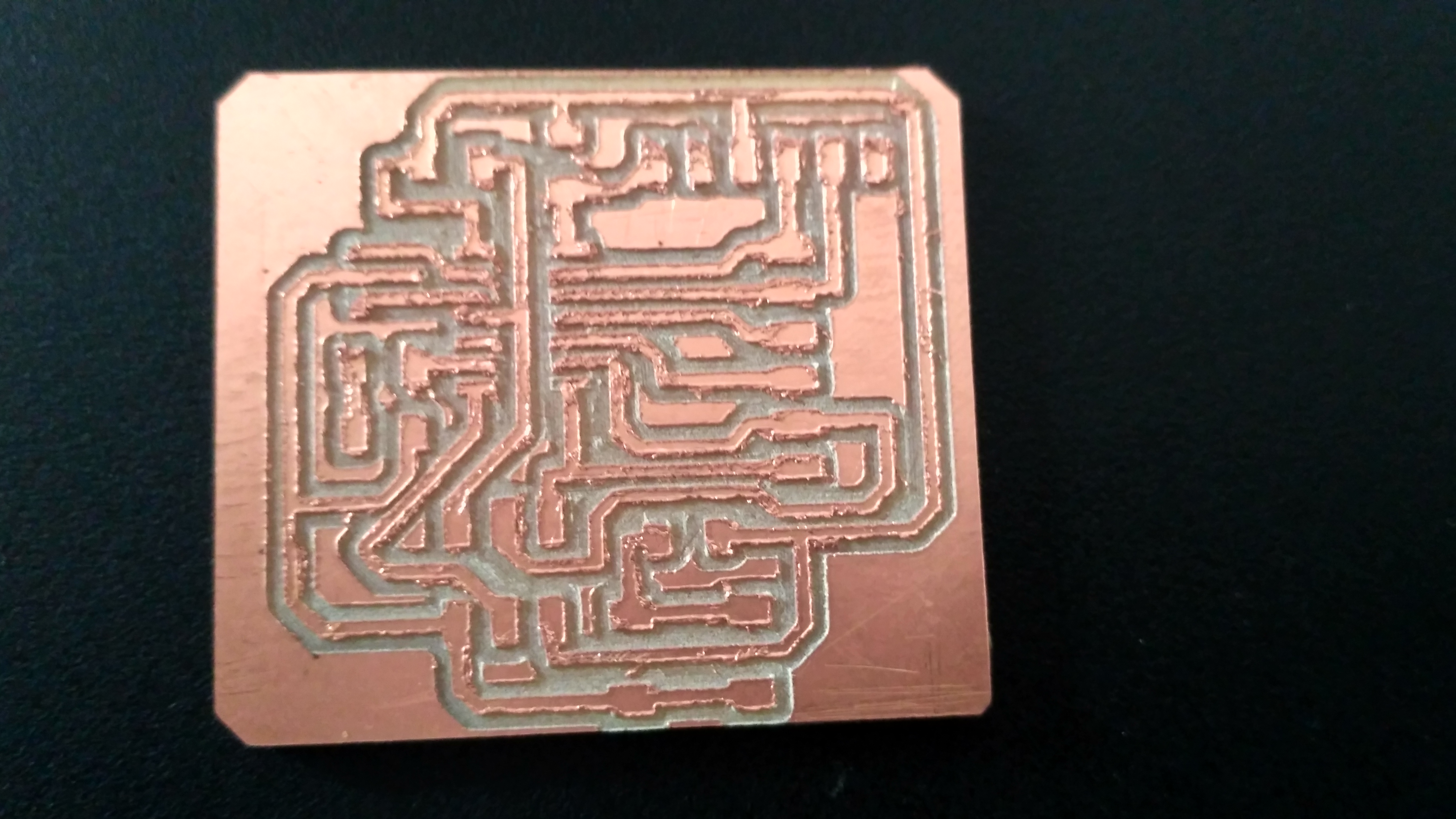
Then I moved towards modella with all settings which explained before. It milled properly. It looks like this.. and it is good.
Soldering-
I collect all the required components i.e
1. A capacitor of 1 micro fahrad
2. A resistor of 499 ohms across the LED (so you don't burn it out)
3. Two resistors 10K ohm each across the Button and Reset respectively
4. A resonator of 20 mHz
5. An LED
6. Pin headers
7. A switch
8. Attiny 44(IC)
and finally I soldered it.
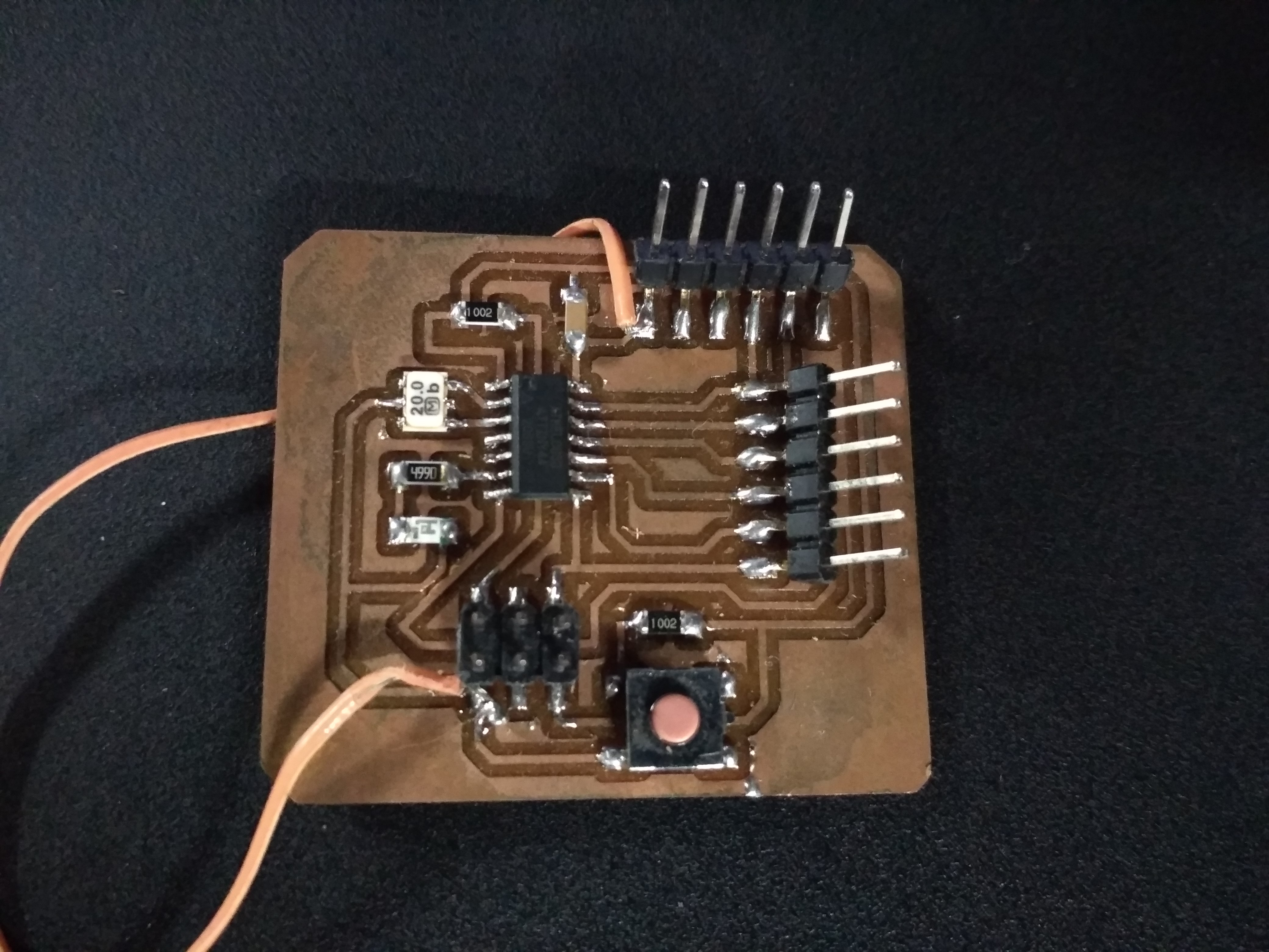
soldering looks well...!!!!
Test the Hello-world board
For testing, We had to load the program in C and python on our board and test it.
Step 1: Firstly check your board is detected or not. Type "lsusb" in the terminal. If it is detected go further.
Step 2: Download the code from here
Step 3: We need to convert our C program to hex file because micro-controller of the board does not understand C. For this, we have to type in the command "make -f 'name of the file.c i.e (hello.ftdi.44.echo.c.make). and then load it.
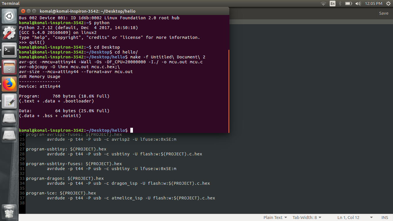
Step 4: After this we have to just add the HEX file on the board. for this type following command in terminal-
"make -f name of the file.c(hello.ftdi.44.echo.c.make)' program-usbtiny"
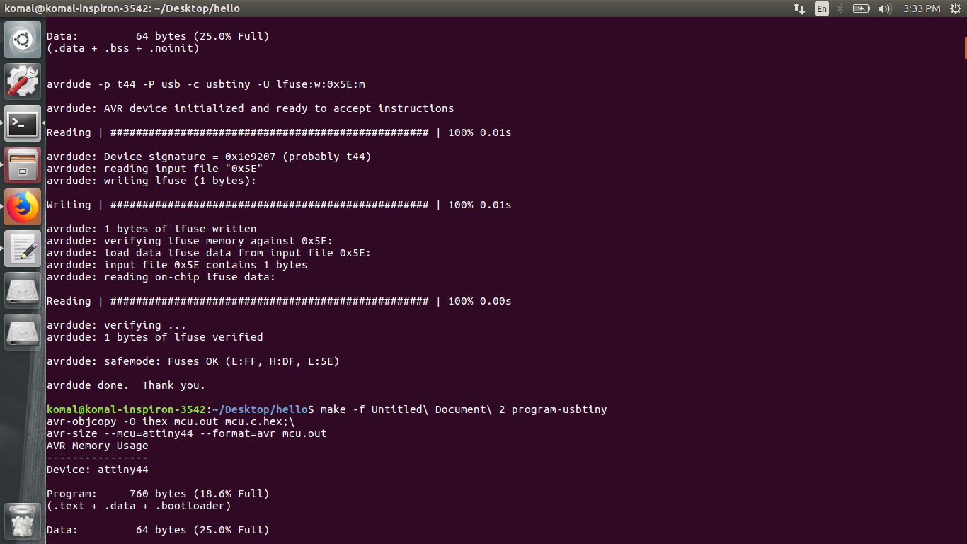
If you get this result then the drivers are uploaded in your board.
Step 5: JUST CHECK IT...!!!
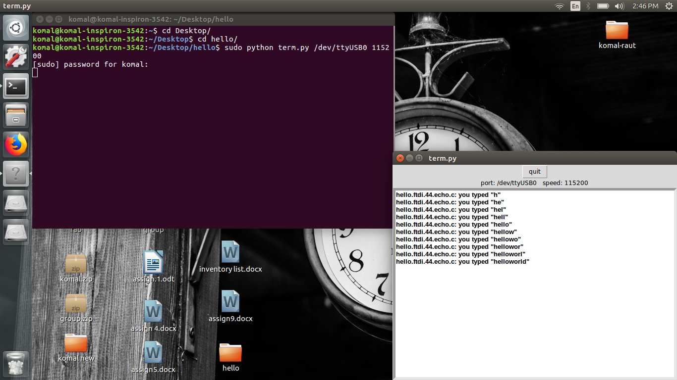
Finally done...!!
You can download original file from here.
Group Assignment:-
Group assignment for this week was to check the operaion of micro-controller board by using various electrical equipments.
The equipments in our lab is as follows:
1. Multimeter-
This device has multiple function as image explained below:
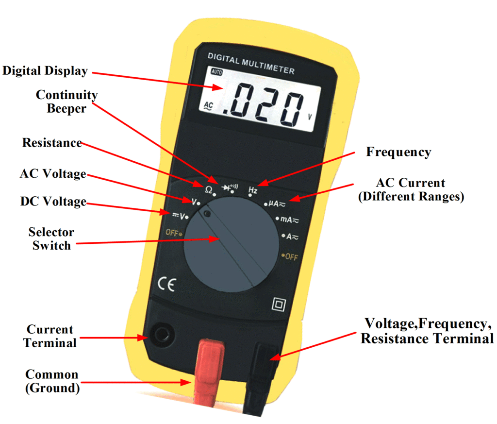
We used it to check the polarities of the LED, resistance and capacitance and the continuity of the circuit board.
2. Oscilloscope-
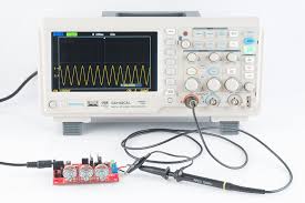
Oscilloscopes are used to observe the change of an electrical signal over time, such that voltage and time describe a shape which is continuously graphed against a calibrated scale. With the help of oscilloscope we tested a hellow world board designed by one of us and had achieved the results as below....
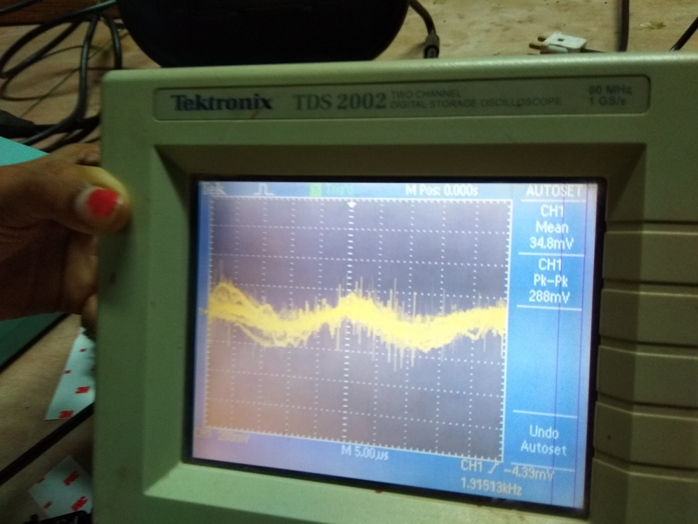
Soldering was not perfect on the position where the oscillator was attached because we can see the wave is in the form of sinusoidal not pulses.
Learning Outcomes-
In this assignment, firstly I learn the Eagle software for circuit designing. I choose Eagle because it has user friendly interface.