Week 7 / Semana 7
use the test equipment in your lab to observe the operation of a microcontroller circuit board
redraw the echo hello-world board,
_________________________________________
Introduction
This week we will design a board by ourselves. We know the process from Electronic Production, now we design it and make it.
group project:
use the test equipment in your lab to observe the operation of a microcontroller circuit board
We
watched a couple of tutorials.
Yo te enseño cómo usar un
multímetro
Aprendiendo a medir
Continuidad con un Multimetro Digital
The
machines we have in the Lab:
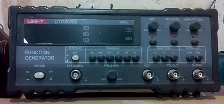
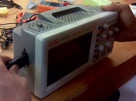
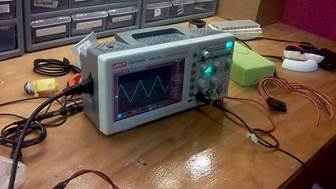
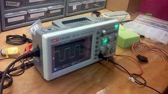
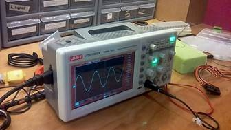
Multimeter 1 / Multimeter 2 / Function Generator / Osciloscope
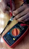
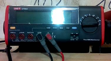
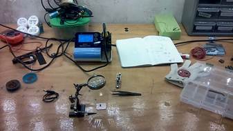
Multimeter 1
1. We use it to test the PCB board we did before
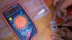
2. We set the Multimeter on 200 ohms
3. We put the red and the black cable each one on the sides of the resistance of 100 ohms
4. Read 100.4 ohms approximately.
5. We repeated the operation but setting the multimeter on 2.000 ohms. The number on the screen was the same.
6. We try again using a resistance we didn´t know the capacity
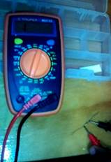
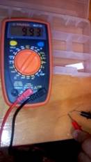
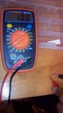
in all the scales appears the same number “1”. So it is a one ohm resistor. If
we don´t know the resistance, we try in the different scale of the multimeter
and check where the value repeats.
7. We tested the oscillator, but unfortunately we couldn’t see any oscillation on the pcb we did. So to check see the machine working we used the function generator. With help we made the machine reproduce a specific Alternating Current (AC)
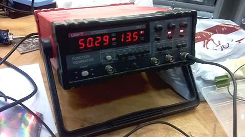
8. The different kind waves
individual project:
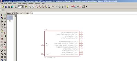
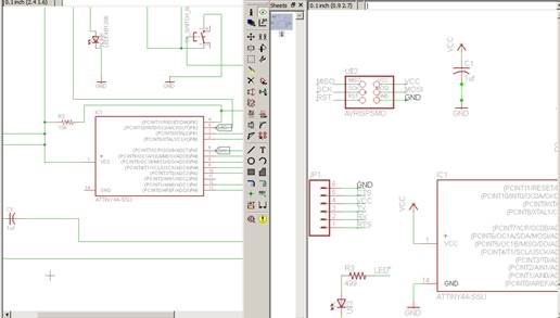
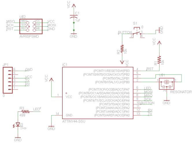
redraw the echo hello-world board,
This is the board I will draw
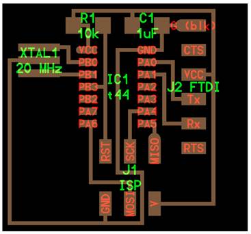
I took the same Assigment of Ilia Feldsthein and Oscar Diaz from last year as reference
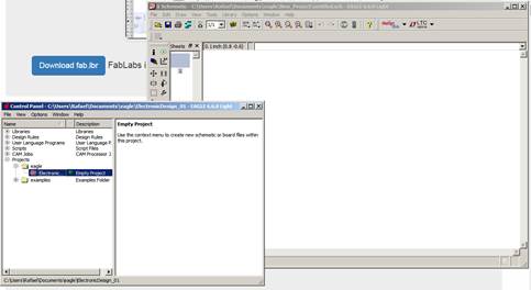
1. Downloaded the Eagle program from Autodesk
2. Downloaded the Fab inventory for Eagle
3. Opened Eagle
4. It doesn´t work on my computer, so I downloaded the version 6. Also downloaded the program on the computer of the Lab
5. Go to FILE menu - NEW - PROJECT. Give it name. ElectronicDesign_01
6. In Eagle control panel, click right mouse button on your new created project and choose NEW – SCHEMATIC
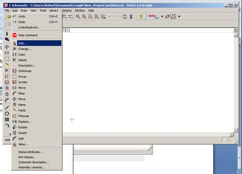
7.
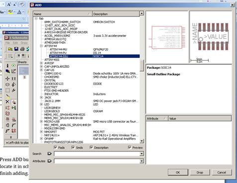
Press ADD
button in side menu - choose component from fab library, press OK and
locate it in schematic window, press ESC and choose the next part or
press CANCEL to finish adding.
Don´t press drop, because the component will disappear from the list
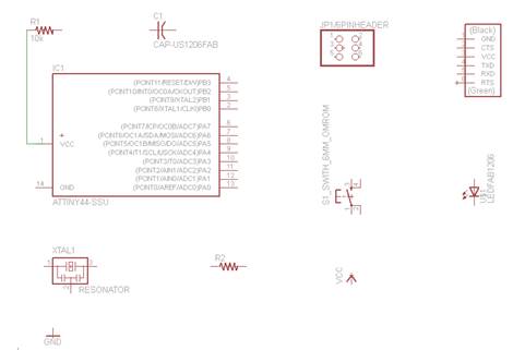
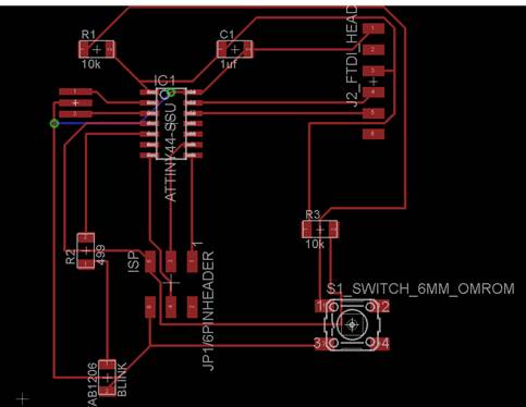
8. I made a list of components.
a. AtTiny44
b. Resistance 10k (x2)
c. Resistor 499 Ohms
d. J1 ISP / 6 pin header programming / PINHD-2X3-SMD (PIN HEADER)
e. J2 FTDI header
f. S1_SWITH_6MM_OMROM
g. LED
h. Capacitor 1uf
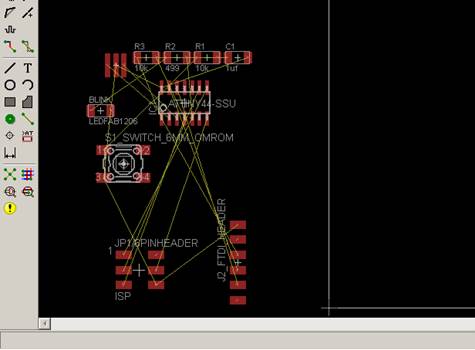
9. I put them all on the schematic
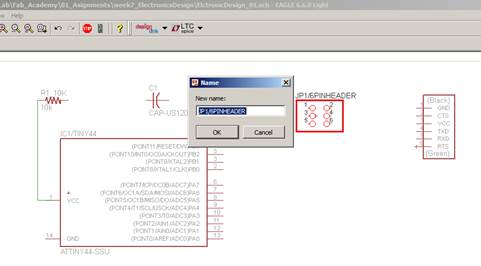
10. Name your components. Write name, the click inside the component and a window will open where you can write the new name
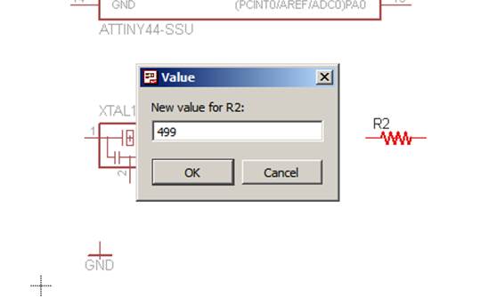
11. Put a Value on the components that have one, like resistors and capacitors
12. I Used the Net command to link all the components
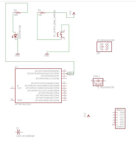
13. I could have linked the components with label also, so I wouldn´t have cables overlapping. But I prefer to connect each component visibly
14. I see I added the button and the led straight while redrawing
15. I think I finished the schematic
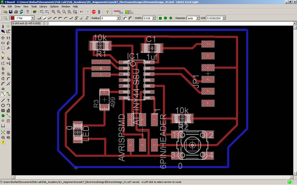
16.
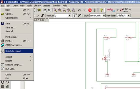
Switch
to board
Menu >> File >> switch to board
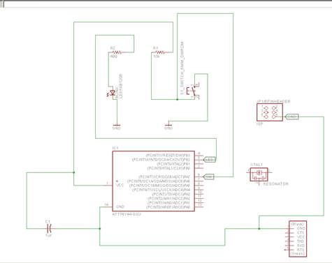
17. Move all the components to right and above the origin mark (cross)
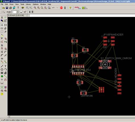
18. I wrote Auto, an window appeared, pressed ok, and the traces appeared in the board view
19. I downloaded a board of the past academy and put the elements in the same way. Put Auto and the traces were much better
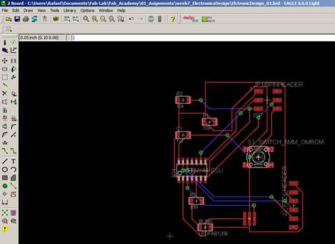
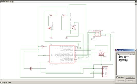
20. I detected I have a wrong connection comparing the schematics
To know what connects with what, click the eye icon (Show) and It will tell you
the turning the type in bold.
21. Had to move and rotate the components till they route on the same side of the pcb
22. I cannot correct that overlapping
24. I checked again that I didn´t have any error. Solved them all.
25.
Now to
the Board again
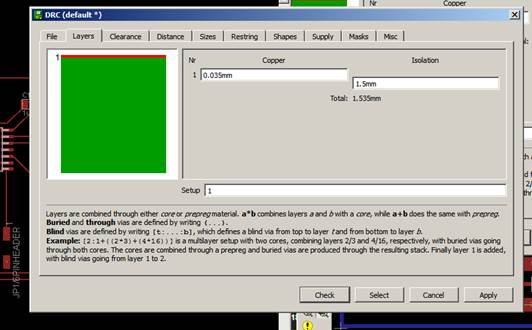
On tools / DRC
Layers/ setup --- 1
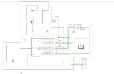
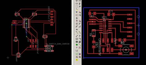
26. Finally. I redraw the whole thing exactly as the reference I used
27.
To the
board once again
28. I think now it is ready, finally!!!
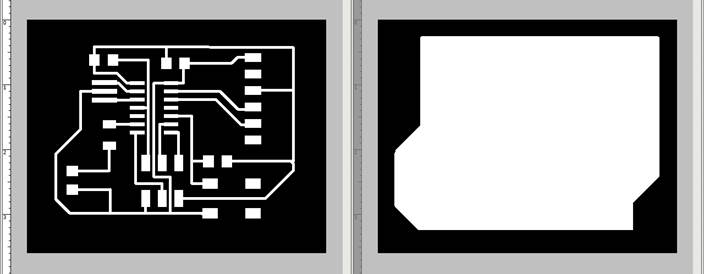
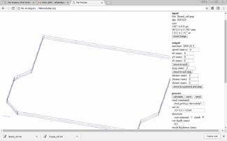
29. In FILE menu go to EXPORT and choose IMAGE. Give it name and location, set resolution to 600 dpi MONOCHROME. DO it separately for the top (traces and pads) and the bottom (outline) layers. You should get this way two PNG files, one for traces and pads milling and second for outline cut out milling.
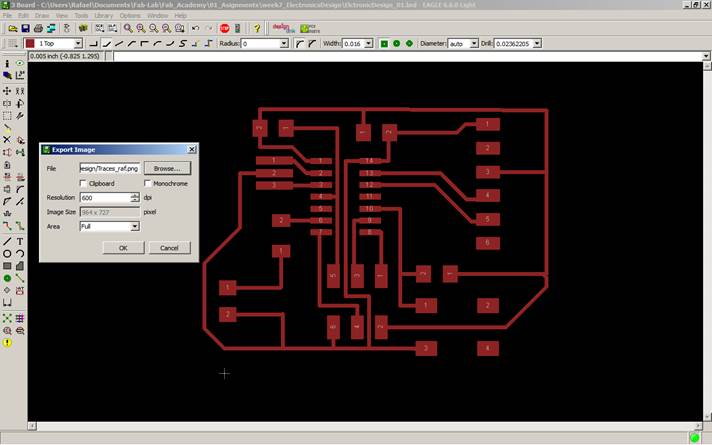
30. Opened the files in Photoshop
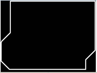
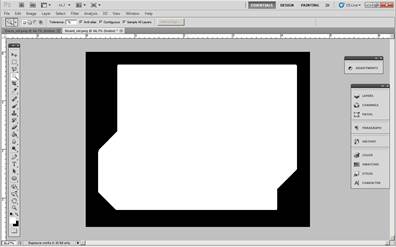
31. The board or outline needed an extra frame because the line was too close to the boundaries of the image. And also the inside in white. I just select the inside with the magic wand with continuous option checked
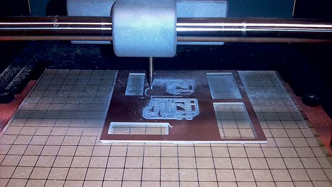
32. Two unfortunately things happened
a. The end mill broke two times
b. I changed the canvas of the outline making it bigger to get the shape, but didn´t do the same on the trace png, so apparently the origin was not the same and the Roland cut the outline displaced
33. I made the two png´s the same size
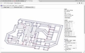
34. Made the .rtml again with fabmodules. I still have to learn how to use Mods
35. Tomorrow I will fabricate a new pcb
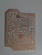
36. And I did it
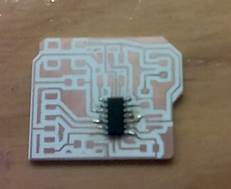
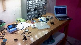
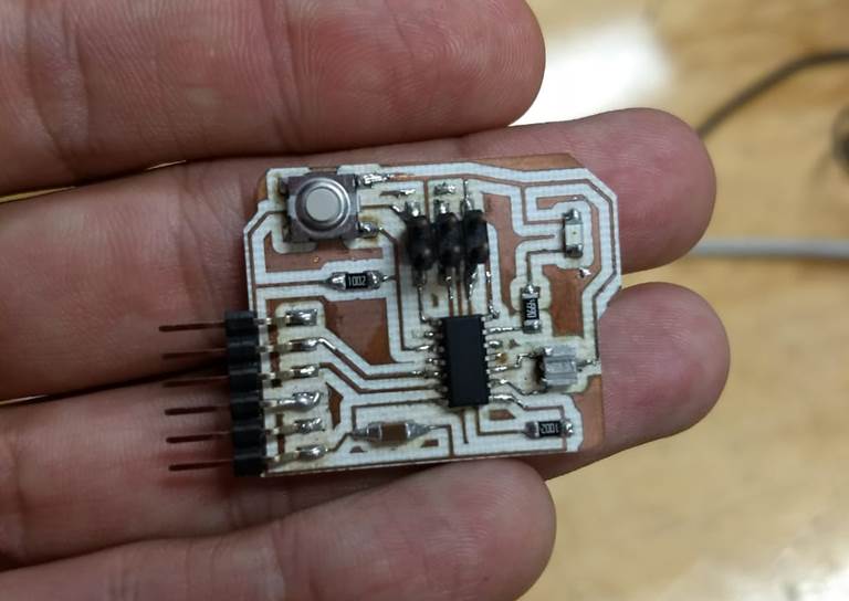
37. Me soldering
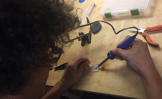
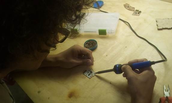
38. The result
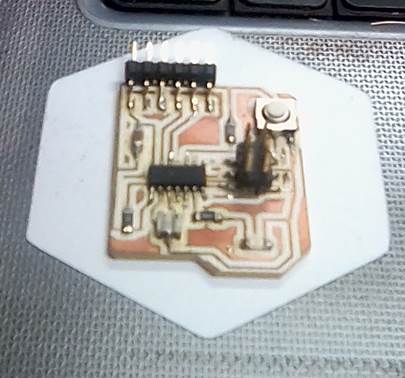
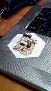
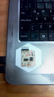
Hero Shot
Conclusions
· Each board has passive and active components. The passive are the components that must exist in the board for the minimum functionality, like the microprocessor, a couple of resistances and the crystal. The active are the components that adapt the board to specific needs, for instance in this case the LED and the button will be actives
· The eagle helps on the auto arrangement of the components and its traces, but still you have to edit it to avoid overlapping of traces.
· After soldering checking that the traces are not making contact with each other will save time.
Download files / Descargar archivos