Week 7
Electronics Design
Group assignment
- Use the test equipment in your lab to observe the operation of a microcontroller circuit board
Individual assignment
- Redraw the echo hello-world board, add (at least) a button and LED (with current-limiting resistor), check the design rules, make it, test it.
Learning outcomes:
- Select and use software for circuit board design
- Demonstrate workflows used in circuit board design
Have you:
- Shown your process using words/images/screenshots
- Explained problems and how you fixed them, including how you worked with design rules for milling (DRC in EagleCad and KiCad)
- Included original design files (Eagle, KiCad, Inkscape, .cad - whatever)
Week workflow
weekly assignment → introduction to eagle → Edit Schematic/Boad → Mill the board→ solder components → debug → edit and publish website
Tools used
- Solder Station
- TaoBao CNC
- test equipment: digital voltmeter, oscilloscope, regulated power supply
Software Used
- Eagle
- Fab Modules
- Gimp
Design files of hello board
- zip of eagle source files
- internal jpeg to cnc
- external jpeg to cnc
- Using the test equipment in our lab
-
I started by watching a sparkfun's youtube video on an oscilloscope
I learned: - that an oscilloscope measures voltage over time: getting amplitude, frequency, transient signals;
- The important buttons...
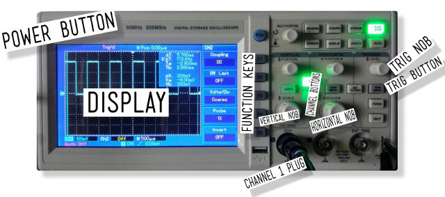
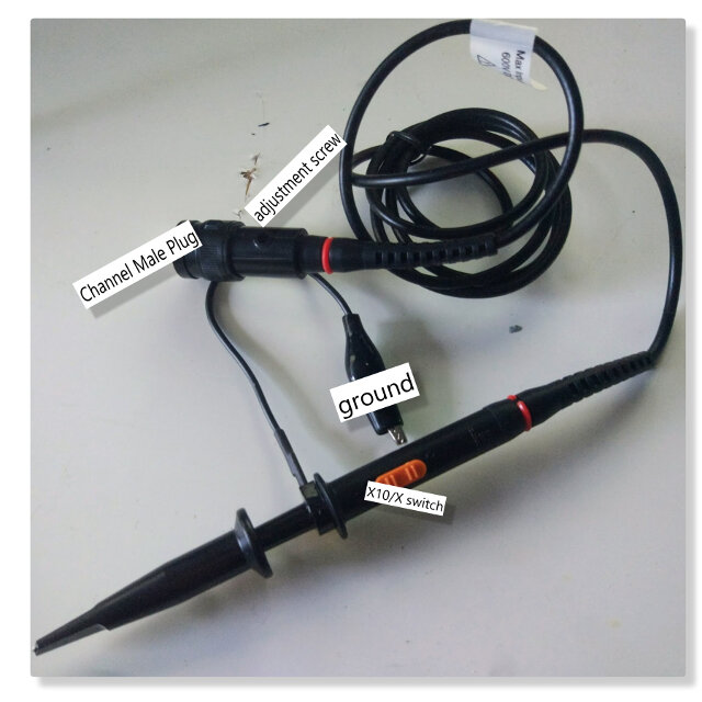
- Calibrating the probe/Adjusting compensation capacitor
- on the probe select to X10;
- connect the probe to channel one plug;
- connect the probe to the 1kHz 5V square wave generator
- turn on oscilloscope
- make sure only channel one is on, click on CH2 button until its off and the other way around on CH1 button;
- select DC coupling with the F1 key;
- press button F4 to select 10X on probe mode;
- press trig/menu button and select type as "edge" and source CH1
- Select slope as "Rise"
- Adjust the Vertical and horizontal knobs until you see the wave
- if wave is moving adjust trig knob until it stops
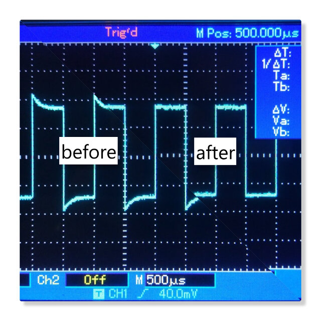
- to calibrate the probe adjust the screw on the base of the probe until the wave is square.
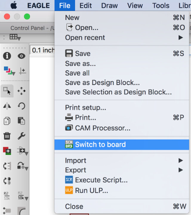
- Eagle introduction:
- I started by watching the video tutorials below I had a look through the eagle tutorial for the week 6. Following it I downloaded and installed the Fab library for eagle.
-
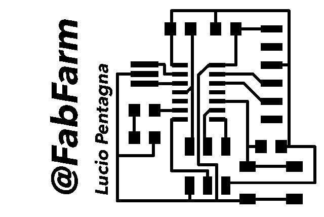
Reverse engineering Neil's Board
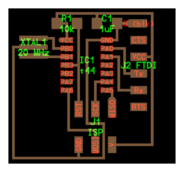
- I started by having a look at the Electronics Design - Eagle tutorial With the above schematics in hand I started redrawing it at Eagle
- Schematics Step by Step:
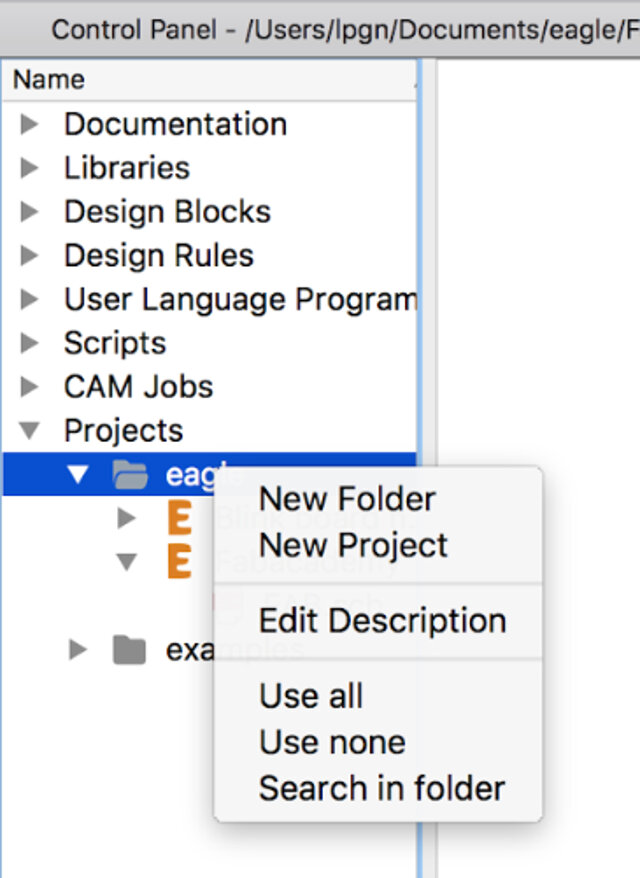
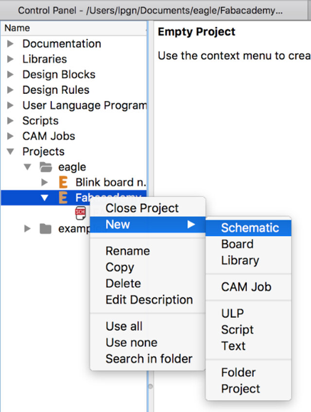
- under projects → right-click on eagle → click on new project → name project
- right-click on project name → new→ Schematic
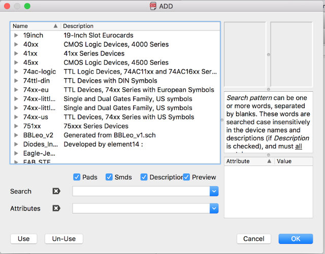
- type "add" → search for each part
- place part with let click → repeat procedure until all the same part is added → press ESC to add next part → search for next part or press ESC to go back to schematics
- Type "rotate" and left click on part origin to turn part around to desired position
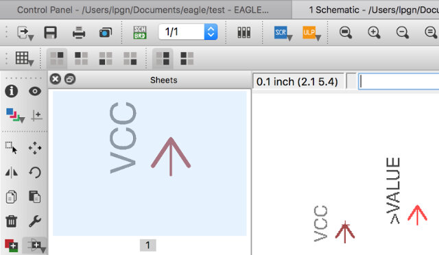
- Type "net" to connect part to each other;
- type "name" and left click on top of part to name part;
- type "label" and left click on wire to connect one to the other without having to net;
- type value and left click on part origin to designate part "value";
- type "move" to position the part as needed
- save the file
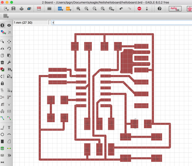
- Drawing the Board
- Left click on file → type "board" → accept warning and left click yes to create start designing the PCB from previously created schematics
- all components will be displayed to the left of the board → Drag them one by one with command "move"+left click drag to position inside the board
- type "rotate" to turn the components the same way as in the schematics
- after all is positioned → resize board size dragging the sides of the original board with the command "move"
- type "polygon" and select top layer and draw a square around the board limits in order to creat he top layer of the PCB
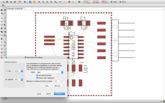
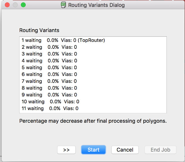
- type "ratsnest" → start autorouter type "auto", this command is very convenient as it gives initial idea on how you can route the board, but it doesn't replace manual routing
- select start
- adjust traces if needed with command "ripup" to remove positioned paths
- place new paths with command "route" and "move" to better position
- type command "info"+left click in order to fine tune position of paths as well as thickness
- Adding the LED and Button
- In order to add the LED and the Button I went back to the Schematics.
- In the schematics type "add" to add two resistors, one LED and the button
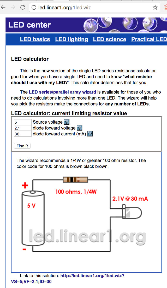
- The fist resistor works to limit the current that goes to the LED. It should be placed in the positive side of it. In other to dimension the LED I checked first the LED data sheet. There I looked for, Dc forward current, in this case 30 and forward voltage, in this case 2.1.
- with those two values plus my input voltage "5" in hand I input the values to the website LED center in other to calculate the correct resistor, in this case 100Ohms
- as for the switch I used a 10K resistor as a pull-up resistor
- like before I used the commands move rotate and label name copy to position all components on its place
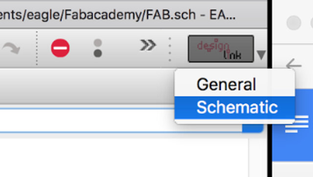
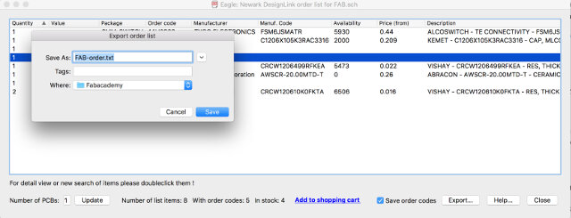
- Make BOM (Bill of Materials)
- Left click on design link → left click on Schematic
- wait for program to display part → type new search string in case desired part does not appear → left click manual search → choose desired part → left click select
- repeat previous process until all parts are found
- left click export and save BOM File
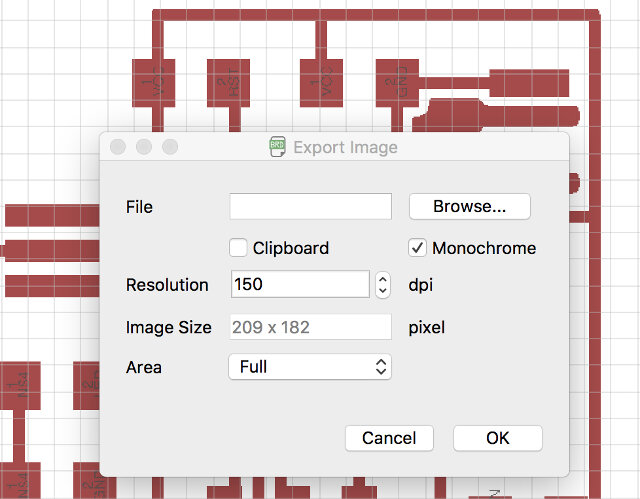
- Exporting the image for fabmodules
- Go to Options, Set, Misc and deselect Display Pad names, signal and via lengths. This will prevent undesired text from appearing on the exported image.
- On layers toolbar select only the top layer
- next type "export"→ select image nd monocromatic→and in resolution type 500
- save to desired location
- the result is a black and white image
- Edit in gimp
- With the exported eagle file in hand open in gimp.
- in gimp I decided to add some wording, this was easy by selecting the text tool, then font size and rotating the wording to an ideal location.
- I also removed unnecessary black areas with the bucket tool
- to create the outline I selected the area I wanted to keep and covered it with the bucket tool
- in the end you should have two images, one for the PCB and one for the outline
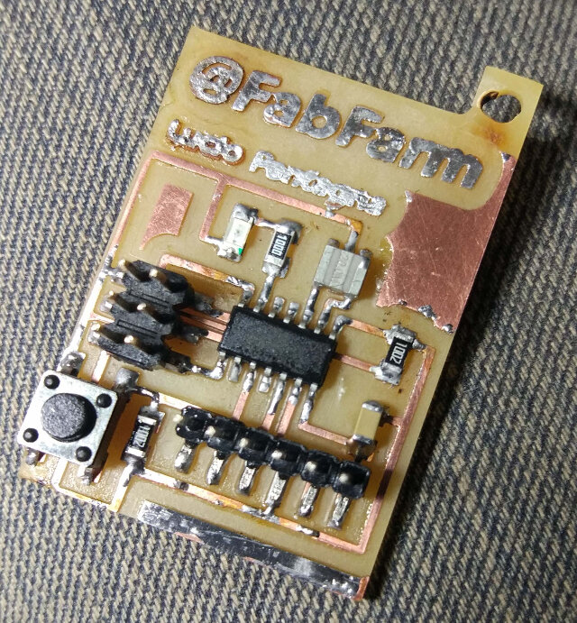
- Fab modules and Milling
- Soldering/Populating the PCB and Debuging
- Conclusion
To position the components on the PCB use commands as done on the schematics:
You can watch how I did it here, pump up the volume for some Cash!
in case it doesn't play watch it on youtube!

After some editing here it is:
| qty | Location | Digikey or Mouser Part number | Manufacture Part # | Description |
|---|---|---|---|---|
| 1 | U1 | ATTINY45V-10SU-ND | ATTINY45V-10SUR | IC MCU 8BIT 4KB FLASH 8SOIC |
| 2 | R1 | 311-10.0KFRCT-ND | RC1206FR-0710KL | RES SMD 10K OHM 1% 1/4W 1206 |
| 1 | R2 | 311-100FRCT-ND | RC1206FR-07100RL | RES SMD 100 OHM 1% 1/4W 1206 |
| 1 | D3 | 160-1169-1-ND | LTST-C150GKT | LED GREEN CLEAR 1206 SMD |
| 1 | C1 | 445-1423-1-ND | C3216X7R1H105K160AB | CAP CER 1UF 50V X7R 1206 |
| 1 | FTDI | 6 pin header | ||
| 1 | RESONATOR | XC1109CT-ND | ECS-CR2-20.00-B-TR | CER RES 20.0000MHZ 15PF SMD |
| 1 | 450-2058-1-ND | FSM6JSMATR | SWITCH TACTILE SPST-NO 0.05A 24V | |
| 1 | ISP | 649-95278-101A06LF | 71600-006LF | Headers & Wire Housings 2X3P UNSHRD HDR 30 micro inch gold |

The process in Fab modules and Milling is already outlined by the week 4 assignment so I will only keep here an image of the result
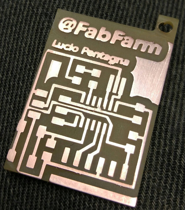
The result
As before the populating and debugging is already outlined by the week 5 assignment so I will only keep here an image of the result
I really enjoyed learning this new tool. I have used eagle before to view pcb's but never actually designed one. I feel it opens my mind to a lot of new things to come!