7. Electronics design
-
The goal for this week was to Design Electronics, print the pcb board and solder components to make it and test with a button and LED.
-
We were given the task to copy Neil’s Hello echo board using tools like Eagle or KiCad.
-
Not Only the Designing we were given the task to know the all ERC and DRC i.e Design Rules and electrical chek rules for the design and to route it and mill it.
-
My responsibility was to start with schematic on KICAD or Eagle, associate components with the fab library and mods, also create the connection traces in order to calculate the png file for the pcb interior and outline on fab academy modules website.
Useful links
- Libraries For Kicad & Eagle
- KiCad
- Autodesl Eagle
- KiCad Auto Rerouting
- KiCad Auto Rerouting Video
- Jeremy Blum Eagle Tutorial
- PCB.py
Getting Started with PCB Design
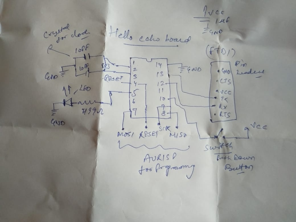
Before i started with any of the software our instructor mentioned to first design the schematic on a piece of paper. Neil has shared his hello board already that had lot of information available for design and we were just suppose to add the button and LED to hello board.
I considered some basic design rules to make this schematic on paper like adding some pull down / pull up resistors. Understanding the pin layout of Attiny 44 , FTDI and AVRISP connections.
Here is the schematic on paper.
Getting Started PCB.py
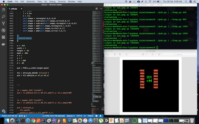
Objective of this week was to try as many software so i started with something that sounded familiar to me. So i started by downloading the PCB.py. One of the prerequistes for the program is that you have python and dependent libraries installed and you have to make the file executable. Mac already comes with python installed but i installed Anaconda Python as it comes bundled with all the dependencies required for running PCB.py. I followed the instructions available on github and simply executed the command by commenting few sections of the code. I opened three windows one for my code, one for image and one for terminal on how Neil showed that in his lecture.
make these executable:
   chmod +x pcb.py
   chmod +x frep.py
execute:
   pcb.py | frep.py
view:
   out.png
optional arguments:
   pcb.py | frep.py dpi
   pcb.py | frep.py dpi filename
dependencies:
   Python
   NumPy
   Python Imaging Library
How an IC chip is drawn
Basically for each component Neil has written a Python class that draw that component like as we are using ATtiny44 IC below class is written that draws the pads and shape for ATtiny44
class ATtiny44_SOICN(part):
   def __init__(self,value=''):
      self.value = value
      self.pad = [point(0,0,0)]
      self.labels = []
      #
      # pin 1: VCC
      #
      self.shape = translate(pad_SOICN,-.12,.15,0)
      self.shape = add(self.shape,cylinder(-.155,.15,0,0,.015))
      self.pad.append(point(-.12,.15,0))
      self.labels.append(self.text(self.pad[-1].x,self.pad[-1].y,self.pad[-1].z,'VCC'))
      #
      # pin 2: PB0/XTAL1/PCINT8
      #
      self.shape = add(self.shape,translate(pad_SOICN,-.12,.1,0))
      self.pad.append(point(-.12,.1,0))
      self.labels.append(self.text(self.pad[-1].x,self.pad[-1].y,self.pad[-1].z,'PB0'))
      #
      # pin 3: PB1/XTAL2/PCINT9
      #
      self.shape = add(self.shape,translate(pad_SOICN,-.12,.050,0))
      self.pad.append(point(-.12,.05,0))
      self.labels.append(self.text(self.pad[-1].x,self.pad[-1].y,self.pad[-1].z,'PB1'))
      #
      # pin 4: PB3/dW/-RESET/PCINT11
      #
      self.shape = add(self.shape,translate(pad_SOICN,-.12,0,0))
      self.pad.append(point(-.12,0,0))
      self.labels.append(self.text(self.pad[-1].x,self.pad[-1].y,self.pad[-1].z,'PB3'))
      #
      # pin 5: PB2/CKOUT/OC0A/INT0/PCINT10
      #
      self.shape = add(self.shape,translate(pad_SOICN,-.12,-.05,0))
      self.pad.append(point(-.12,-.05,0))
      self.labels.append(self.text(self.pad[-1].x,self.pad[-1].y,self.pad[-1].z,'PB2'))
      #
      # pin 6: PA7/ADC7/OC0B/ICP/PCINT7
      #
      self.shape = add(self.shape,translate(pad_SOICN,-.12,-.1,0))
      self.pad.append(point(-.12,-.1,0))
      self.labels.append(self.text(self.pad[-1].x,self.pad[-1].y,self.pad[-1].z,'PA7'))
      #
      # pin 7: PA6/ADC6/MOSI/SDA/OC1A/PCINT6
      #
      self.shape = add(self.shape,translate(pad_SOICN,-.12,-.15,0))
      self.pad.append(point(-.12,-.15,0))
      self.labels.append(self.text(self.pad[-1].x,self.pad[-1].y,self.pad[-1].z,'PA6'))
      #
      # pin 8: PA5/ADC5/DO/MISO/OC1B/PCINT5
      #
      self.shape = add(self.shape,translate(pad_SOICN,.12,-.15,0))
      self.pad.append(point(.12,-.15,0))
      self.labels.append(self.text(self.pad[-1].x,self.pad[-1].y,self.pad[-1].z,'PA5'))
      #
      # pin 9: PA4/ADC4/USCK/SCL/T1/PCINT4
      #
      self.shape = add(self.shape,translate(pad_SOICN,.12,-.1,0))
      self.pad.append(point(.12,-.1,0))
      self.labels.append(self.text(self.pad[-1].x,self.pad[-1].y,self.pad[-1].z,'PA4'))
      #
      # pin 10: PA3/ADC3/T0/PCINT3
      #
      self.shape = add(self.shape,translate(pad_SOICN,.12,-.05,0))
      self.pad.append(point(.12,-.05,0))
      self.labels.append(self.text(self.pad[-1].x,self.pad[-1].y,self.pad[-1].z,'PA3'))
      #
      # pin 11: PA2/ADC2/AIN1/PCINT2
      #
      self.shape = add(self.shape,translate(pad_SOICN,.12,0,0))
      self.pad.append(point(.12,0,0))
      self.labels.append(self.text(self.pad[-1].x,self.pad[-1].y,self.pad[-1].z,'PA2'))
      #
      # pin 12: PA1/ADC1/AIN0/PCINT1
      #
      self.shape = add(self.shape,translate(pad_SOICN,.12,.050,0))
      self.pad.append(point(.12,.05,0))
      self.labels.append(self.text(self.pad[-1].x,self.pad[-1].y,self.pad[-1].z,'PA1'))
      #
      # pin 13: PA0/ADC0/AREF/PCINT0
      #
      self.shape = add(self.shape,translate(pad_SOICN,.12,.1,0))
      self.pad.append(point(.12,.1,0))
      self.labels.append(self.text(self.pad[-1].x,self.pad[-1].y,self.pad[-1].z,'PA0'))
      #
      # pin 14: GND
      #
      self.shape = add(self.shape,translate(pad_SOICN,.12,.15,0))
      self.pad.append(point(.12,.15,0))
      self.labels.append(self.text(self.pad[-1].x,self.pad[-1].y,self.pad[-1].z,'GND'))
To draw this you simply need to create an Object and add it to PCB object
pcb = PCB(x,y,width,height,mask)
IC1 = ATtiny44_SOICN('IC1\nt44')
pcb = IC1.add(pcb,x+.47,y+.59,z)
And this is how it would look, super easy
Putting up AVRISP on PCB
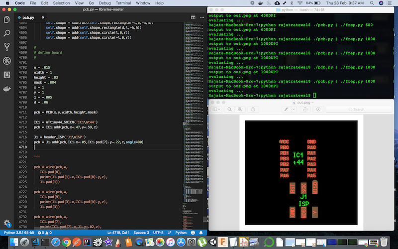
How wire is drawn from one component to another

Overall Learning Outcomes from PCb.py
- We can draw PCB using simple python code
- No option for autorouting, we have to do it in code manually
- No option for design rules check available
- Need understanding on how component look like to enhance this code
- It is a good tool if you are good in electronics design and know what are you doing
- No option to use pre built libraries like you can use in KiCad and Eagle
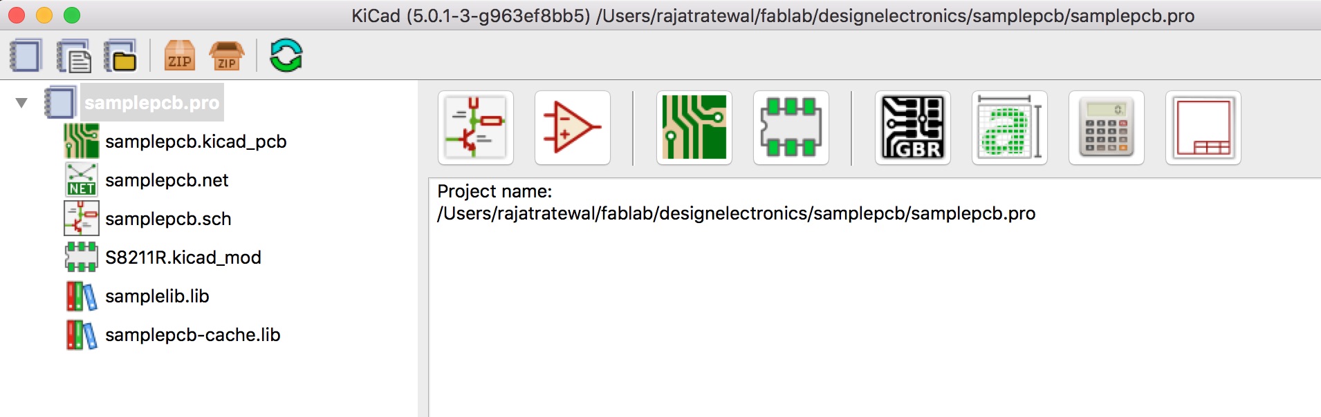
Getting Started KiCad
As this was new tool so i followed following links shared in fablab KiCad Resources
In this i found the very much needed video tutorial to create schematic, draw footprints and route the board. So i simply watched the videos and tried to replicate the same on my machine.
KiCad is an open source program and its been made as part of various other programs, which are accessible via the KiCad menu. So i learnt about following things by following the tutorial
- Getting familar with KiCad interface
- Cheat sheet for KiCad shortcuts, this is extremly useful while drawing schematic
- I was able to draw a schematic by following the tutorial this covers importing library, creating a footprint
With getting some basics on interface i decided to start with week assigment that was to mill, solder and program a hello board. So i followed the assignment week page from our lab manager Darshan on how he has designed the hello board in KiCad
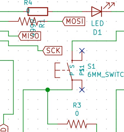
Keeping in reference the Neil’s board, we had to just add a Resistor, LED and a Button.
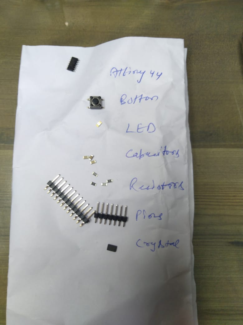
So first step was to identify all the components. All the respective Libraries For Kicad & Eagle for component with footprints was already shared for us to use in this week.
- ATTINY 44 its a microcontroller
- FTDI This is a USB to TTL serial cable, with a FTDI FT232RL usb/serial chip embedded in the head. This was not available so i ordered the same from amazon which is not yet delivered
-
AVR ISP its a 2*3 header pin we have used it in electronics production week
-
Crystal Generally used in timing, sensitive circuits.
-
Capacitor, Resistor , LED and Button
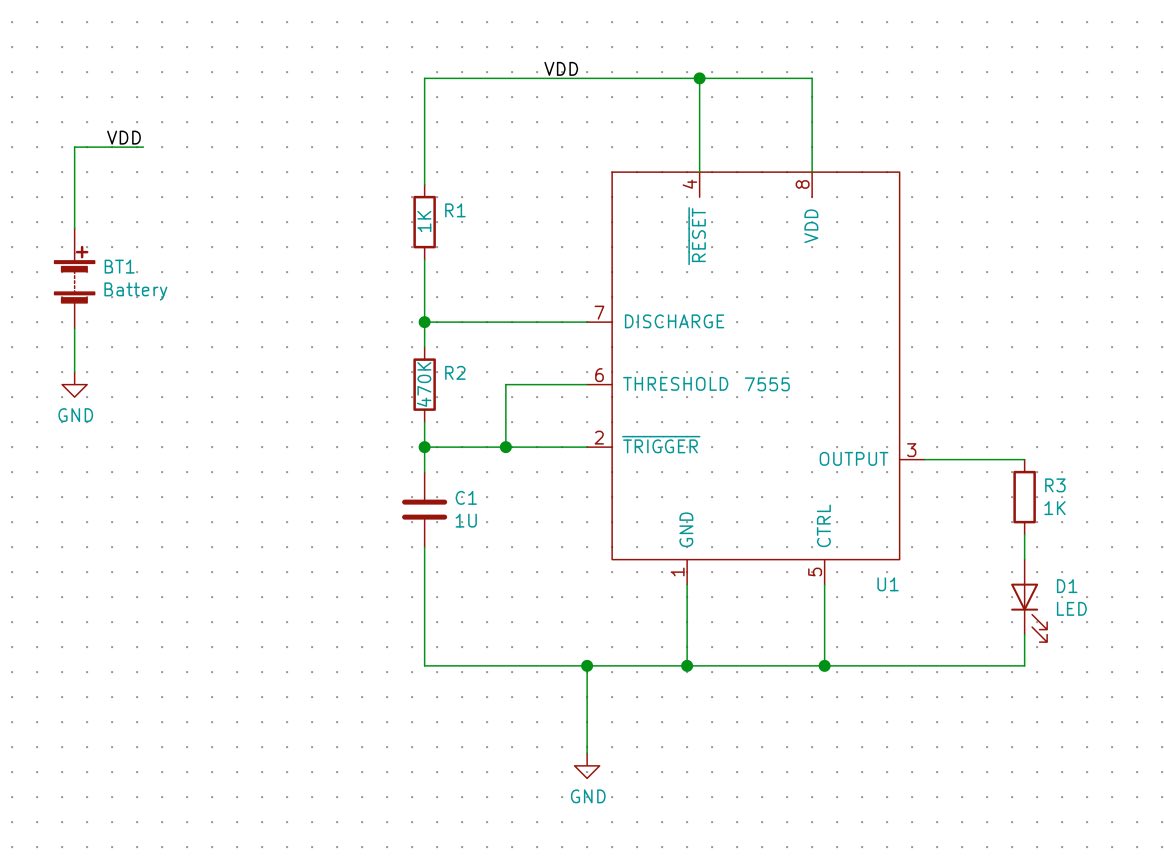
Designing schematic in KiCad
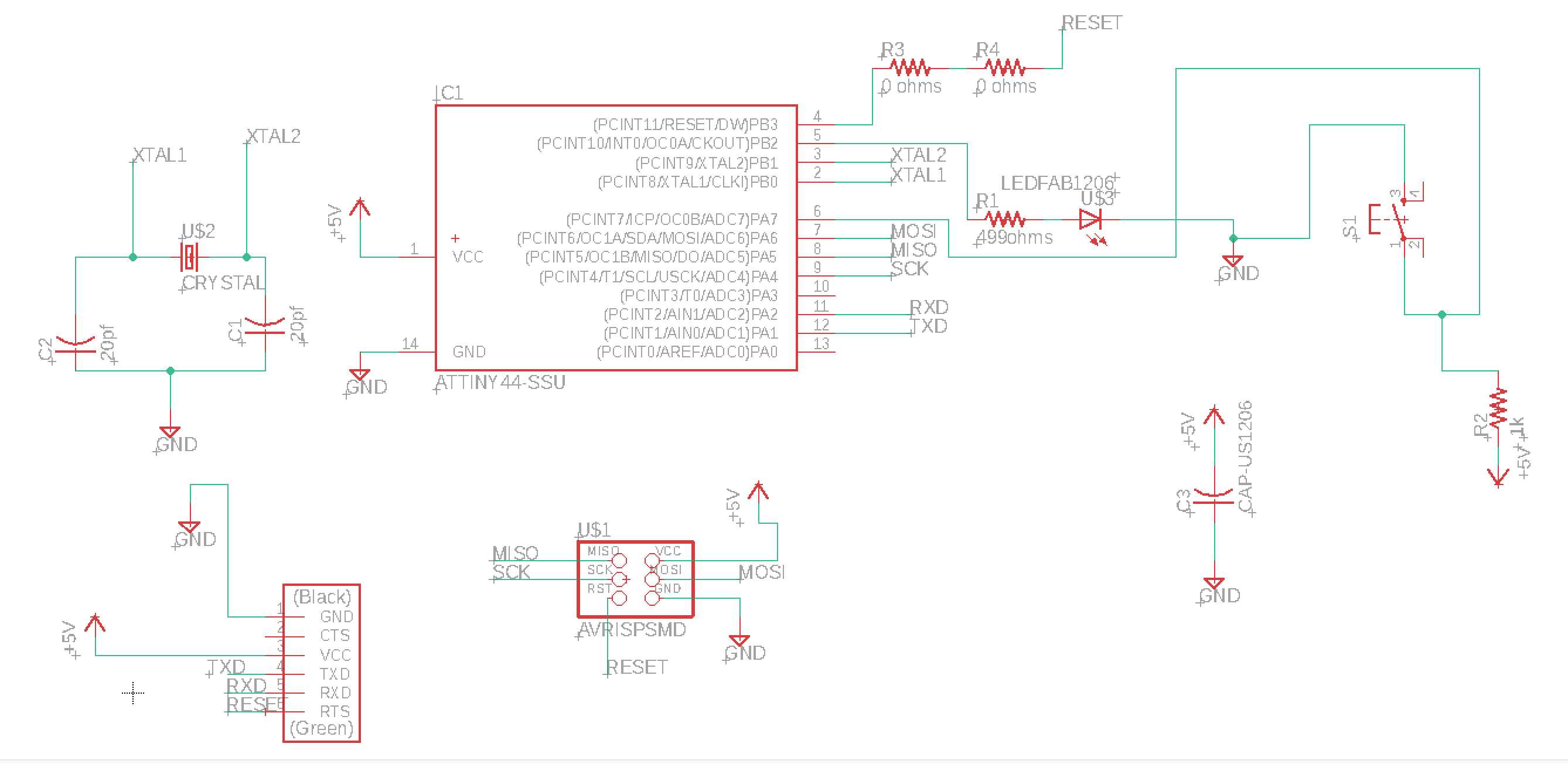
After importing the library and following darshan page i was able to draw below schematic.
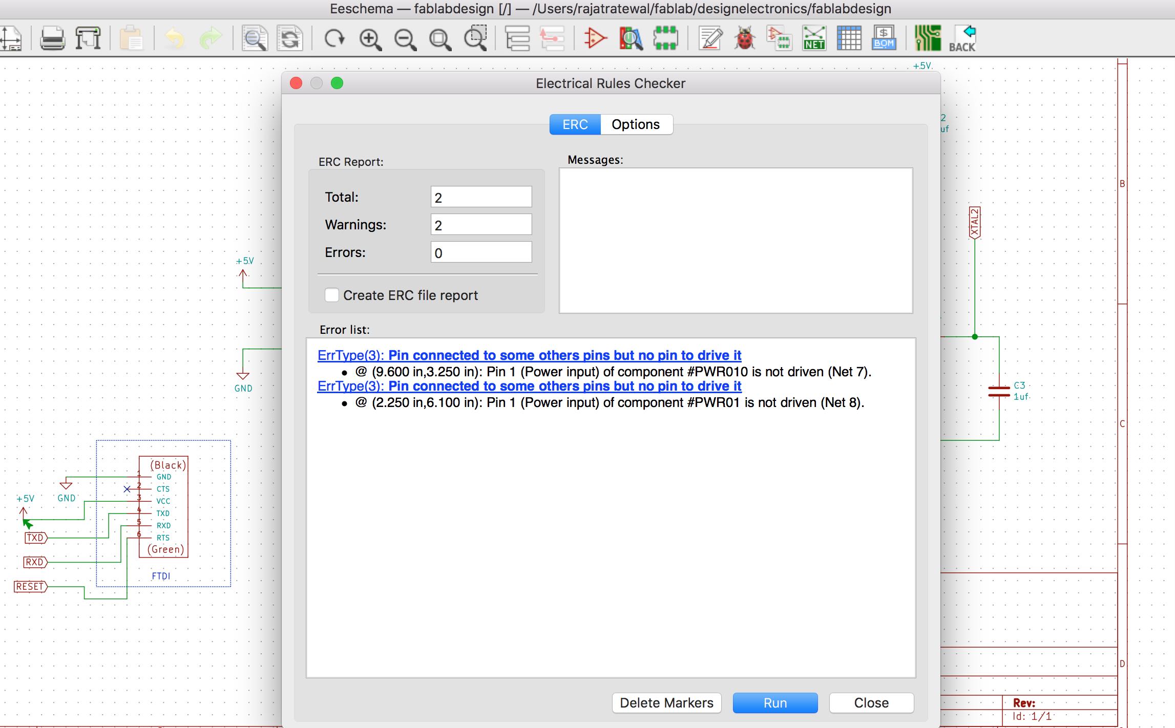
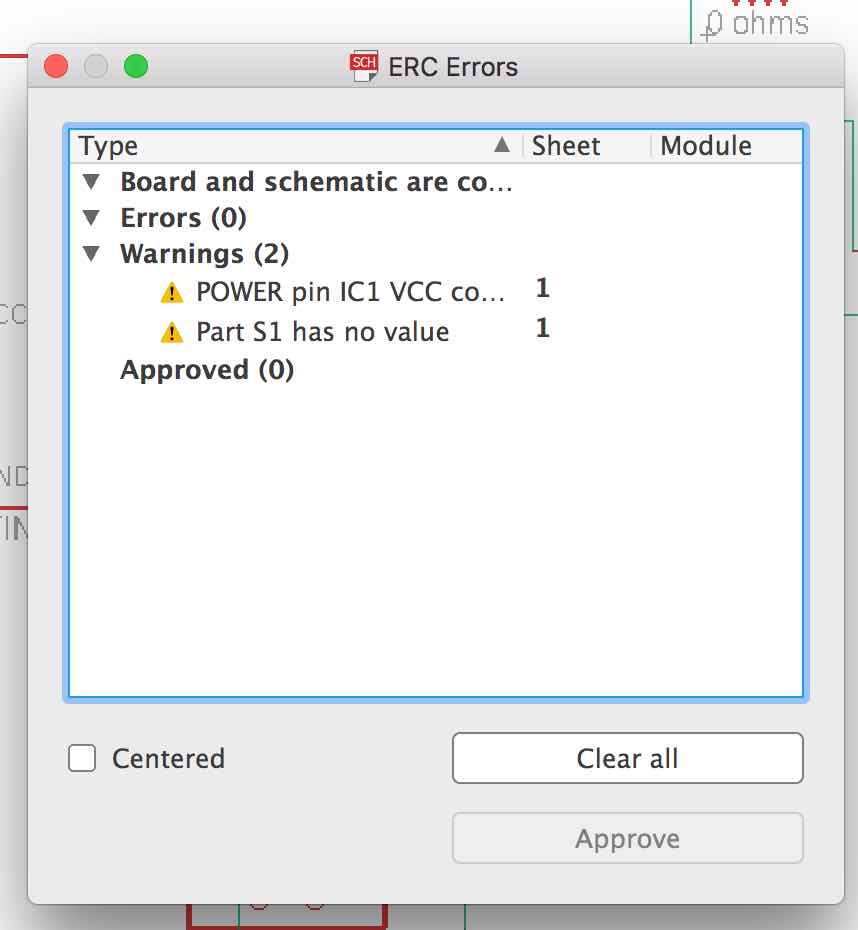
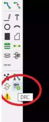
Electric Rule Check
One of the feature in Kicad is to check the schematic for any electrical rule error. So i tested that out after preparing my schematic.
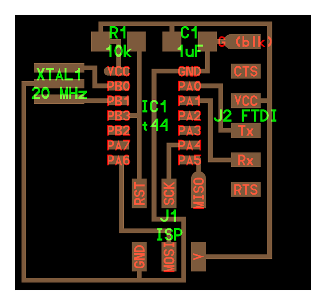
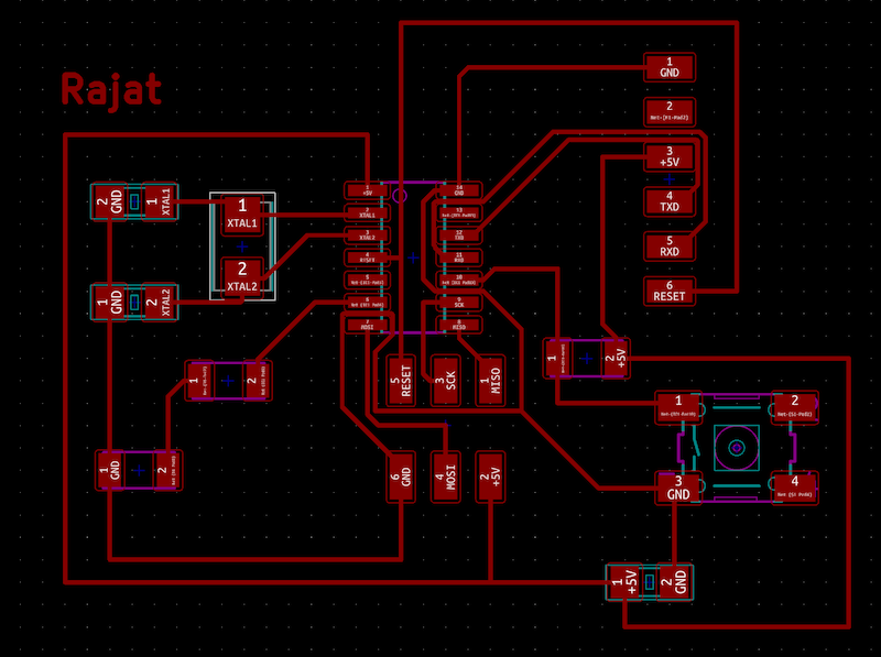
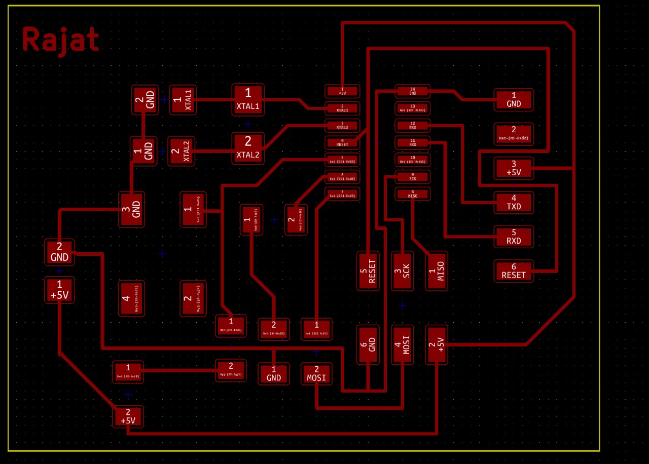
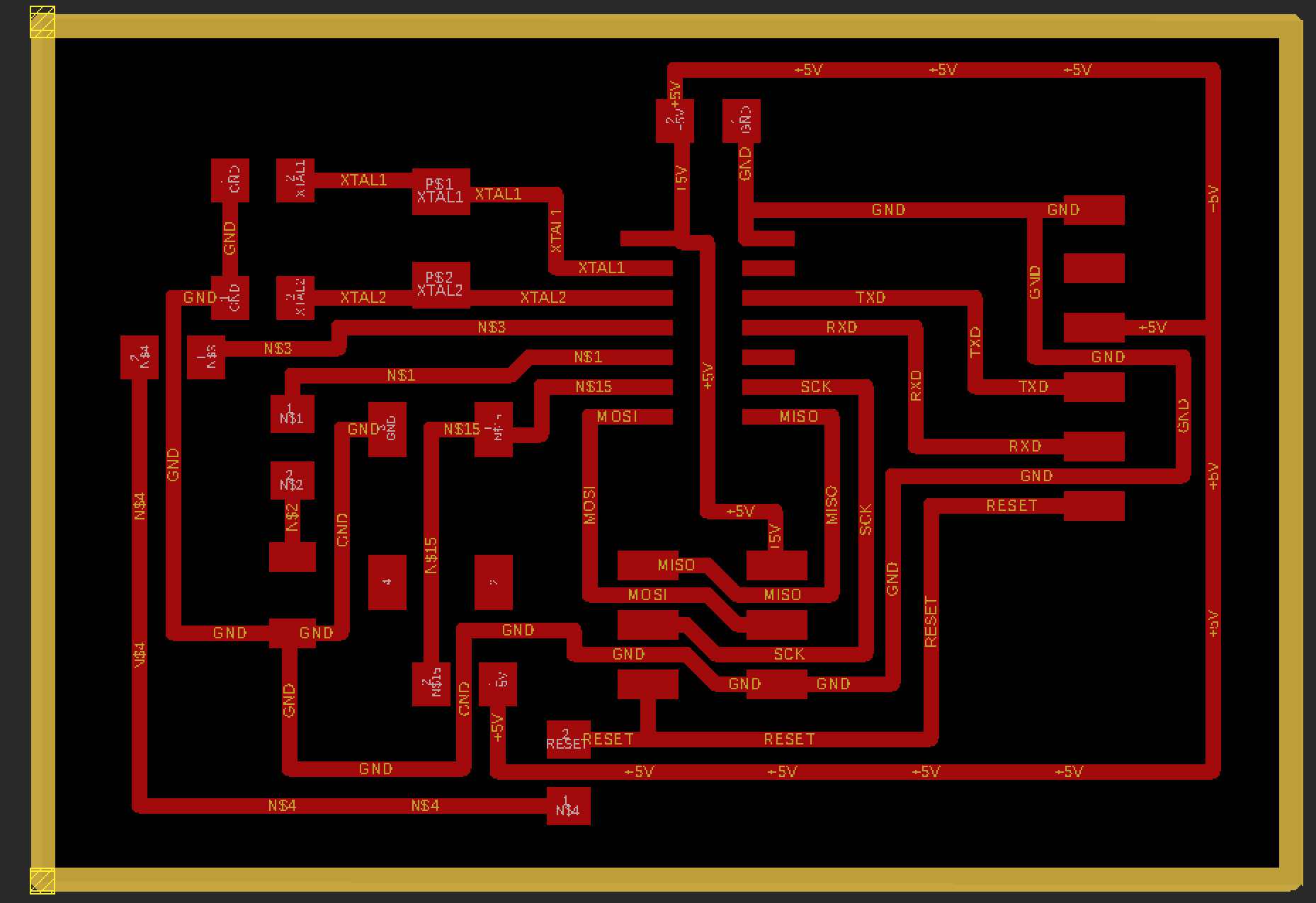
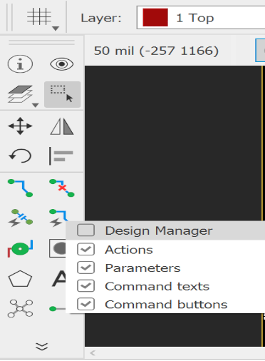
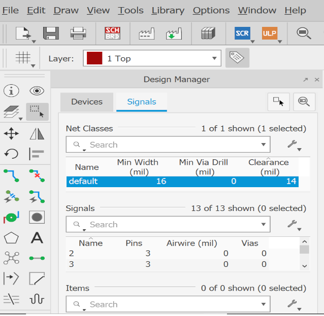
Routing the Board in KiCad
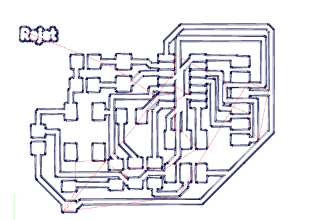
I spent most of my time in KiCad in routing this simple board. After many tries i was not successful in KiCad. Everytime it was left with one or two traces that were not feasible in a one sided PCB.
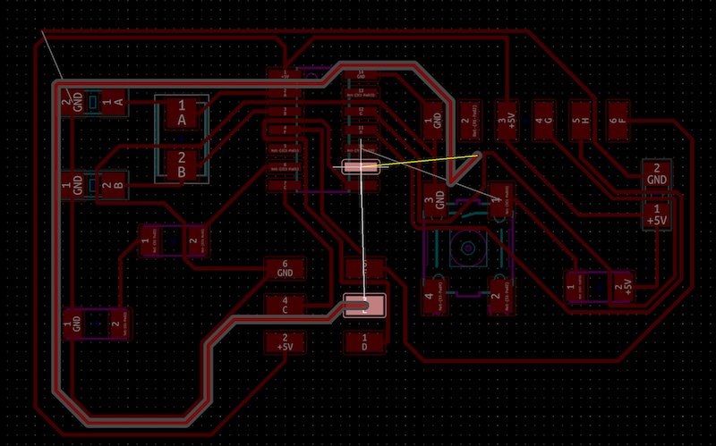
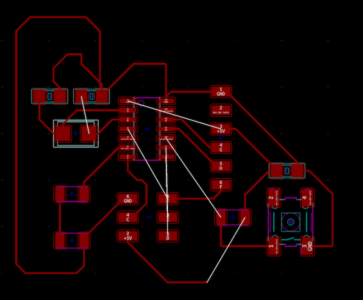
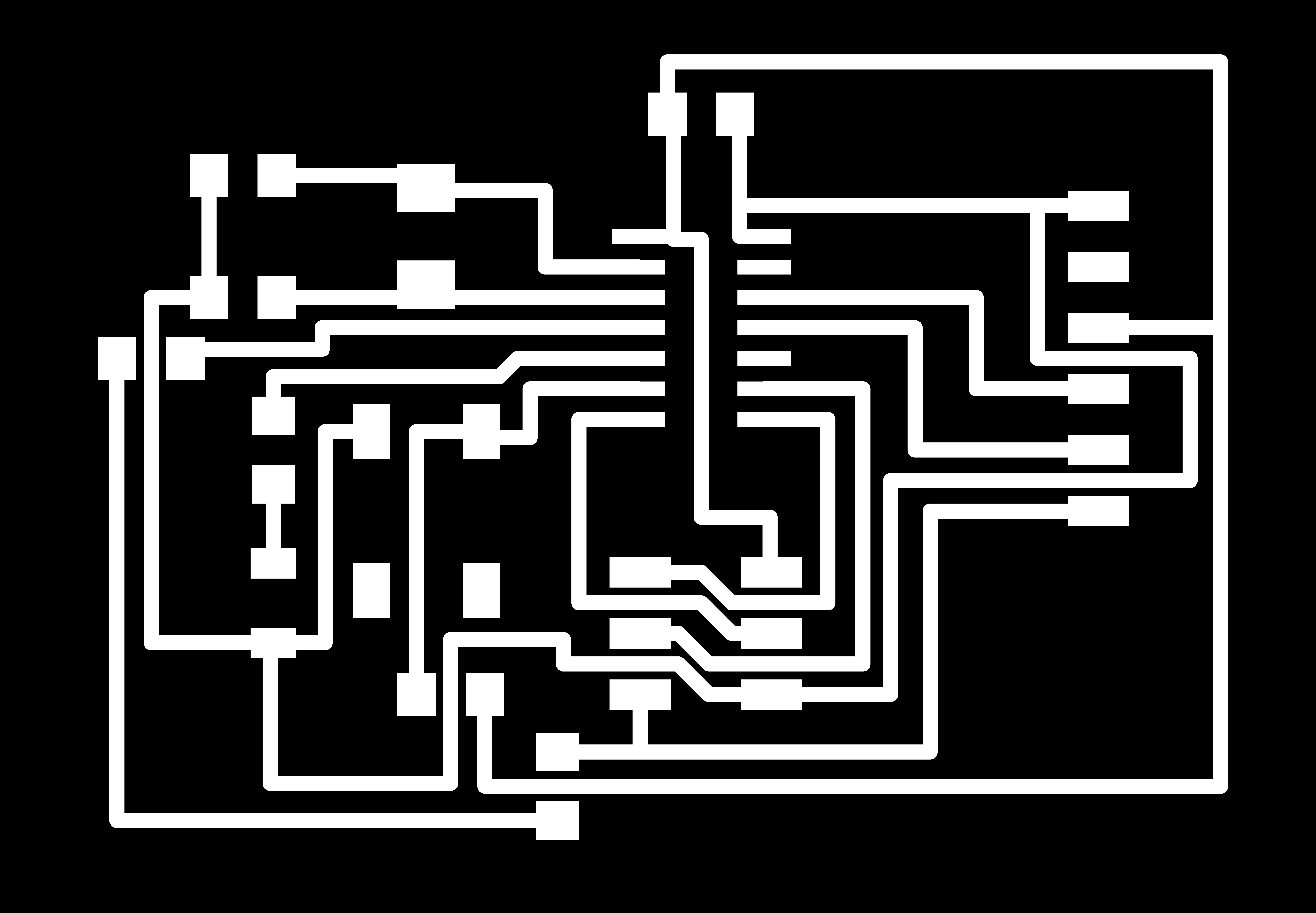
This was the best i was able to reach in routing
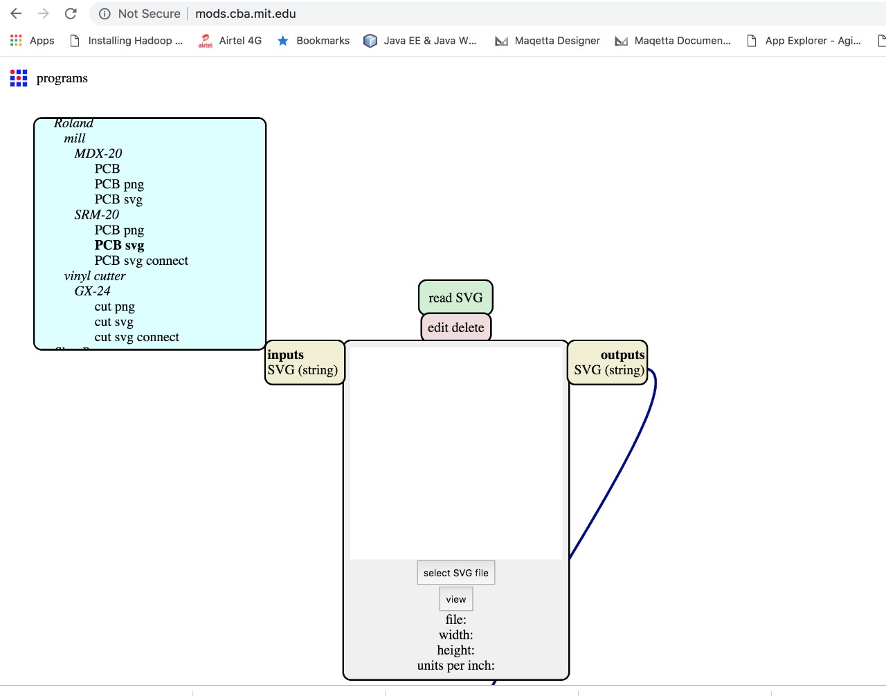
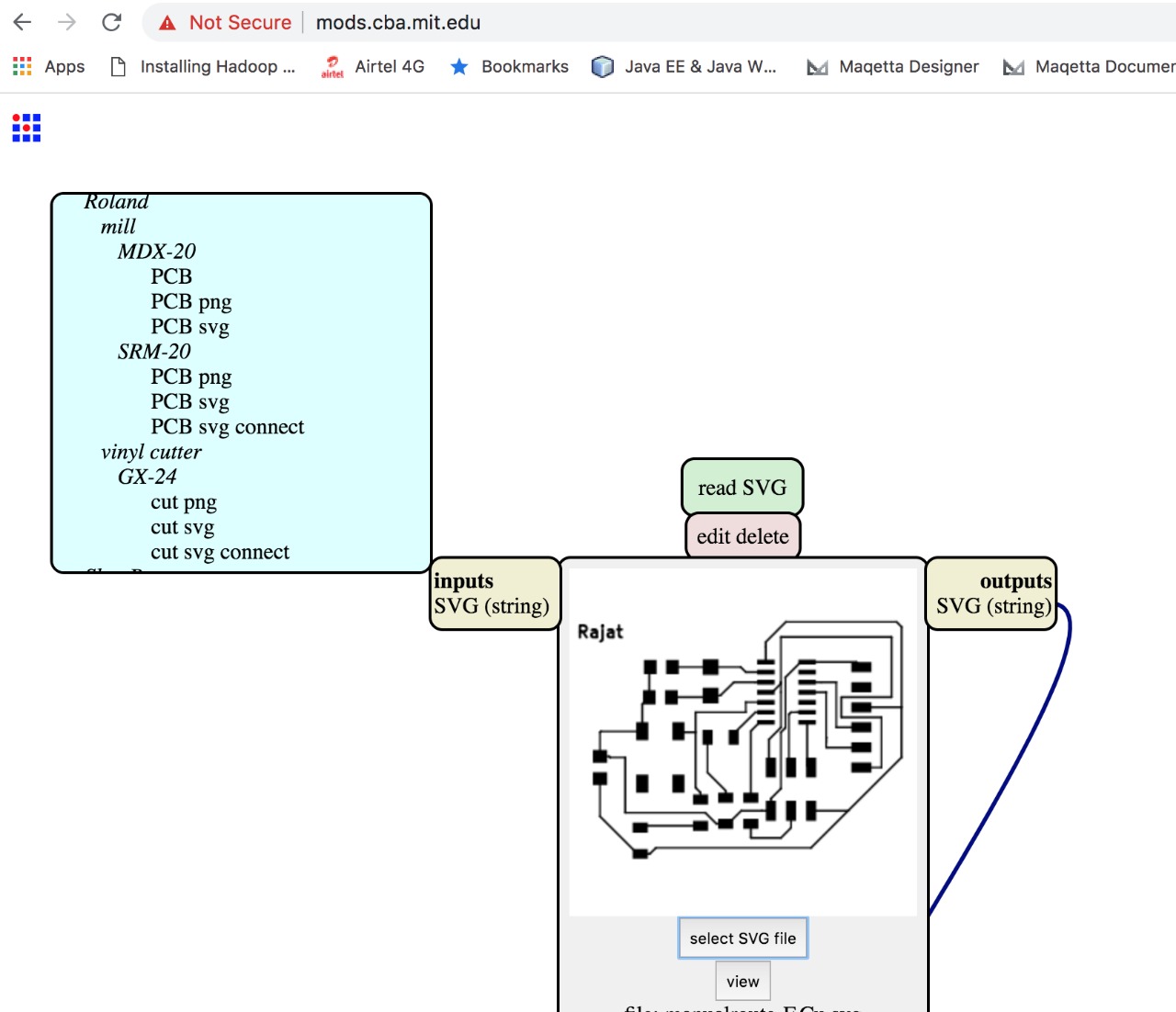
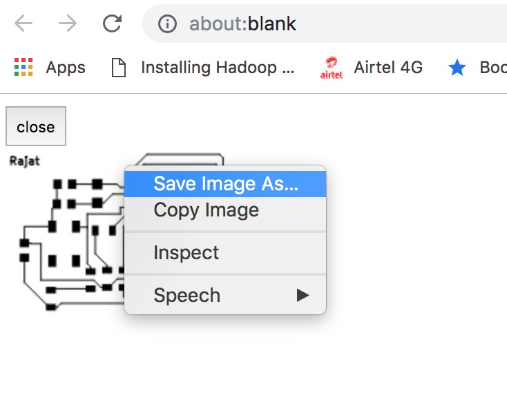
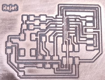
Using Mods to Create PNG File
After this i followed Darshan page but he was using Gimp to create the png file for milling. I remember Neil mentioning that we can do this by new mods. So instead of that i tried new mods to create png file for milling.
The process was pretty simple.
In mods you select the svg file created by KiCad and open it in mods and save it as PNG (FYI just follow video tutorial to understand how KiCad create the SVG file)
Issues I Faced in KiCad
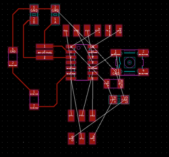
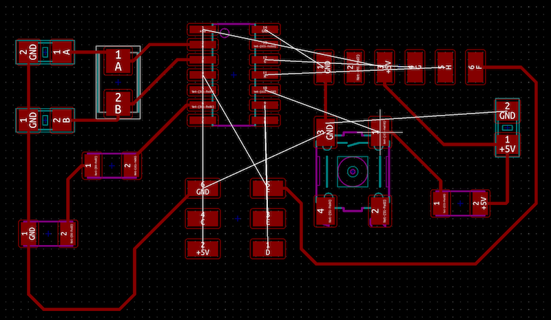
- After spending two days on failed routing, i finally called my instructor for help. Mr. Rahul gautam came for rescue, but he was Eagle expert. He asked me to draw the same schematic in Eagle and try auto routing option and mentioned that i can leverage 0 Ohm resistors if routing is not possible. When i investigated reason seems to be that we don’t have the right type of resonator/crystal and it was not aligned to diagram neil shared. Difference was that i had to add two capacitors to make it work the same hello board.

By this i learnt to use 0Ohm resistors but it was a waste of time. So before i started out with eagle i decided to give KiCad a try by changing the schematic by adding zero ohm resistors.
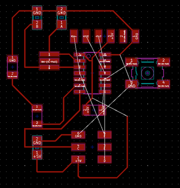
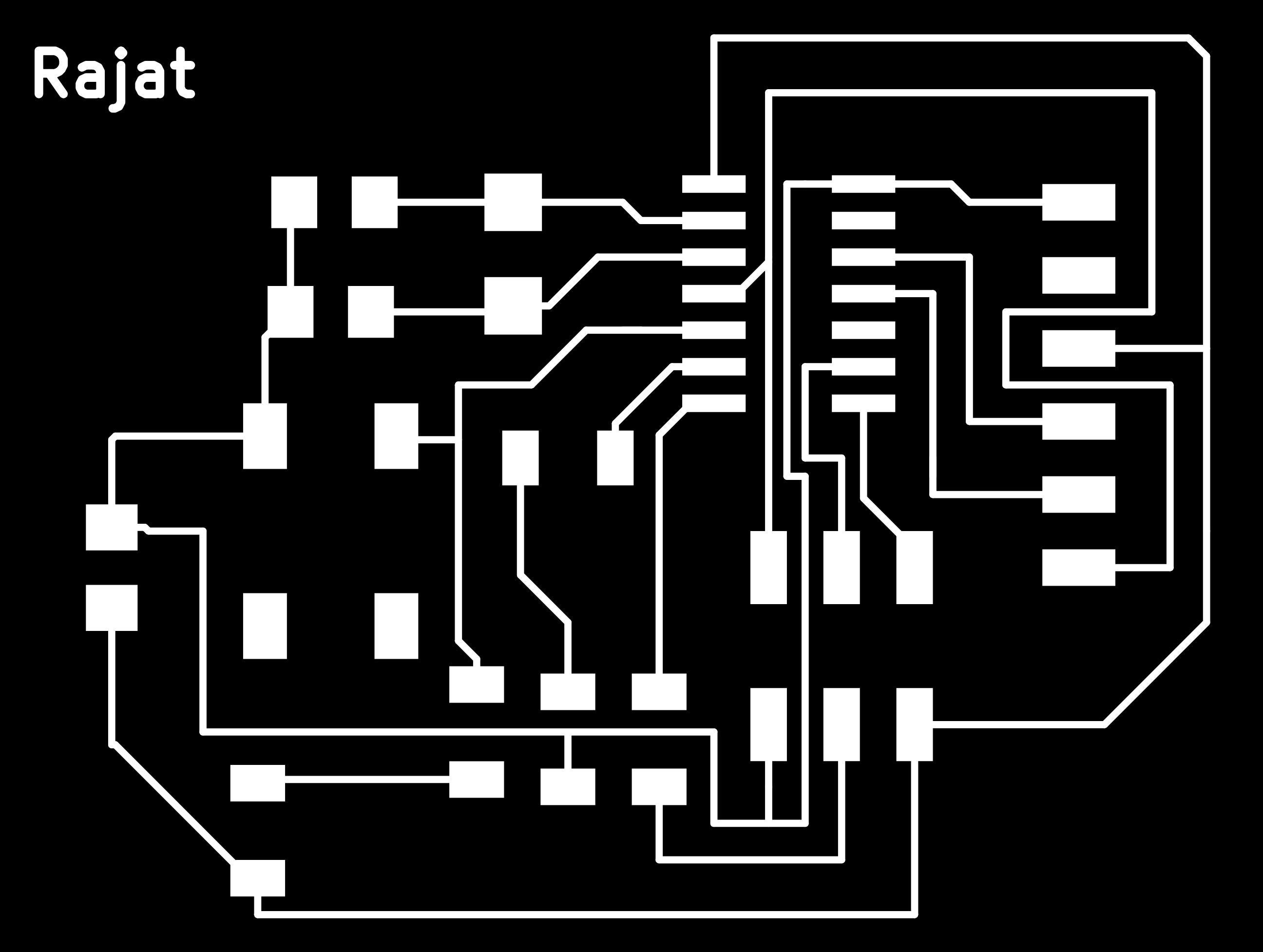
Once i added zero ohm registors i was able to do the routing easily.
- When i uploaded my files on fabmods to create toolpath i saw lot of traces overlapping which means board will not be milled perfectly so issue was with trace are not following proper design rules and spacing requirements.
So i realised the importance of using design rules before milling the board.
Download Files
Getting Started Eagle
Eagle is a PCB designing Software which is not fully Open Source but it can download it Under a student Licence and on the very basic ground it doesn’t makes an difference all the necessary options, tools are availabele in the education licenced version. It is avilable for all type of platforms.
So i started with some basics on eagle and found very good tutorial series on eagle PCB designing by Jeremy Blum
Once i was comfortable with basics of eagle i started with hello board designing. Eagle is quite widely used by electronics engineer so i wanted to spend good amount of time learning this software.
Designing schematic in Eagle
- By default, Eagle does not have a component library, so I downloaded eaglefab library and loaded it into the control panel window. The library contains the information of some components which include in addition to the technical characteristics, also the physical dimensions and the dimensions of the footprints.
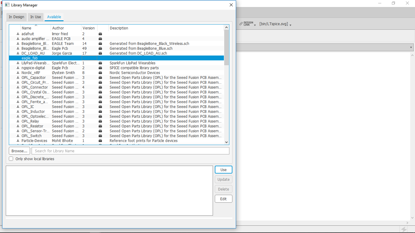
- Next is to use this library in my schematic, Click on Options-> Library manager. Click on the “available” tab and search for the saved library. Then click “use”
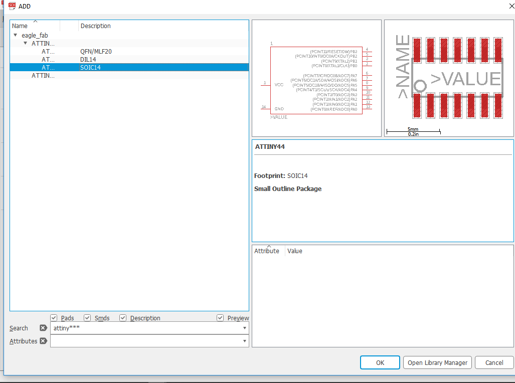
- Adding components , To add components to your schematic, select add tool. Now in the popped-up window, search for the required component and click OK.
- Next, wire all of your schematic symbols together with nets and add values and part names.
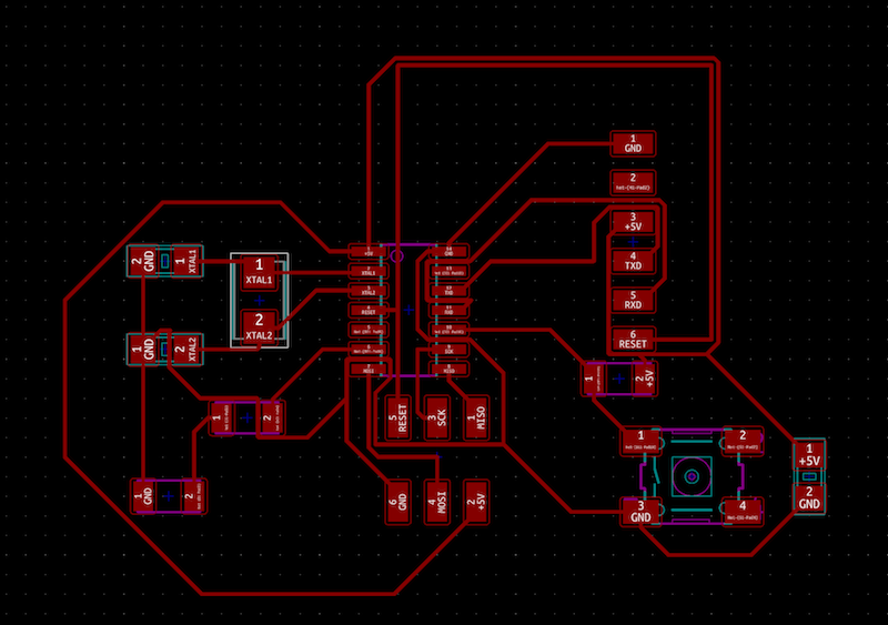
- Snapshot of final schematic
Electric rule check
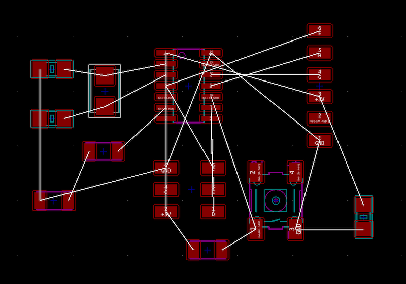
Routing the board in Eagle
Design rule check
When a DRC dialog box pops up, click on Size tab and set following parameters. You only need to set minimum track width as 20/24 mil (minimum 16 mil) as rest values are default and doesn’t matter as such. Then click on Clearance and set following parameters. Again you only need to set clearance in first column as 20-30 mils depends of much clearance you want in your design only as rest values doesn’t matter.Also one of the key points is to decide the trace width and clearence between pads and traces. For my design I kept the trace width of 16 mils and clearence of 14 mils. This is what i made mistake in KiCad causing issue in Mods when i was creating toolpath
Download Files
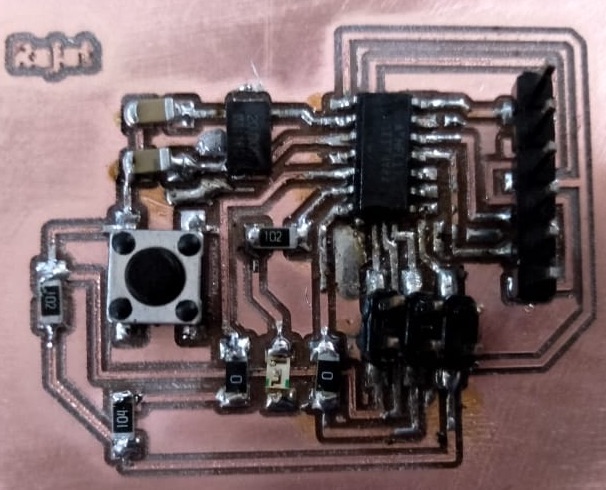
Milling and Soldering
So finally i got my PCB milled which i learnt in electronics production week.
Before solder
After Solder
Group Assignment
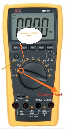
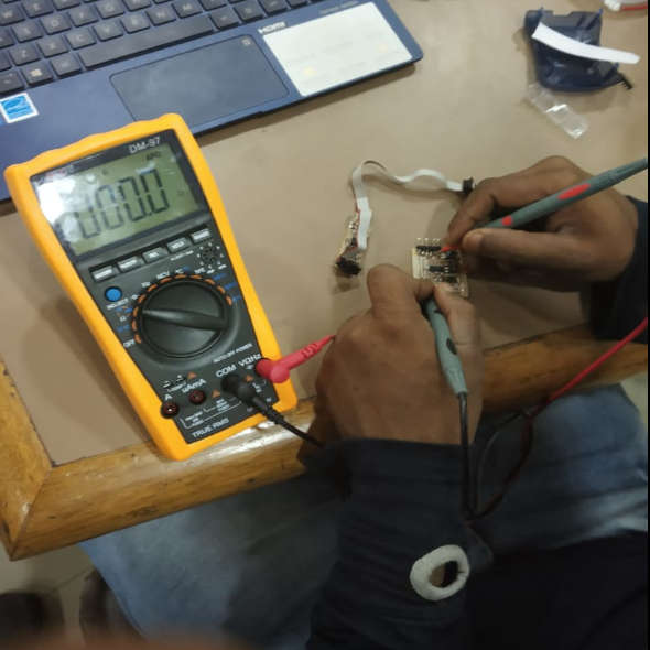
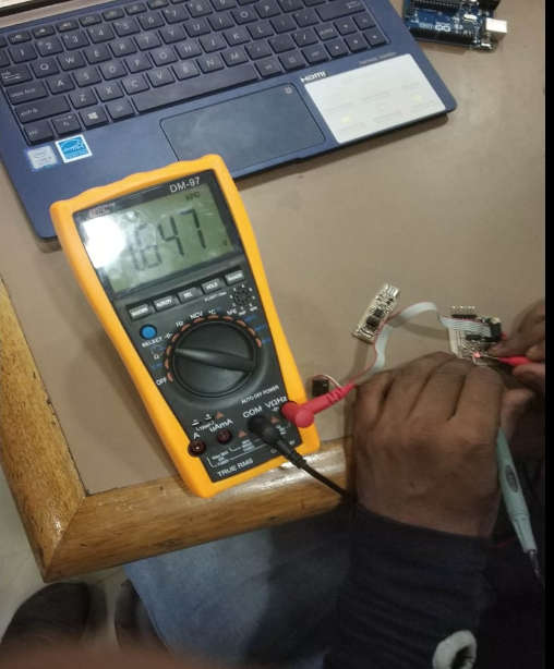
Understanding Multimeter
We use the mutimeter to test the continuity of my circuit as well as to check wheter the proper volatges were being received across he components. Our group assignment was also to test the microcontroller board with a test equipment in the lab we understood multimeter functions and limitations and how to measure voltages, current and continuity.
-
Continuity mode means: If the probes are connected—either by a continuous circuit, or by touching each other directly—the test current flows through. The screen displays a value of zero (or near zero), and the multimeter beeps. Continuity! If the test current isn’t detected, it means there’s no continuity. We use the VCC (red cable) and GND (black cable). This is indeed a very important aspect and a basic concept for testing all types of PCB’s.
-
Testing for continuity at various traces and soldered components
-
Testing the leds to turn them on via multimeter probes
Understanding PowerSupply
In our lab we have Scientific PSD3005 0-30V 5 Amps Power supply which has following features.I used this power supply to power up my board via Vcc=5v and GND.
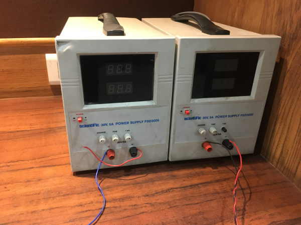
- DC 0 to 30V, 5A
- Constant voltage & constant current operation
- Digital displays for voltage ¤t
- Adjustable current limiter
- Protection against overload & short circuit
Understanding Digital Oscilloscope
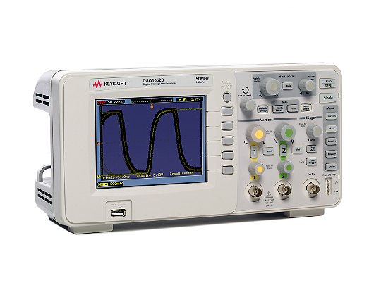
This week we don’t had DSO available in lab, i have documented usauge of this instrument in week 11 Input devices. You can refer below link to get more details.Week 11 Input Devices
Overall Learning Outcomes
- Very easy to understand design softwares especially if you watch youtube videos shared above
- Routing is an Art, you need to understand layout and components before you start drawing randomly. I am not expert in electronis design so i struggled a lot in this
- Clear segregation of PCB, Schematic making both Kicad and Eagle a modular software
- I learnt a great deal about how to use Multimeter