7. The Design of Electronic Circuits
Goal(s):
- Group project:
-
Use the test equipment in your lab to observe the operation of a microcontroller circuit board
-
Individual project:
- Redraw the echo hello-world board, add (at least) a button and LED (with current-limiting resistor) check the design rules, make it, and test it
- For extra credit: simulate its operation
Introduction
The main aim of this week is to learn about different electronic CAD softwares, identify one of them for our electronic designs then, redraw the the echo hello world board and make it. I had used Eagle and EasyEDA for the design and production
PCB Designing
A PCB(Printed Circuit Board) mechanically hold and electronically connects the components using conductive tracks(Copper). There are different types of pcb’s starting from Single side to multi layer pcb’s. Since we are using milling machines we can make maximum double side pcb’s in Fab Lab. The crosssection of the single side and double side pcb’s are showed below. The copper layer is used for connectons between the components. The layer below copper layer is called substrate layer, substrate is made using fiberglass-epoxy laminates,Teflon,ceramics etc. We are using a pcb with FR (Flame Retardant), a fiberglass-epoxy laminate. In multi layer Pcb’s multi layers of FR is laminated togather. There are different grades of FR; FR1,FR2,FR,FR4 etc.
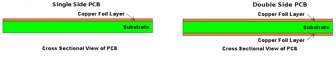 - PCB cross section
Flame Retardent 1 (FR1)
PCB Substrates are specialized materials that do not conduct electric currents. They serve as a laminated electrical insulator between circuitry, An electrical insulator is a material whose internal Electric charge do not flow freely, and which therefore does not conduct under the influence of an each layer of circuitry, consequently, is connected through plated through holes to connect traces on opposite layers. FR-1 is a hard, flat material that consists of a thin layer of copper over a non-conductive phenolic paper copper-clad. FR-1 is primarily used for making circuit boards. The thin copper layer can be milled or etched away, leaving traces to which electronic components can be soldered. Substrates requires electrical,mechanical,and thermal properties. I have gone through some documentation on different pcb’s and if any body interested can go through this link
Is FR-1 safe?
Unlike FR-4, which is fiberglass-based and generates dangerous glass-shard dust when milled, FR-1 is safe to use if you keep it away from your eyes, lungs, and skin. It is recommended vacuuming up the debris after the milling. Typically specified to 105 °C, some grades rated to 130 °C. Poor moisture resistance, low arc resistance are some features of the FR1 material.
PCB Design
PCB design is usually done by converting our circuit’s schematic diagram into a PCB layout using PCB layout softwares. There are a lot of open source software packages for PCB layout creation and design is available now, both open source and licensed. In this week i am planning to familiarise with these softwares.
123D Circuits Eagle Easy EDA Altium Proteus
PCB design and layout process
The first process of PCB design starts with circuit schematic design, using any one of the softwares we can design the circuits. Each software will have a schematic design tool for this. We can draw our circuit schematic by pick and placing the components available in the library, interconnect it using wires. Once completed the schematic the next process is routing of pcb, the PCB software routes the physical connections on the board according to the netlist from the schematic. To achieve this it will use the number of layers that are available for connections, creating via holes as required, but in our case maximum double layers is only possible with the pcb modela milling machine . Autorouting and manual routing provisions will be available in softwares, also we can check the design rules at different stages. After completing the routing we can use the output to make the pcb,noramally most softwares the output will be in the form of Gerber files. It is an open ASCII vector format for 2D binary images. It is the standard used by printed circuit board (PCB) industry software to describe the printed circuit board images: copper layers, solder mask, legend, etc. Since we are using mechanical etching the output required will be in the form of images(.png).
PCB Design
Being a complete newbie at Electronics design and having only seen and heard about board design, there was a huge learning curve for me, but with the help of in-house members and some advice from the local Gurus, there was a itemized series of steps that had to be followed for the completion of the assignment.
- Designing a circuit board
- Observing Board operation
- Redrawing the Hello World board
Designing a Circuit board
For this exercise, I used an online tool called EasyEDA which was really simple to use for both schematic and circuit development.
Since Electronics was new to me, I decided to relook at the FabISP Circuit and redesign it for ease of soldering and operation
Using EasyEDA was as easy as its name suggested
I started by making the Schematic of a target board (FabISP Tiny Star in this case) which took close to 3 hours as I had to figure out all the key elements of the software.
Preparation of the final PCB was as simple as clicking the Convert to PCB Option and getting the traces autorouted as per the internal algorithms for the circuit.


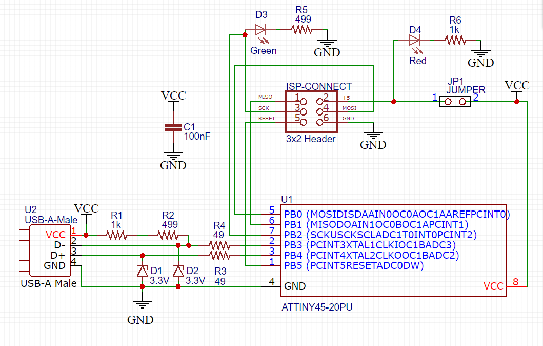
Redrawing the Hello World Board
From the archive page, I took the schematic and modified it for the ATTiny85 chip as per the following steps to redraw the board from scratch and by using the EasyEDA Software used earlier.
Component List
I will be using the following components to make the Hello board.
One Attiny85 microcontroller One 2x3 Programming Header One 1x6 FTDI Header One 499 ohm Resistor Two 10K ohm Resistor One 10uF Capacitor One LED - Add on to board One 6mm Switch button - Add on to board
Board Design
Using the board designs created from Fab Academy Archive in the EasyEDA software, I used the following schematic to convert into a PCB board for preparation.
 Schematic
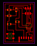
 Board
Board
 Final board
 After changing the track width to O.6mm to allow for proper laser and chemical etching.
Completed Hello World Board
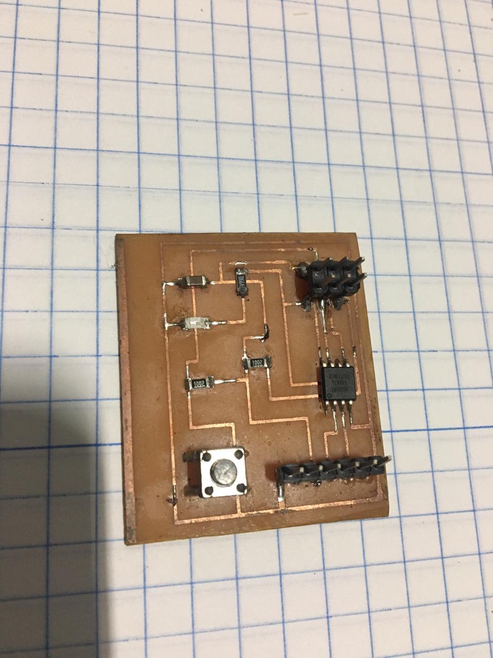
Download the files from here
Program and Test the Hello board
I used the Arduino Uno as ISP to program the Attiny85. I followed this guide to setup the Arduino as ISP and the Attiny85.
Connect Arduino UNO to Attiny85 as follows
Uno –> ATtiny85 10 –> Reset 11 –> MOSI 12 –> MISO 13 –> SCK 5V –> VTG GND –> GND
With reference to Program ATtiny and Programming ATtiny85. The following is the steps to test the LED and Button program
Testing LED with Arduino Blink Program
Run Arduino IDE and load Blink from Example > Basics Go to Tools, ensure that the following are selected Board: ATtiny25/45/85 Processor: ATtiny85 Clock: Internal 8Mhz Port: COMXX (COM1 or COM3 depends on the port detected) Programmer: Arduino as ISP Compile and upload Note the pin used for LED from schematic and declare as output pin, in this case is PB1 If successful, the ATtiny85 LED should blink with interval of 1 sec

My program is available here
Testing the Button using Arduino IDE
Run Arduino IDE and load Button from Example > Digital Board: ATtiny25/45/85 Processor: ATtiny85 Clock: Internal 1Mhz Port: COMXX (COM1 or COM3 depends on the port detected) Programmer: Arduino as ISP Compile and upload Note the pin used for LED/Button from schematic and declare LED as output pin and button as input pin, in this case LED as PB1 and button as PB0 If successful, the ATtiny85 LED should goes off when the button is pressed

My program is available here
Learning
This weeks learning was quite intensive and filled with lots of anxiety as I was designing and making boards for the first time and every time each wire was put into place and power given, I was expecting the boards to blow up and burn. Thankfully, this did not happen and we were able to program the boards and get it to do what we wanted quite easily. This exercise has made me feel mor confident in my abilities for soldering and programming boards as I can now see various possibilties for application of programmed boards.