Electronics Design
Group assignment
Class Week 6Individual Assignment
Two weeks ago we learned, that the ATtiny44 has no bootloader section in it's flash memory (see also ATTiny Datasheet, p.159). This means, that programing the microchip requires an external device, as e.g. an USBtinyISP, or the FabISP Programmer from our assignment week 4. The FabISP can be programmed via the Serial Protocol, but it is also possible to connect it to USB.
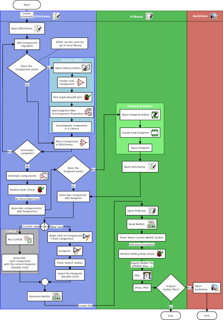
This week we designed the board with the KiCad programm, which is an open source software suite for Electronic Design Automation (EDA). The KiCad homepage shows a flowchart, which schematize the workflow of this software:
Installing the FabLibrary
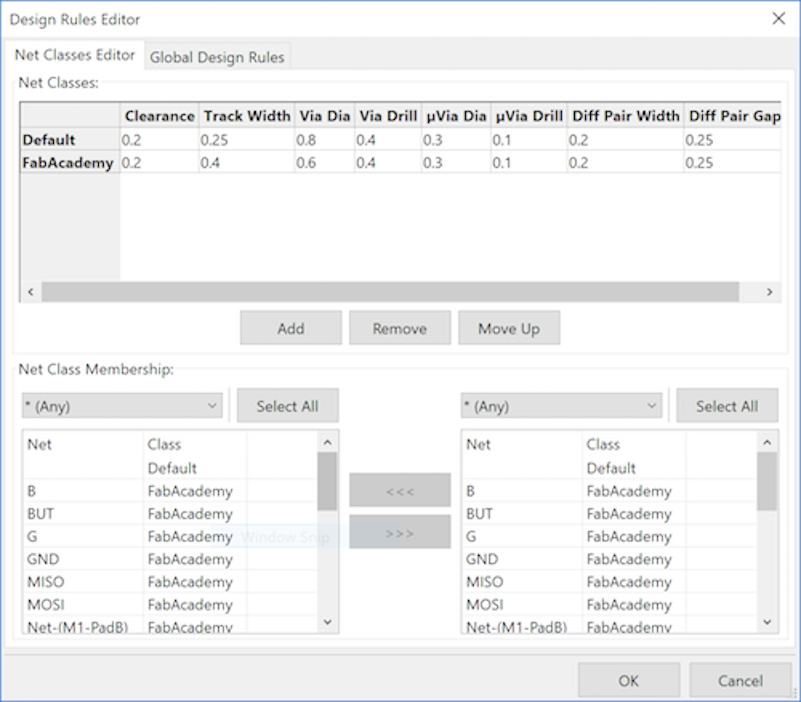
Before starting with the PCB design, I had to install the FabLibrary. For that I opened the Design Rules Editor and made up the settings as shown here:
Circuit Design
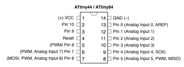
The PCB had to be feeded via the FTDI connecter, so while designing the board I had to make sure, that the pins are well connected. For that I also used the schematic of the ATtiny44 pinouts.
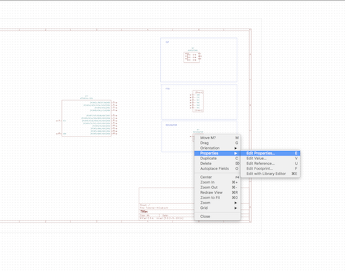
I began to design the circuit by creating a basic structure, placing the main components into marks and defining their properties.
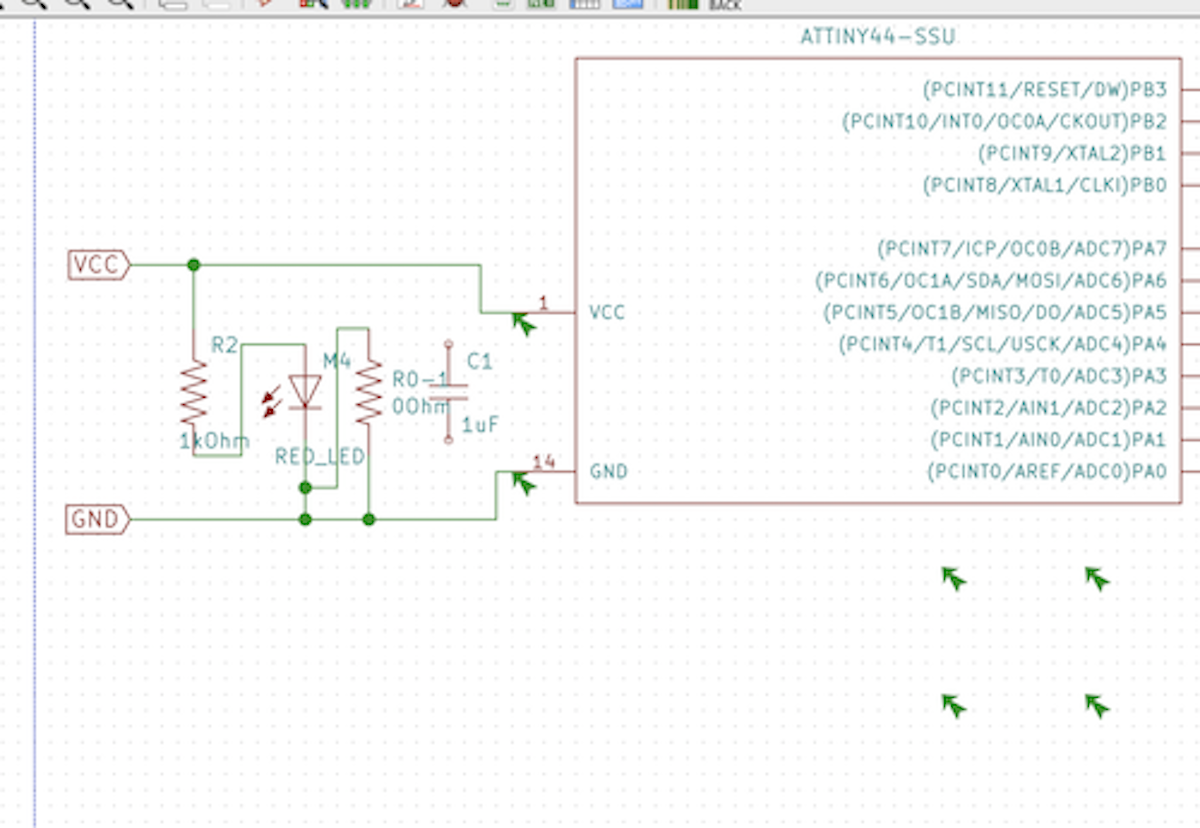
Here I added a LED circuit to the board, that will light up, when the PCB is going to be connected to the power:
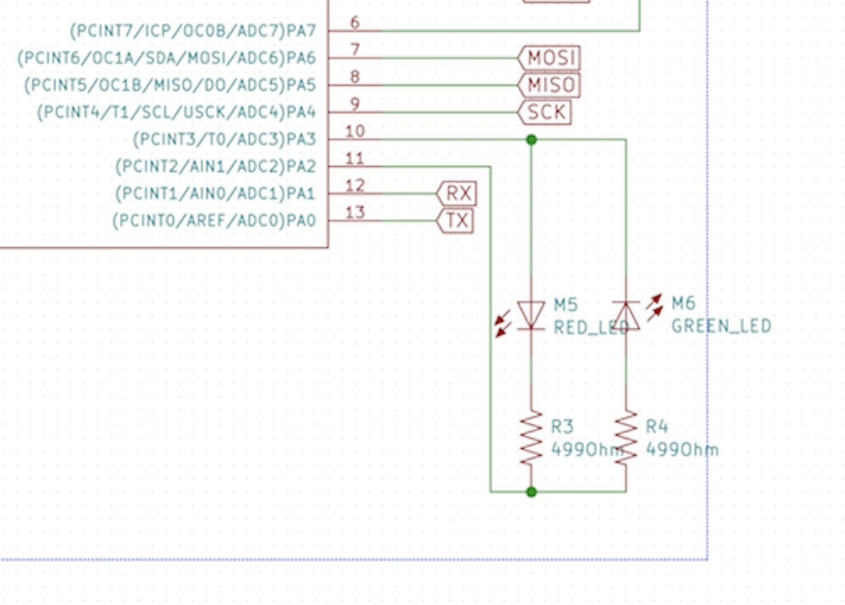
Then I made an other circuit with two LEDs, a green and a red one. I placed them parallel to each other, but with opposite directions. This constellation in its simmple form is also named as the Charlieplexing technique (see also Wikipedia).
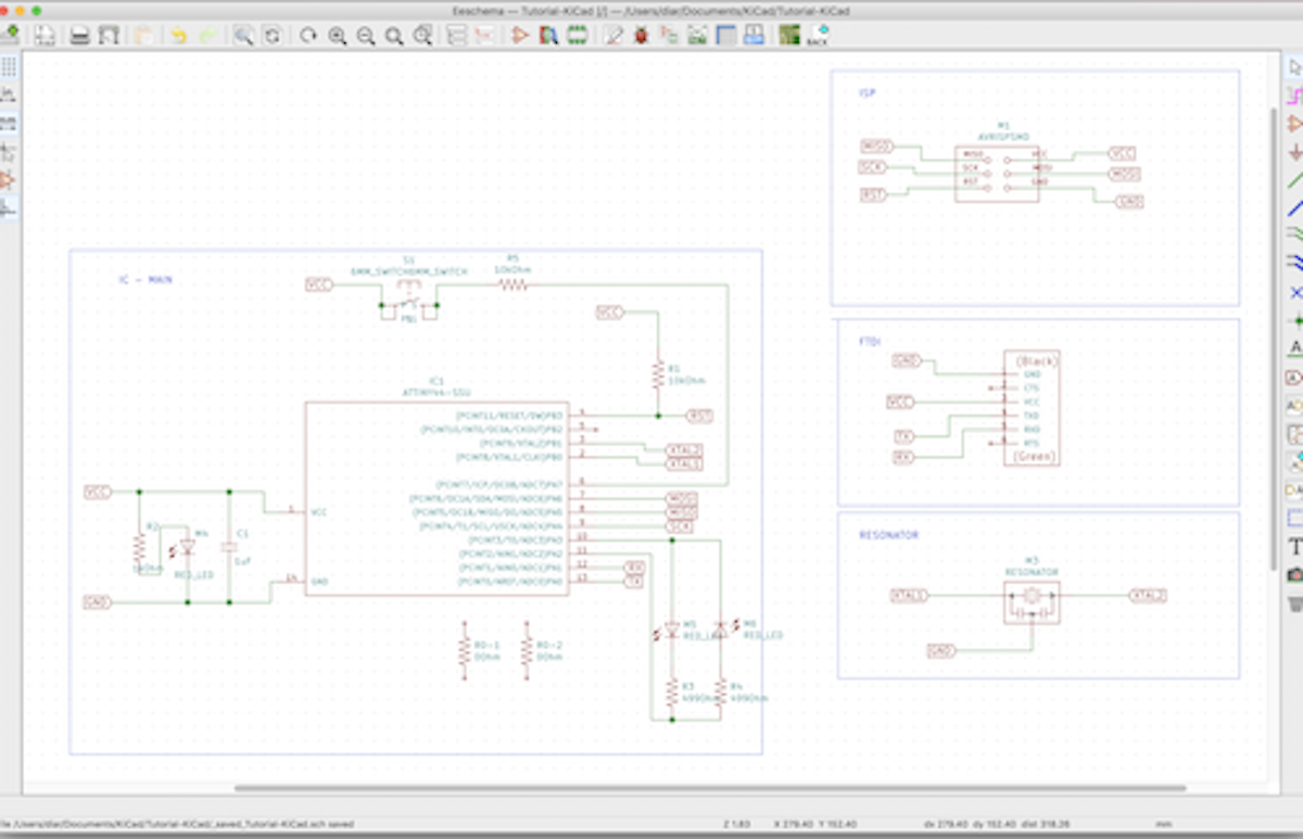
Now the Schematic Layout Editing was finished, ...
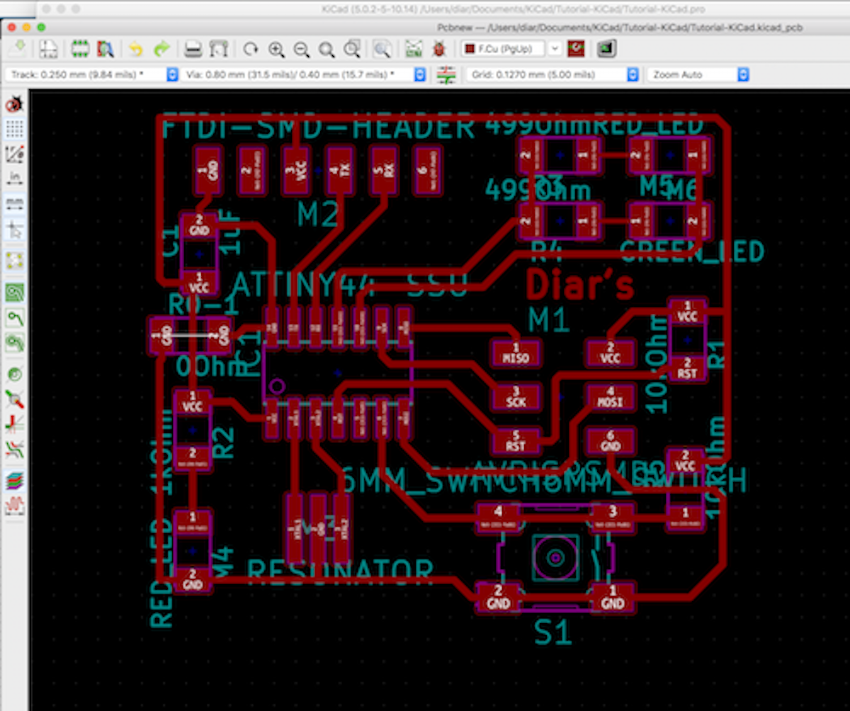
... and I could switch over to the PCB Layout Editor. My next steps were: routing the traces and optimizing the spatial extension of the circuits. After this I used the "Inspect/Perform design rules check" tool, to see if everything is virtually well connected.
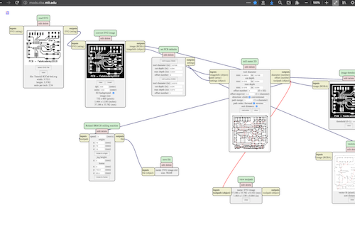
Then I had to export two SVG files, one for the traces and one for the outline cut. These files were sent to the MODS interface...
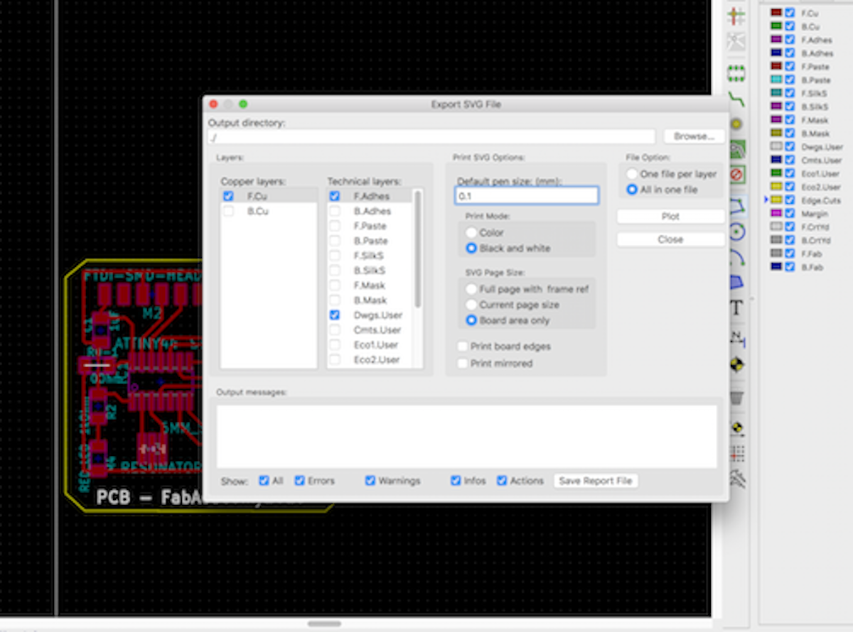
... to generate the RML Codes for both layers:
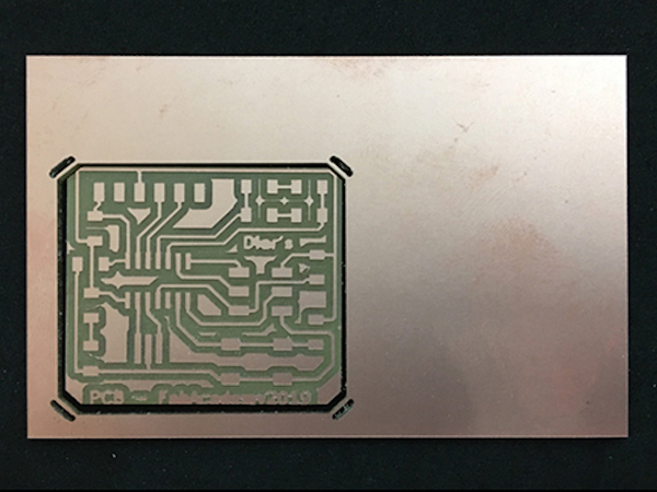
Using the Roland SRM-20 machine I milled first the traces and then the outlinecut.
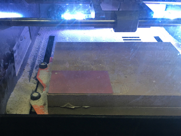
The milling went good, but I forgot to consider the mill thickness, when I estimated the outline trace.
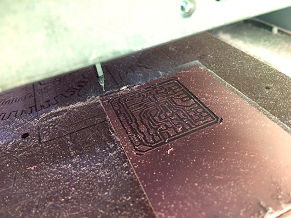
The mill was cutting also in the inner part frame line, in reference to as it is shown in the Layout Editor. As a result a part from the text on the PCB has been cut away by the outline cut.
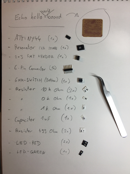
The board was ready to be soldered, for that I prepared the Bill of Material (aka BOM):
After the soldering the PCB was almost finished.
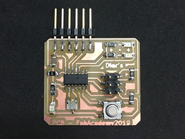
The circuits and also the soldering of the components needed be tested with the Multimeter, to make sure that everything is well connected. At least the test was successful and the PCB ready to be programmed.