Hello World Board
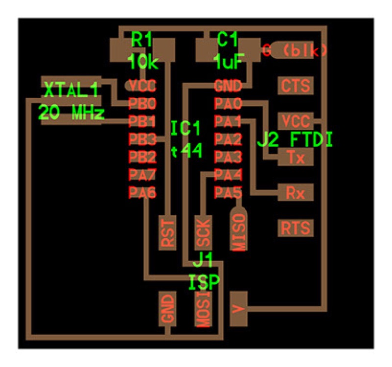
I am redrawinng the hello.ftdi.44 board (Credits : Neil ) The scheme I reffered is as follow:
Components
The basic components required are :
The additioal components required are :
Pin-out
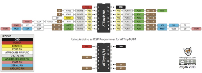
I have used ATtiny44-SSU for my Hello Echo Board. I have refered pinout and data to understand what goes where in microcontroler.
What Data Sheet does is that it helps to find out :
What voltage a part needs to run?
How fast a part will run?
How to communicate with a part?
To learn more about data sheet and configuration I referred following links:
What did I learn from reading Data-sheet?
As I have read the datasheet here I will list down all the things that are important and how does it help ? :
Why Did I choose AtTiny 44 for Hello Echo ?
The simple hello echo board that I wanted to make doesn't run on heavy sized program. Thus AtTiny44 Memory is enough to perform that.
What pin does what ?
Here I have poined out what pin is for what :
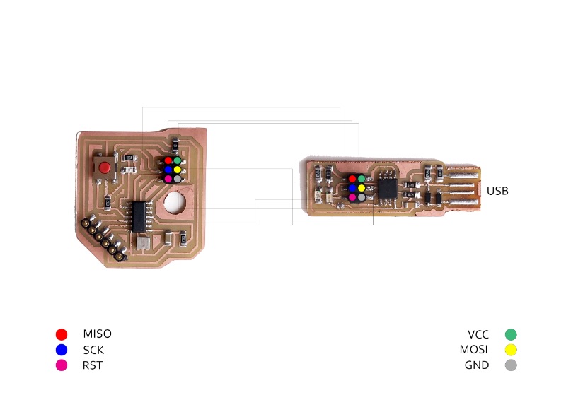
I used MISO, MOSI, SCK, RST, VCC, AND GRD pin for standard 6 pin header programmer ISP.
XTAL1 and XTAL 2 was connected with ends of Oscillator in my board.
SCK was connected to LED as Power LED and drives LED while programming.
(*Refer to port and circuit diagram for particular to decide on which pin to use where for further reference.)
Pinout of ATtiny 44/84
Note : You can identify number of pin using the notch on microcontroller.
Understanding the Circuit
First of all from Schematic annd reffereing various diagrams I tried to draw schematic on paper.
After a bit of confusion I figured out followiing connections.
What did I figure-out from the Circuit?
From the data sheet and reference of neil's board I figured out following things and made the circuit.
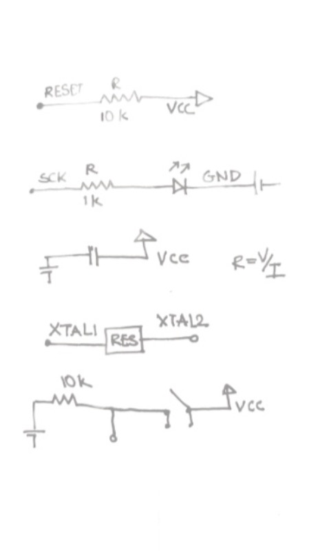
1. Crystal/Resonator was connected to XTAL pins. Which in the microcontroller acts as Chip Oscillator pin.
2. SCK is used while programming and it is connected to SCK pin of microcntroller, other node gets connected to Ground. SCK will be conrolled in program and will blink on basis of code.
3. Current Limiting resistor is resistor is used to limit the current through the LED and to prevent that it burns. If the voltage source is equal to the voltage drop of the LED, no resistor is required.
4. Pull-up resistors added to prevent unknown state in MCU.
( MCU with one pin configured as an input. If there is nothing connected to the pin and your program reads the state of the pin, will it be high (pulled to VCC) or low (pulled to ground)? It is difficult to tell. This phenomena is referred to as floating. To prevent this unknown state, a pull-up or pull-down resistor will ensure that the pin is in either a high or low state, while also using a low amount of current.)
Starting With Eagle
EAGLE is a scriptable electronic design automation application with schematic capture, printed circuit board layout,
auto-router and computer-aided manufacturing features. EAGLE stands for Easily Applicable Graphical Layout Editor.

Making Circuit in Eagle CAD
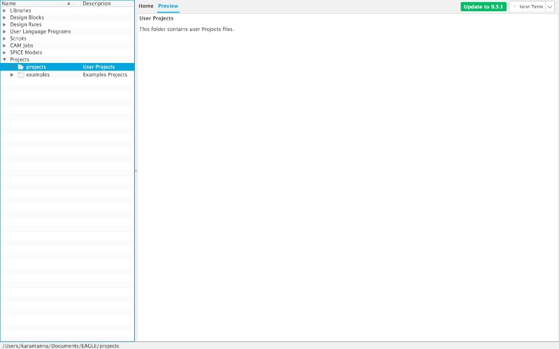
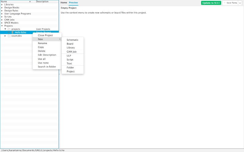
Step 1: Open Eagle. Create New Project.
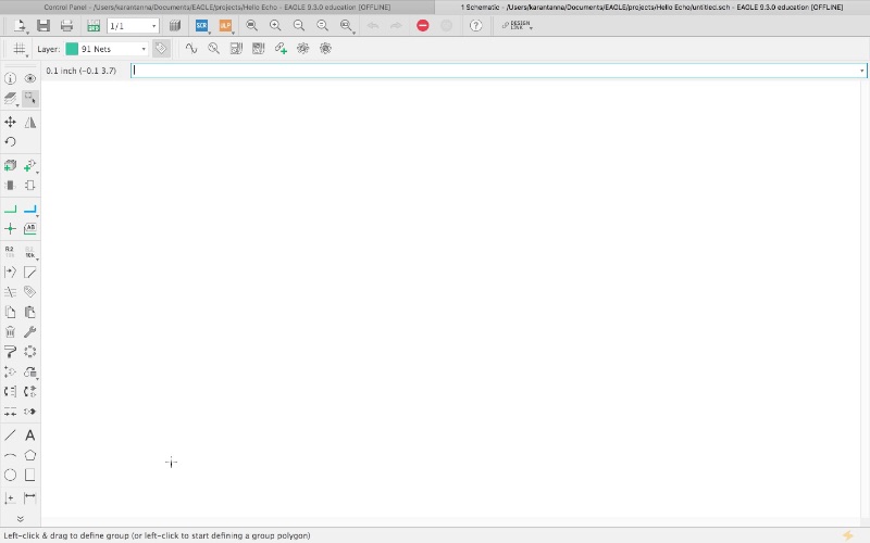
Step 2: Create New Schematic.
The eagle window looks like below.
Step 3 : Add Library. Go to Library Manager.
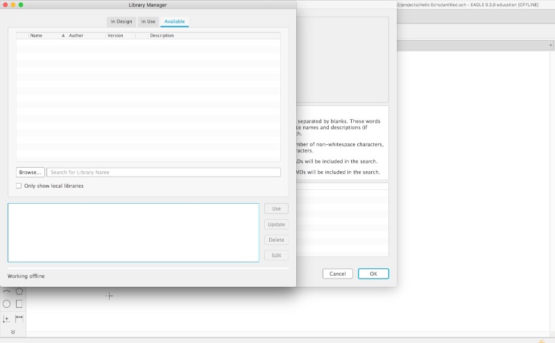
Step 4: Browse. I have already downloaded fab library. So I will just browse it. You can download it from below.
Note: The simple stratagy I used to place parts was to place them modularly according to circuit, meaning ideally it should be placed at minimum distance from the corresponding parts.
ie. Crystal/Resonator near to XTAL pins. It also gets easier to route.
Usually in board layouts, the components are laid out in a vertical and horizontal manner (not in angle).
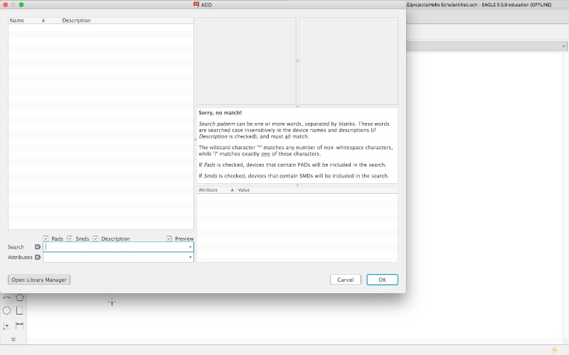
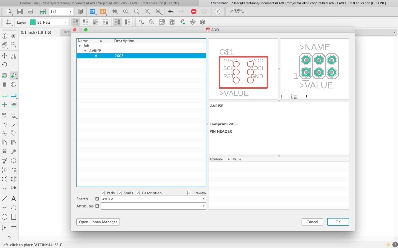
After Adding Library, Add all required parts.
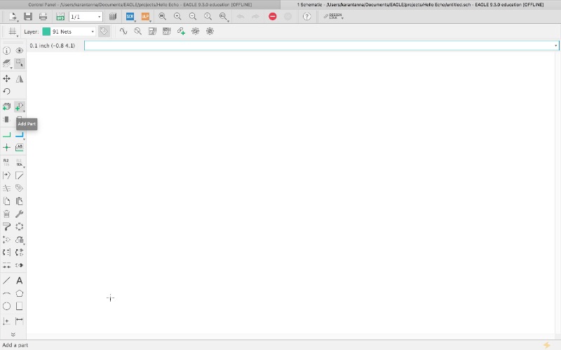
Use add part tool to add parts.
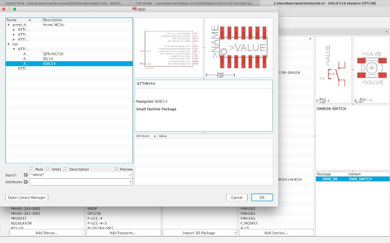
Select part that you want. Add them one by one.
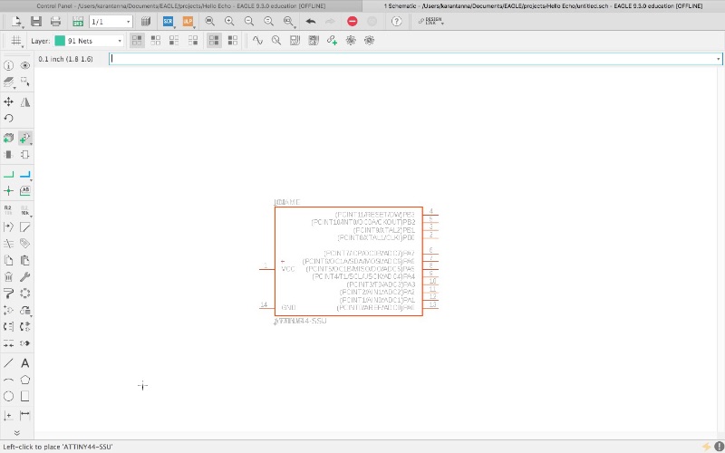
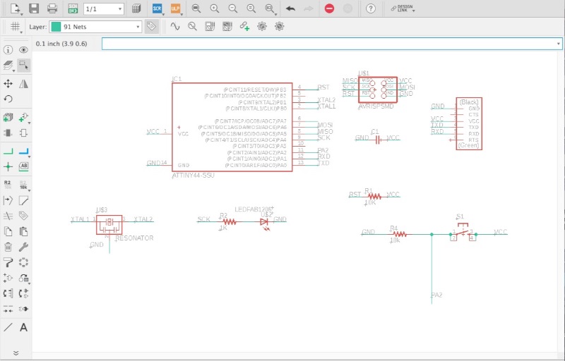
Step 5: Similarly add all other parts. It will look like below
Note : Name all the parts using 'name' command. Also put Value to each part using 'value' command. It gets easier to locate parts and also you won't get ERC errors due to these.
Step 6: Using Net command connect parts as below.(You can give same name and it will connect automatically. For that extend nets from parts and name the net using 'name' commad.
Check ERC. (Refer ERC section at the later part of page.)
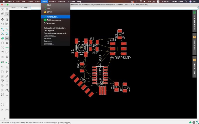
Step 7: Then Switch to Board Mode. ( I re-arranged it to route it.)
In case if you get errors while using Net-connections, or if you make mistake. It is better to delete all nets and reassign it. Otherwise board may not work. (Worse is if you interchange or short VCC and Ground.) You can check when you connect it and it doesn't show correct connection.
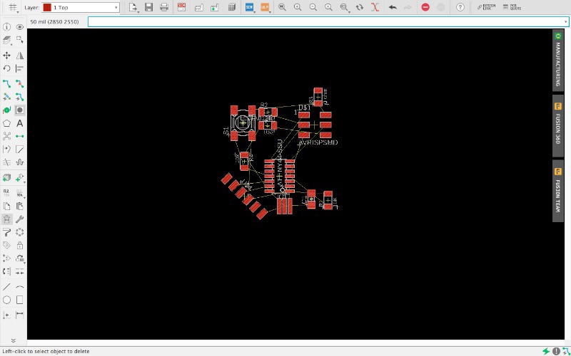
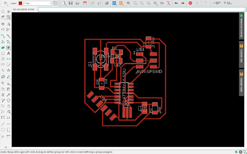
Step 8: You can use auto router to route. This method involves lot of trial and error. Its always good to do manually. I routed it as below.
Note: Incase if you get errors in routing, then you can do manually by following the Rat-Nets. Also you can know if any route is missing by Rat-Nets.
Note : As I had closed loops/incomplete routes, (I had no way out to make connection as the other traces were intersecting.)
I used 0 ohm resistor as jumper.(It connects the two traces without inter-section.) I used 16 mill thickness for routing which its good thickness. You can go upto 10 in certain cases. Smaller than that traces might come out while milling.
Check if all the Rat-nets are gone and also refer it with schematics to know that your routing is OK and you are not missing any routes.)
p>
Check DRC. (Refer DRC section at the later part of page.)
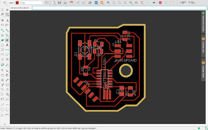
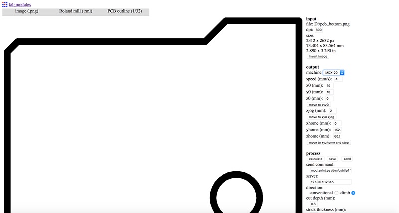
Step 9: Make outline in new layer (I used Dimension layer). I used 32 mill thickness for outline. (30-40 is good range.)
ERC and DRC
What is ERC?
It is Electrical Rule Check.
Syntax : ERC
This command is used to test schematics for electrical errors.
The ERC command also performs a Consistency Check between a schematic and its corresponding board, provided the board file has been loaded before starting the ERC. As a result of this check the automatic Forward&Back Annotation will be turned on or off, depending on whether the files have been found to be consistent or not.
Please note that the ERC detects inconsistencies between the implicit power and supply pins in the schematic and the actual signal connections in the board. Such inconsistencies can occur if the supply pin configuration is modified after the board has been created with the BOARD command. Since the power pins are only connected "implicitly", these changes can't always be forward annotated
. If such errors are detected, Forward&Back Annotation will still be performed, but the supply pin configuration should be checked!
What is DRC?
Checks design rules.
Syntax:
DRC
	DRC * * ;
		DRC LOAD|SAVE filename;
The command DRC checks a board against the current set of Design Rules.
Checking ERC errors
Step 1: Go to Tools > ERC.
You'll get list of errors in schematics.
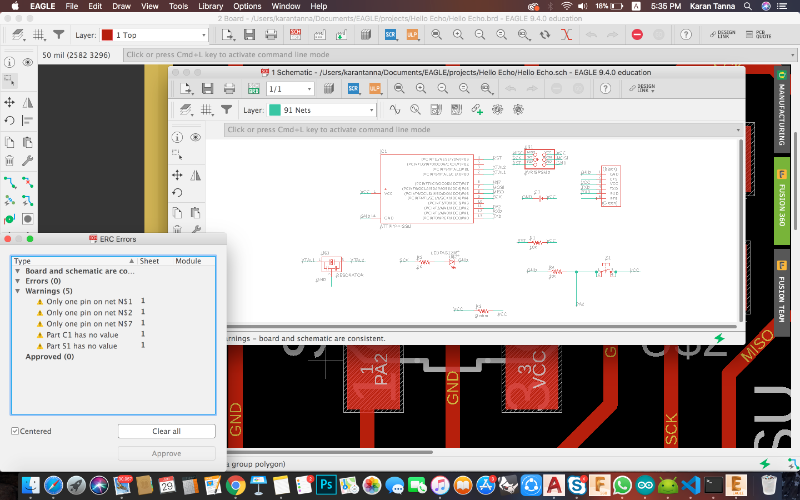
Step 2 : Check it by clicking each and correct it. Then save and perform it again.
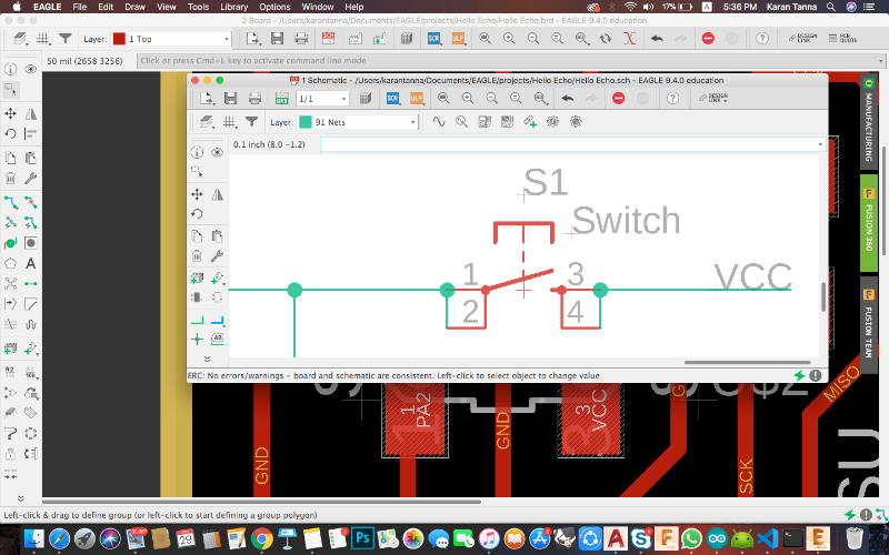
You'll get to see the above notification below schematic window. Now you're good to go for exporting and milling.
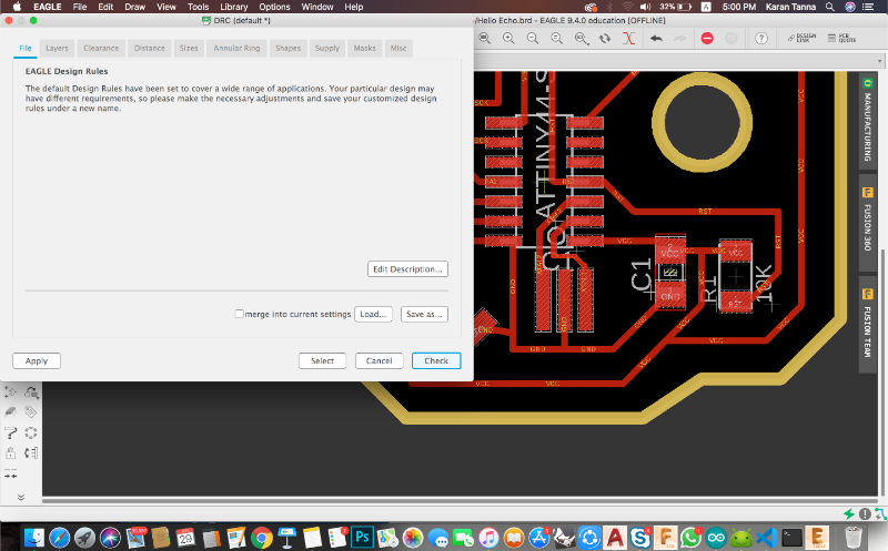
DRC Rules
We can set our DRC rules for PCB, and change it depending upon our requirement. Here I have set my DRC rules according to milling machine, ie. we performed clearance test in Week 5 group assignment. From that we found that upto 10mill milling is good.
Step 1 : Go to Tools > DRC. The box as below will open.
Step 2 : Go to Clearances.
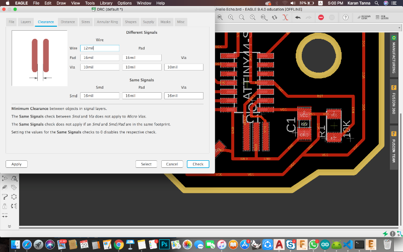
Here wire I kept as 12mil. Others are as is. We are not using vias here. Also pads are big enough.
Step 3: Then go to Sizes.
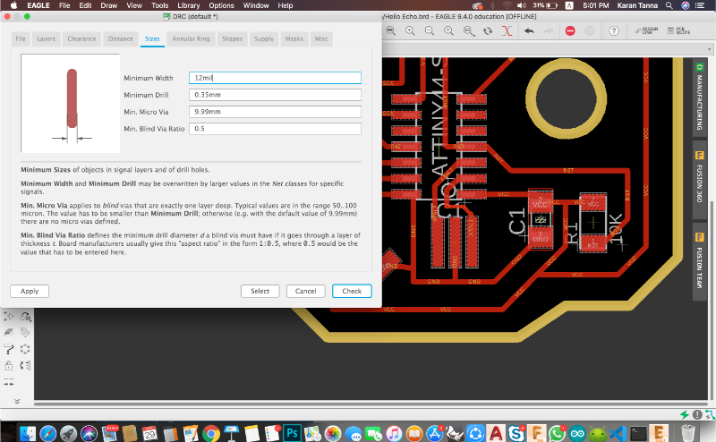
For this the minimum size was kept 10mil. We are not using drills or vias here.
Step 4 : Then apply it and check.
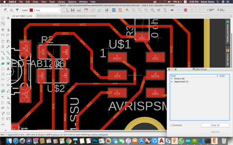
Step 5 : You'll get the list of errors. Here there is one error. But that wrror is due to jump resistor. We can make exception for such errors as both terminals are named same. Thus approve it.
Exporting PNGs using Script.
Step 10: Go to File> Execute Script. Browse annd Run it. You'll get PNG files in given folder.
Note: You cam export it manualy using File>Export>Image.
For Traces, you need only Top Layer. Hide other layers.
For Outline, you need the layer in which you drew outline. (In my case Dimension layer.)
You can decide the resolution of the image as well. (1000dpi-1200dpi is good.)
The above script Hides all the non-required layers, and exports images one by one with said resolution.
Step 11 : Mill and Solder it. To Know how to do that go to Week 5.
PNG Files
Using the Module
Go to fabmodules.org
In terminal go to directory and write "npm start" or "sudo npm start"
It will prompt you that it is getting data from server.
Note : You need to invert PNG of traces in the mods/modules.
I used following parameters to mill the board.
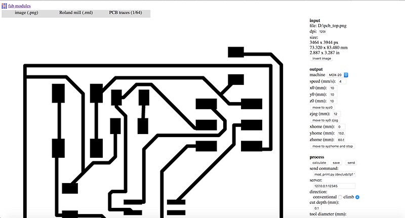
Invert image while milling tracs.
Important Parameter Table : Traces - Machine MDX-20
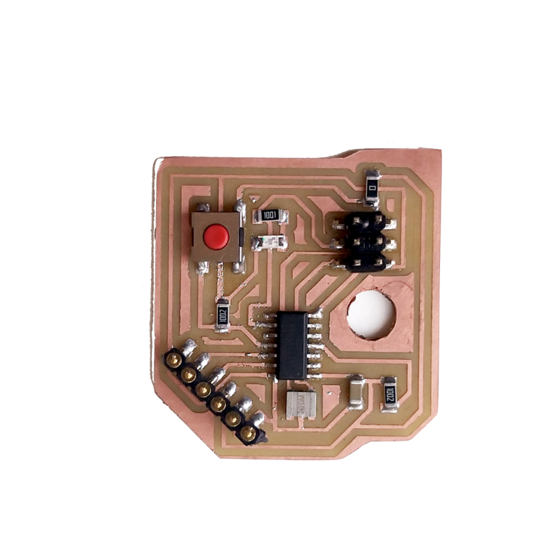
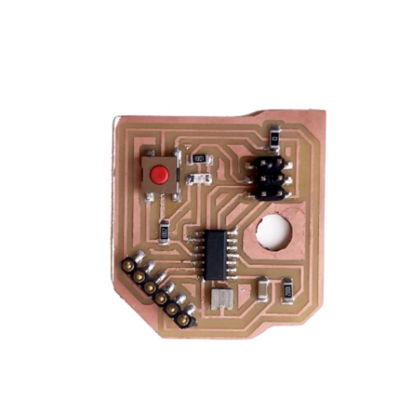
Soldered Board
The soldered board would look like below.
Blink Test
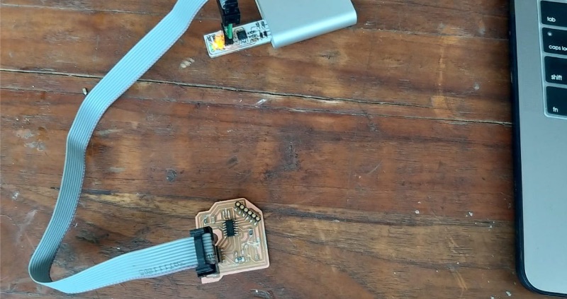
Step 1 : Connect board to FabISP using 6 Pin Headers (Follow ISP Pinout)
Step 2 : Open Arduino IDE to program the board. You can Download Arduino IDE using button below.
Step 3: Then go to tools and assign respective parameters : 1. Board 2. Port 3. Programmer
Step 4 : Write Code. Code I used is as below.(Note : Just re-check the pinns that you are assigning.)
	void setup() {
		// initialize digital pin LED_BUILTIN as an output.
		pinMode(LED_BUILTIN, OUTPUT);
	  }

	  // the loop function runs over and over again forever
	  void loop() {
		digitalWrite(LED_BUILTIN, HIGH);
		// turn the LED on (HIGH is the voltage level)
		delay(1000);
		// wait for a second
		digitalWrite(LED_BUILTIN, LOW);
		// turn the LED off by making the voltage LOW
		delay(1000);
		 // wait for a second
	  }
Step 5 : Upload Sketch and See it blinking when you press button.(set values according to you)
(This week I tried Embeded Programming with this. I have explained code in Embeded Programming Week.)
What Did I learn ?
This week I tried to understannd Circuit and Schematics.
I researched and learned about laws of electronics and key rules to design circuit.
Since I never used Eagle CAD before, I started to understand workflow of same.
While arranging components in Eagle CAD, I figured that it is easy to route when components are arranged according to modules of schematics.
As I wasn't able to route due to a closed loop, I solved it with 0 ohm resistor and jump over the trace.