5. Electronics production
Assignment
This week we had two assignments. The first was our group project which required us to characterize the design rules for our PCB production, and the second was to make an in circuit programmer by milling the pcb and programming it.
Group Work
We began the group portion of this assignment by sitting down with our milling machines and trying to cut out the provided test file that Neil mentioned in class.
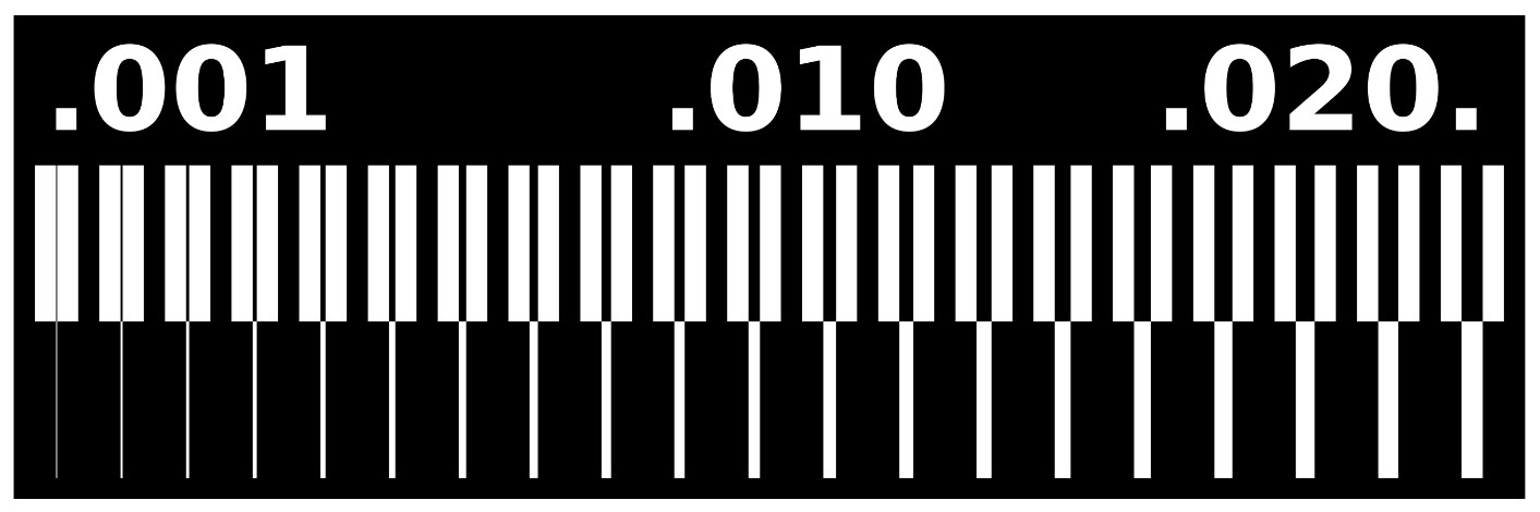
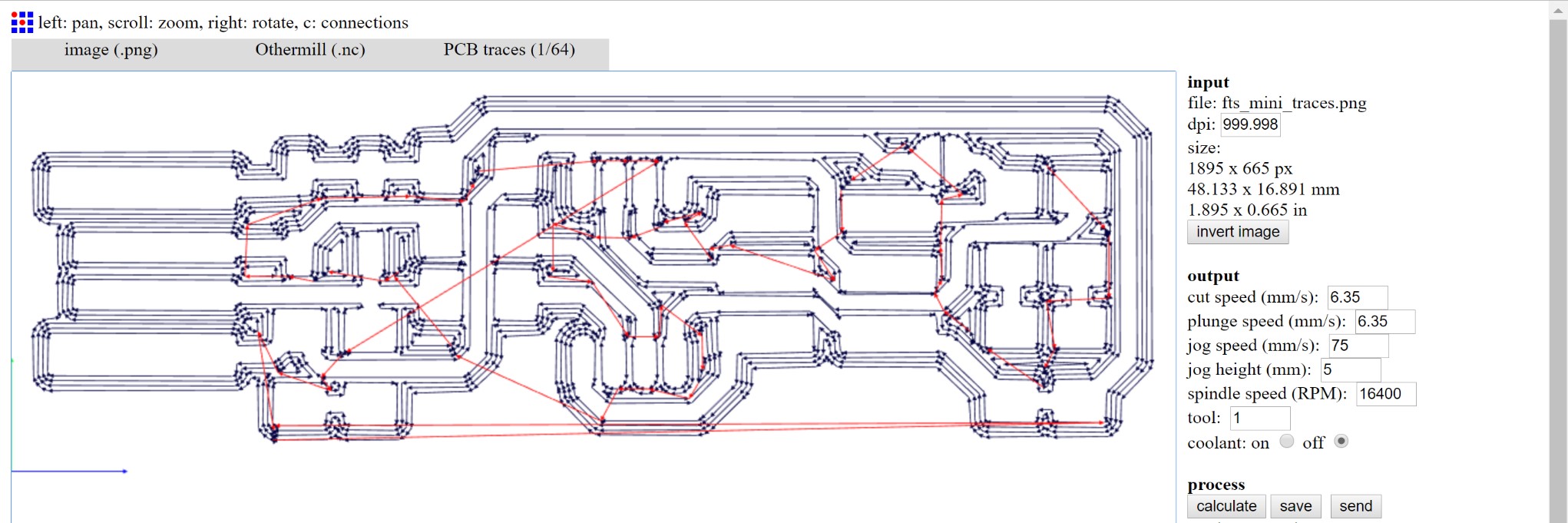
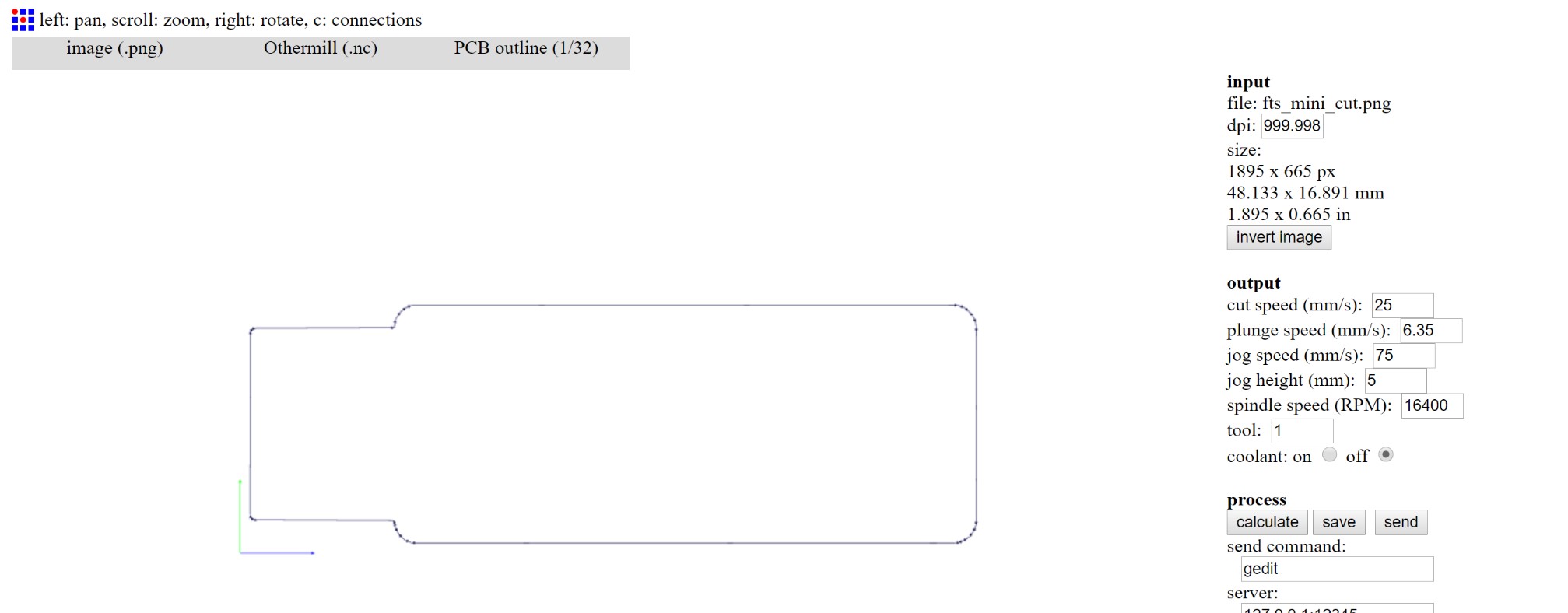
To help us get going, we looked through a few sites from previous students. We found that Mary Fabian from the lab at Charlotte Latin had used a site called Fab Modules last year to get her files ready for the milling machine, so we chose to do the same. We first started by saving the test cut file that Neil showed us on the computer as a PNG. Then, we opened up Fab Modules, imported the PNG, selected the type of file we would need out which was labeled as Othermill (.nc) for the Othermill Pro machine we were using, and lastly we chose the type of cut we were doing, which was pcb traces with a 1/64th inch bit size. After selecting everything as needed, we then hit calculate, let the program do its thing, and saved the trace file onto the computer. This is what the trace file for the test cut ended up looking like in Fab Modules.
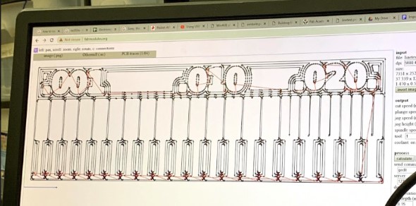
Next, after the file was ready for the milling machine software, we opened up Bantam Tools to communicate directly with our Othermill pro milling machine. We imported the file into Bantam, checked to be sure the bit size was correct, made sure that the x, y, and z axes were all properly homed, then we got the material itself set up on the machine.
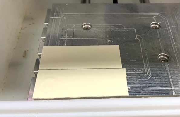
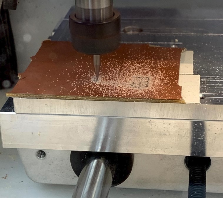
We used basic one sided pcb material for this test cut that measured 1.54 mm in thickness. To hold the pcb down onto the cutting bed, we used a special type of super strong double sided tape that doesn’t leave behind any sort of residue, then we were sure not to let any of the tape overlap because that would cause leveling issues with our cut. The picture above shows the tape and the one below shows the PCB firmly secured to the cutting bed.

After things were ready on both the software and physical side of things, all we had left to do was run the cut.
After running the cut we realized we would need to do a second, deeper cut to separate our traces from the whole piece of stock pcb board.
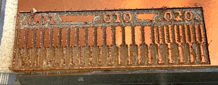
We found the outline cut file, went through the same process as before of getting it set up in Fab Modules as well as in Bantam Tools, then once that was all ready we switched the bit out for a 1/32nd inch sized bit to do the outline cut with. When we switched the bit out, we also had to re-home the Z axis. Once everything was set, we ran the second cut to separate all of our traces. This is what we were left with.
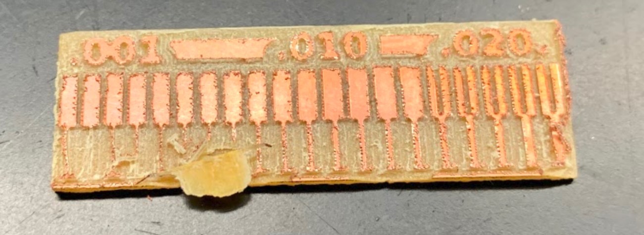
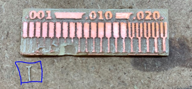
The test cut came out a little rough, but we used sandpaper to do a bit of post processing and clean it up some more. As you can see, though, the sandpaper accidentally pulled one of the trace lines off with it.
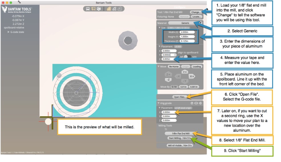
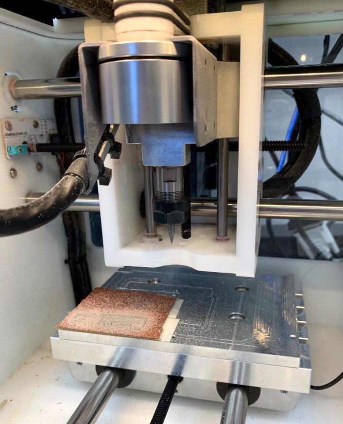
The test cut was effective in getting us used to the machine process as well as in letting us know what our machine is capable of. Below is another helpful graphic we used to familiarize ourselves with the setup process in bantam tools.
Individual Assignment
My individual assignment this week was to make an in circuit programmer by milling out the PCB and programming it. On the day that we did our group assignment, we also ran a couple of cuts for the programmers themselves so that we could go ahead and start practicing the soldering. I did manage to assemble a working programmer that day, but I wasn’t actually the one that cut out the PCB so I couldn’t count it as my own work. Regardless, though, it was good practice for surface mount soldering so I will include photos of that.
I managed to fully make my own pcb as well, which I will detail below.
Milling the Board
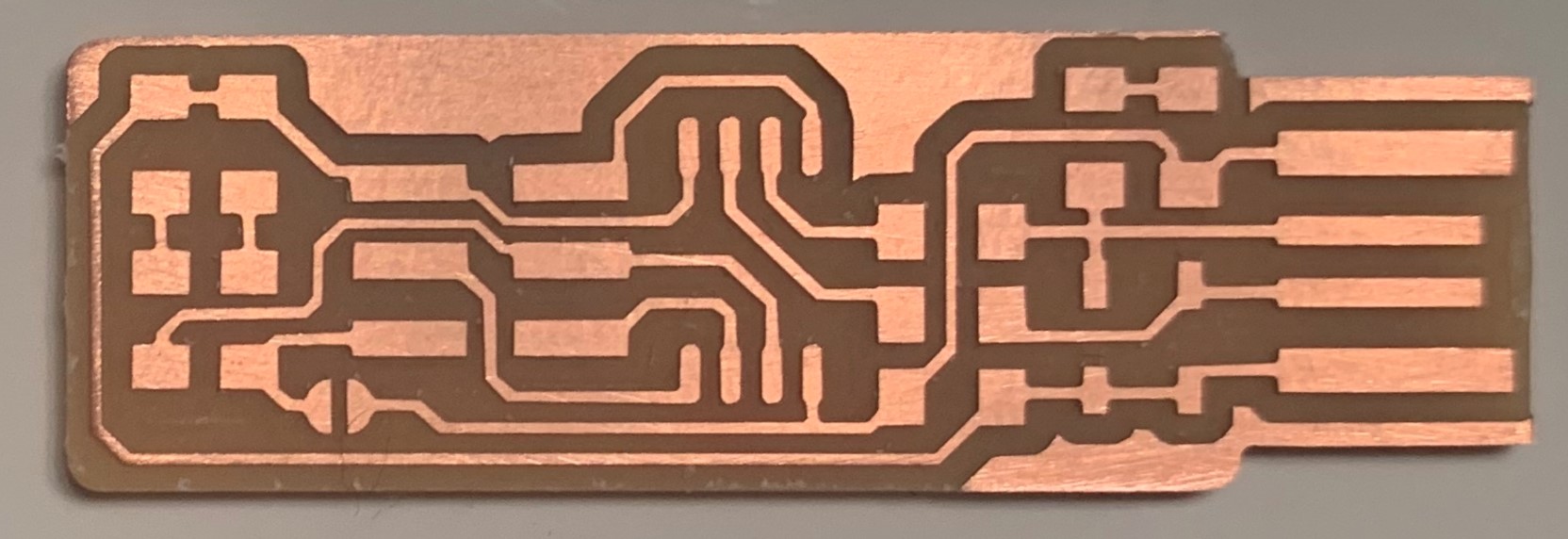
I started with Brian’s tutorial on how to make the PCB as suggested by my lab instructors. I grabbed the trace and outline cut files from there, saved them both as a PNG on my computer, and loaded them each up into Fab Modules.
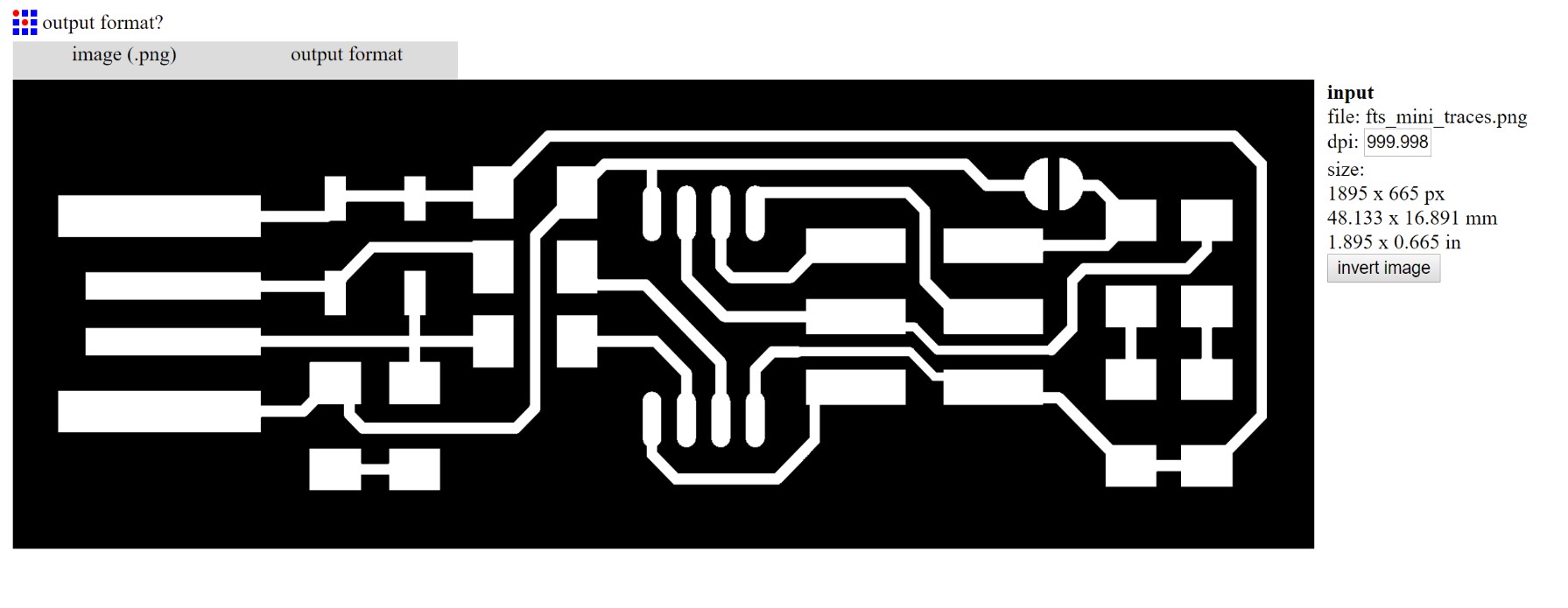
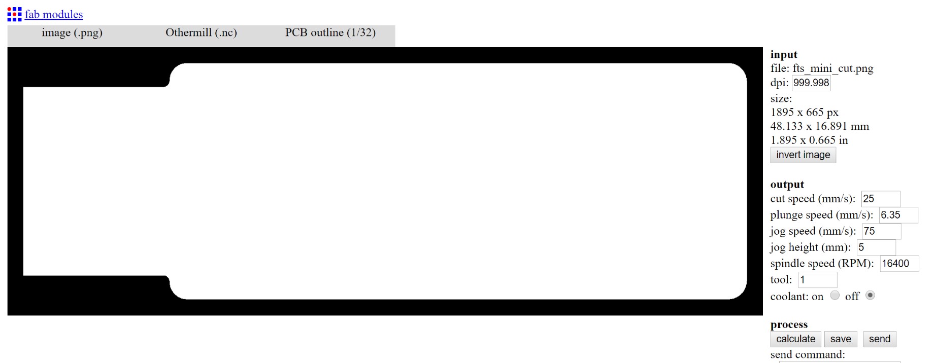
After getting them each put into Fab Modules, I selected the necessary file type and tool size for each, 1/64th for the traces and 1/32nd for the outline, and then I hit calculate and let the program do its thing. This is what I got for each after calculating.
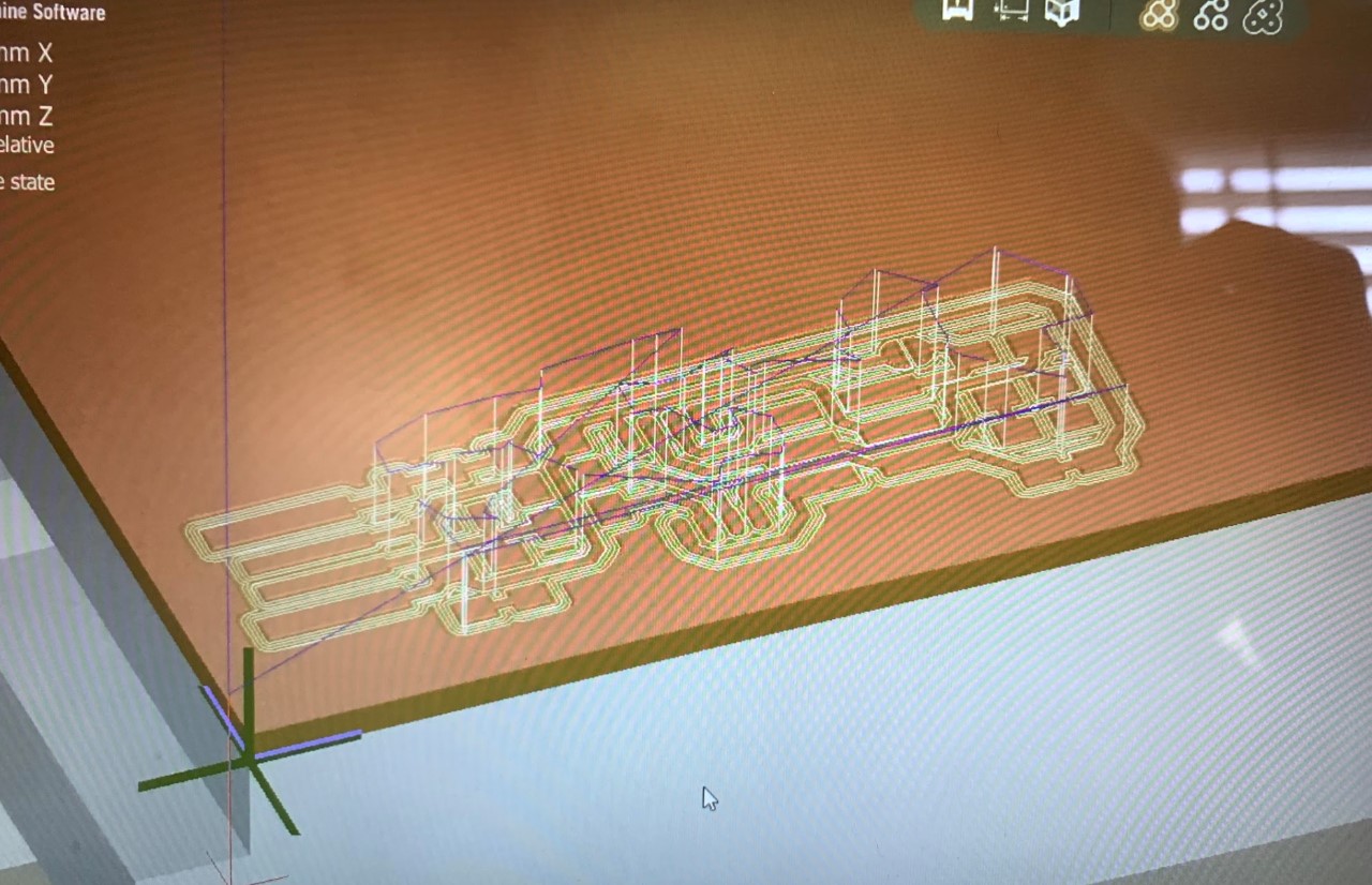
Next I had to import each file over into the Bantam tools software. Once the files are in Bantam, you can easily see how the cut will look as well as how the trace pattern itself looks too.
Then, after getting the files brought over, I measured the thickness of the PCB as well as the thickness of the tape it sits on, added those together, and input that into the software for the material thickness value. After setting the thickness, I homed the X and Y axis to make sure everything was right, then I got a 1/64th inch bit for the trace cuts and switched out the bit.
After switching the bit, It then prompted me to locate the tool in the software by homing the z axis. I checked to be sure it wasn’t going to measure off of the tape, then I hit locate and it homed the Z axis.
Everything was ready at that point, so I removed the second side of the adhesive cover on the tape, placed down my PCB securely, closed up all the windows of the machine, and ran the cut.
About halfway through, the machine finished up the trace cut with the 1/64th inch bit and prompted me to switch the bit to a 1/32nd inch size so that it could then do the outline cut. It conveniently brings the head to the center of the machine for you which makes it super easy to swap in a new bit.
After swapping in the new bit and closing up the door once again, the machine automatically resumed and finished up the outline cut.
After the cut was done, I used our labs shop vac to clear the dust and other particulate out of the machine, then I carefully pried the board away from the cut bed with a hard flat edge.
At this point the board was all finished up, I used a bit of fine sandpaper to remove some of the burrs around the edges and then It was ready to be soldered.
Soldering
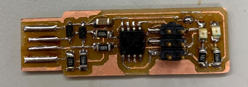
Over the course of this week I actually ended up soldering three separate boards. The first two were more for practice than anything else, and the third was my final result. I have already included pictures of the first board above, but here are some more pictures showing the second practice board I made.
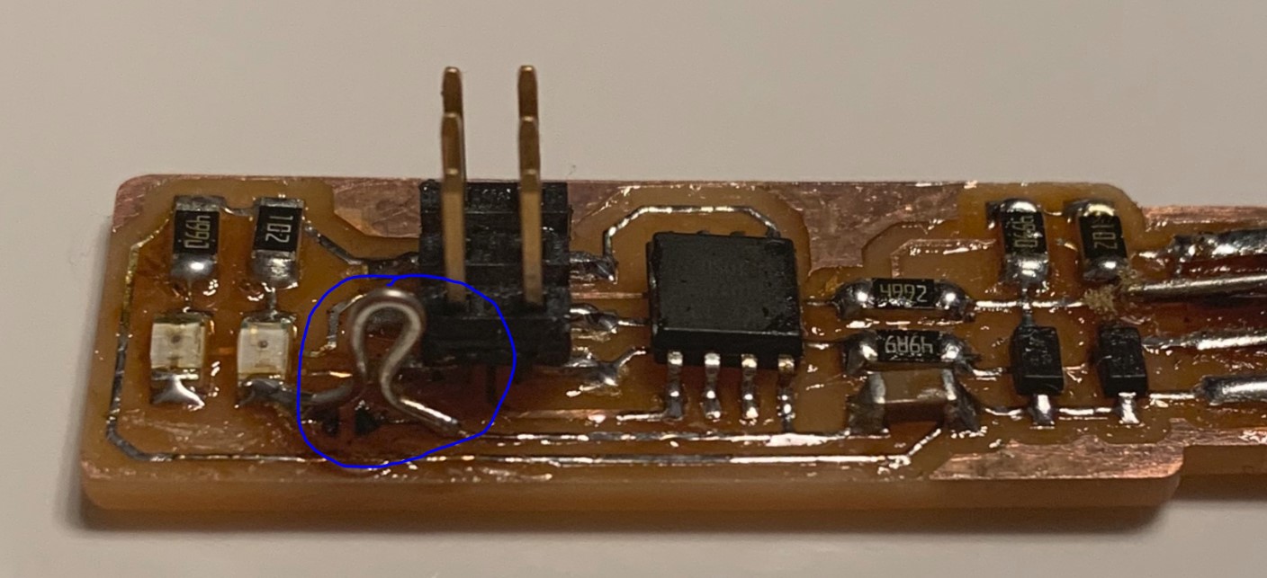
As you can see, I actually ended up doing worse on the second one because I wasn’t able to get the jumper connection soldered correctly and a few of the traces lifted up when I was trying to solder the USB connections. To try and resolve these issues, I attached a usb header to the broken trace line as well as to the other trace lines which holds the broken trace down fairly securely, and I used a small piece of wire to fix the jumper connection. For some reason when I was soldering, the solder on the two separate pads of the jumper didn’t want to join and make one uniform connection, and while I was continuing to try to make it work the heat from the soldering iron caused one of the traces to lift and break. I did manage to fix this, though.
Surface mount soldering can be pretty tough, plus I hadn’t done much it before this week, so that meant there was a lot of new info for me to learn. One thing in particular that I had never worked with before was the concept of using additional flux.
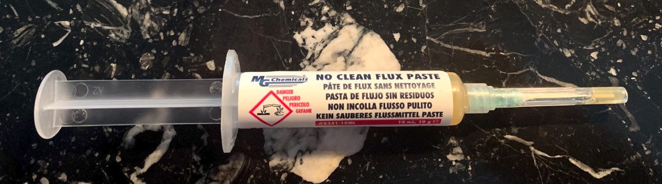
With through hole soldering, you generally don’t need to worry about the flux too much because it’s actually inside of the solder wire we all use. However, having the flux in the wire itself only really works when you melt the wire directly onto the joint. If you want to get some solder on the tip of your iron, then bring that solder over to the joint to apply directly, then by the time you bring the iron over all of the flux from the wire will have burned off by then. To solve this problem, there is a product called flux paste that you can apply onto the joints before soldering. The flux paste helps the solder flow consistently and it comes in an easy to use syringe, pictured below.
I got started by using double sided tape to secure my board to the top of a piece of tile. This keeps the board stable during soldering and it also makes it really easy to turn the board to any position that you need to get the best angle for surface mount soldering.
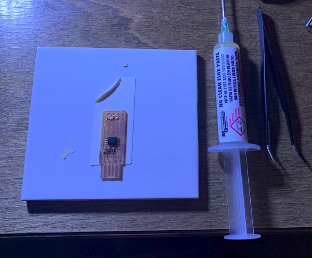
As you can see from the picture above, I actually went ahead and started soldering before I remembered to get a pic of the board being taped down.
Surface mount soldering was tough to get the hang of, but by my third board I was pretty used to it. The thing with surface mount soldering is that you actually need three hands to do it well. One for holding the soldering iron, one for holding the solder itself, and one for holding and placing down all of the teeny tiny parts. Fortunately for us humans though, there are methods that don’t require quite as many appendages. For example, you can actually put down some solder on the pad that you want to make a connection with before you even pick up the part itself. This way you eliminate the need for your third hand that comes in and holds the soldering wire because the solder is already there, all you have to do now is touch the solder with your iron to re-melt it and then slide in the part you want to place. This is great because it forms a good connection joint between your part and the board all while firmly holding the piece in place for the other side to be soldered.
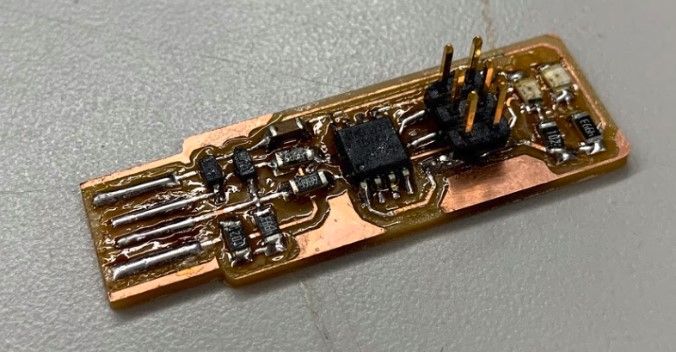
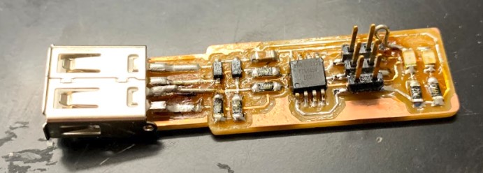
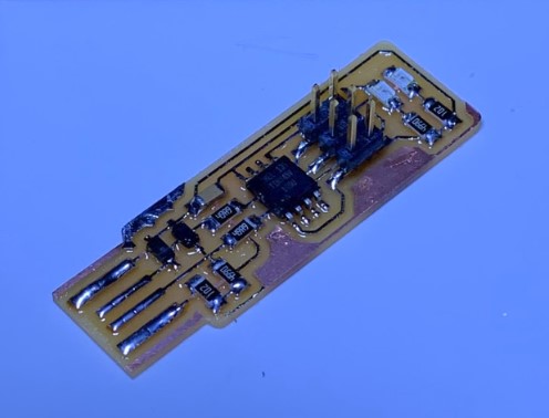
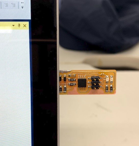
I got each part put on, keeping in mind the polarity of the diodes and leds, and this is how my finished result came out.
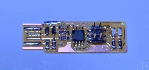
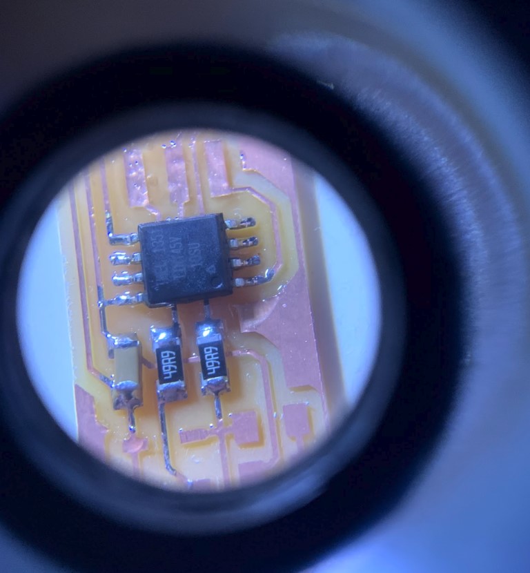
After finishing the soldering, I then used a focus lense to magnify the board and check that each joint was soldered correctly. Nothing ruins a good time like having a cold-solder joint in your project that you didn’t even know was there.
Programming
At this point, I had my board cut and soldered, so all that was left to do was program it.
I’ve never delved much into the world of computers myself, but I have done some basic surface level things with them such as simple code, light patterns, and other things like that. All of that previous work was nothing compared to this, though.
I started by following a guide that was set up with the help of one of my classmates,a few of my instructors, and a man named Dr. Adam Harris. This guide is essentially an updated and cleaned up version of the programming portion of Brian’s guide from earlier.
The first step was to download and install all of the corect software. I already had Atmel Studio 7, So I didn’t have to worry about that, but I did have to install “Make” for windows as well as “Avrdude”. After downloading both of these, I checked to be sure that they were installed in the correct paths, which they were, then I opened up the system properties which had the environment variable editor in it.
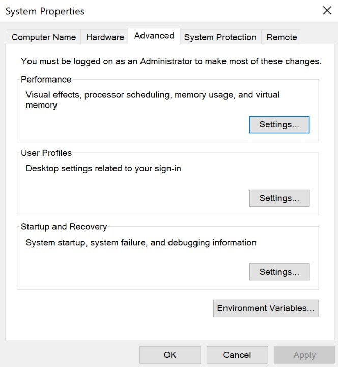
I navigated to the environment variable editor.
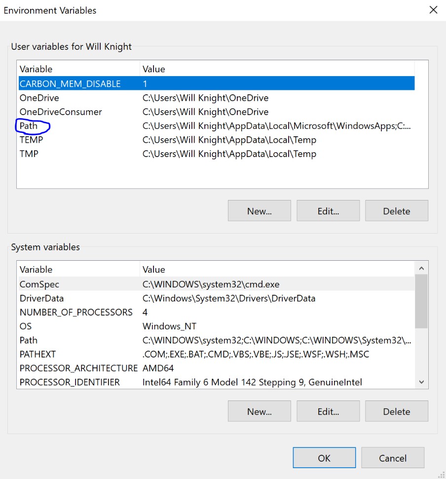
I selected the “Path” user variable, then clicked edit.
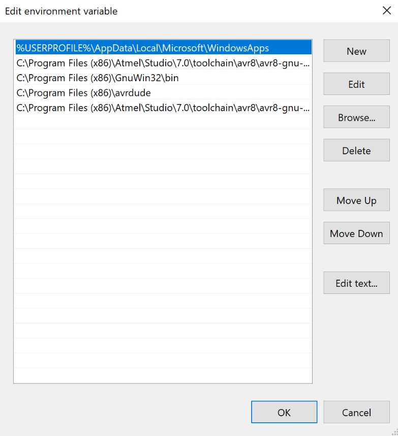
Then, lastly, I pasted in the correct paths for these new things that I had installed so that I could find them easily using the command line later.
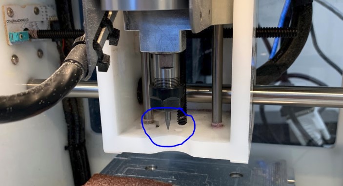
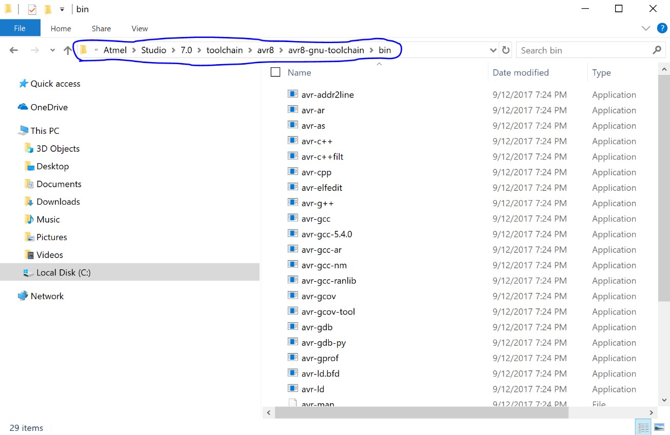
Once the paths were all installed, I went over to the command line and tested each one to see that I would get the expected response. The first two commands, “avrdude” and “make”, both worked as expected and spit back the correct responses, but when I tried the path for “avr-gcc” I kept on getting a response telling me that this was not a recognized command. To solve this, I actually had to go in through my files and find the right thing that way which took a bit of digging. After I found it though, all I had to do was copy the address and paste it in as the correct path. The address is circled in blue.
After pasting this in correctly, I checked again and this time I got the expected response.
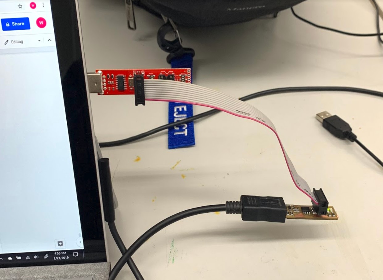
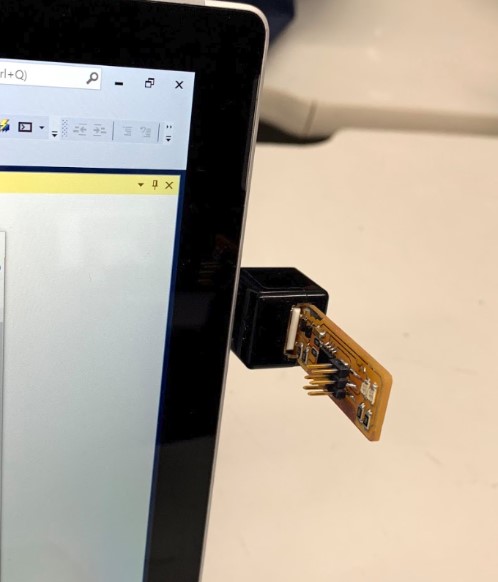
After these were set up, It was time to connect the boards. I hooked up both programmers, being sure that things were lined up correctly, then I went on to the next step.
Next, I downloaded the FabTinyISP firmware to my desktop, which was pretty simple, and unzipped it. After viewing the folder, I copied the path from the address bar and entered it into Powershell, which is essentially just an updated version of the command line with some more optimization that I found out about near the latter end of this week.
I pasted it in and then typed “dir” after to show me the directory.
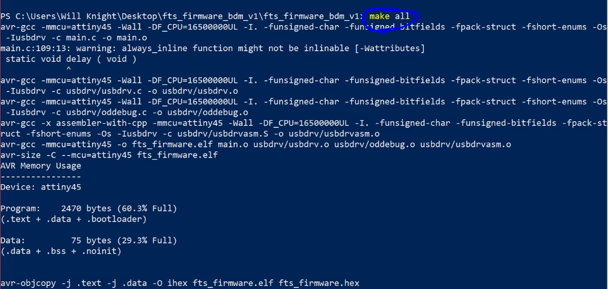
Then, I entered in “make all”, which was one of the commands I set up earlier, and it began to put together some things for me.
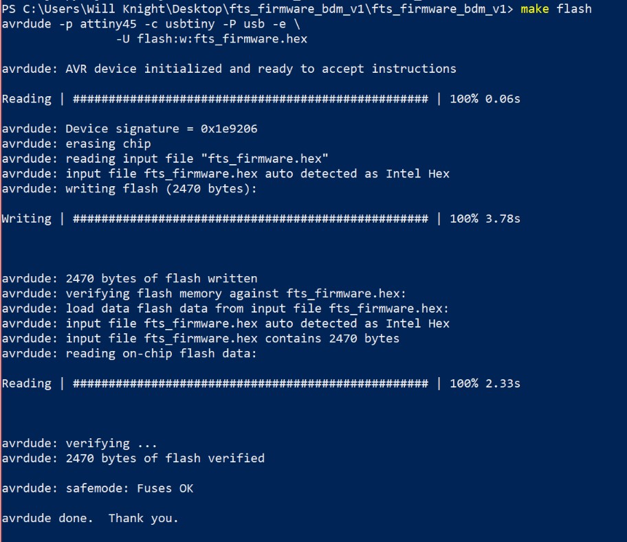
Next I did “make flash”.
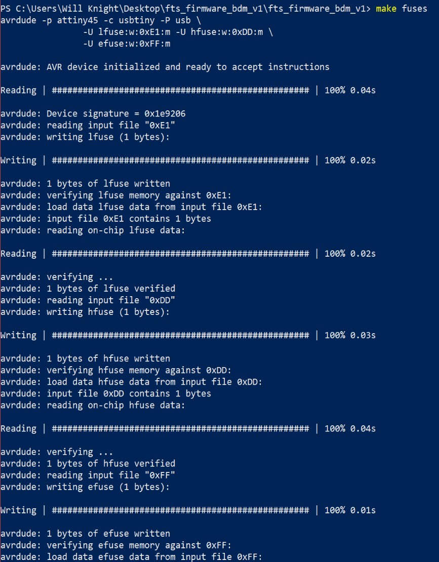
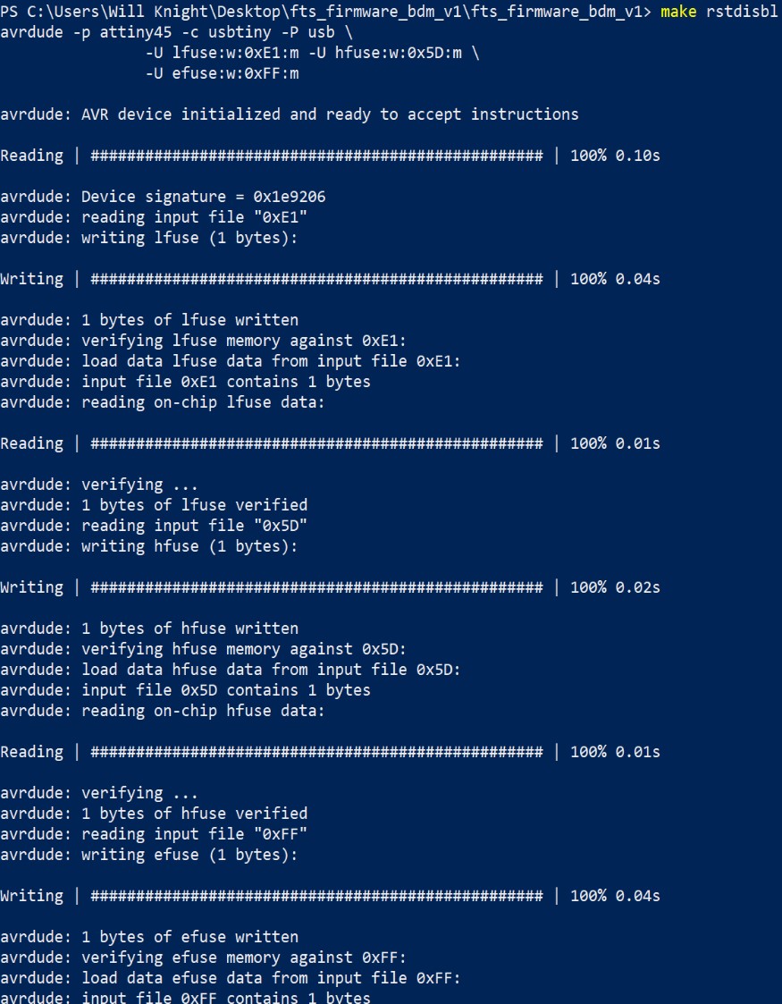
Then, lastly, I entered “make fuses”. This spit out quite a bunch of code at me so I’ll only show the top portion.
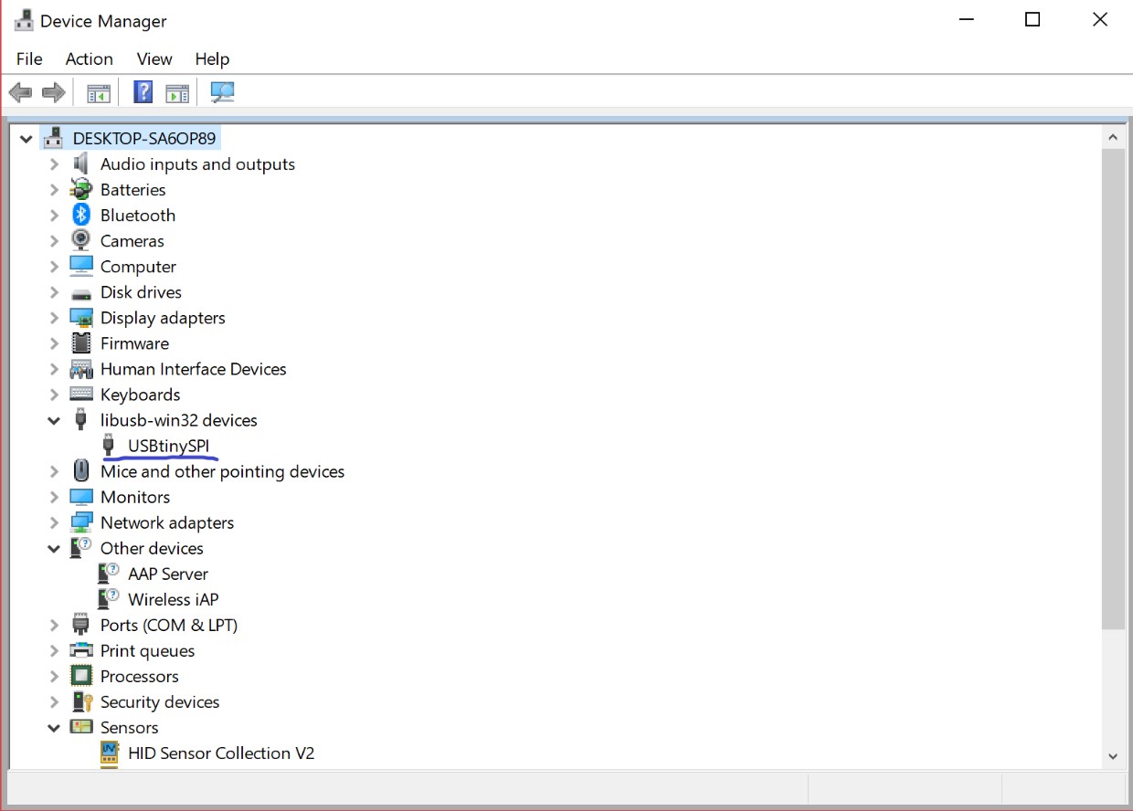
After this was done, I then had to check and be sure my board would show up in the windows device manager by itself, which it did.
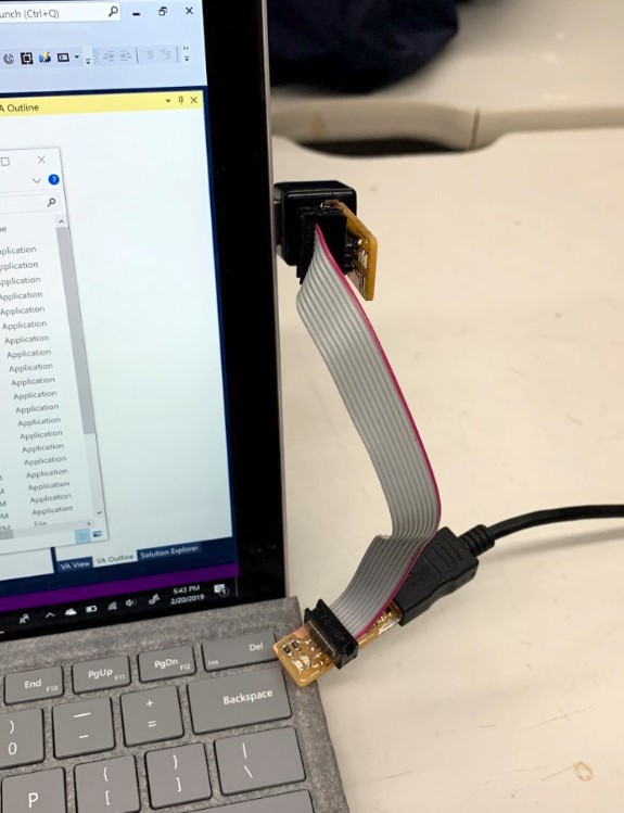
Once I saw that it was showing up in windows, I connected it back to the other programmer again and resumed the process.
Lastly, I did “make rstdisbl” which burned the last fuse. This meant that my programmer was now permanently set in being a programmer and nothing else, because that last fuse took away the ability to reprogram my board.
After my programmer was made and complete, there was only one thing left to do, programme another board using my functional one. I connected my programer up to Mr. Taylor’s board that he had just finished soldering and went through the same process as before of uploading the code and everything else. It went very smoothly and I was able to programme his board with mine, meaning that my board does officially work.
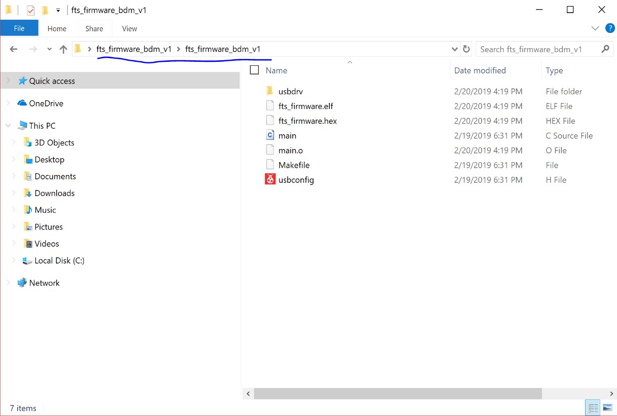
Here are all of my files from this week.