Final project / Electronics Part
Introduction
The electronics part of my project is the most important part. I decided to make wireless charging desk which has 8 charging coil on it and on master board for communication. As a base of my charging coil, I decided to peck 555 timer IC (but only at the end I realize that I can use ATtint44a as well). Desk works as a network of coils which are connected to each other by power and data ports. Master board receives data from the board and send it via Bluetooth

Wirless charging Board
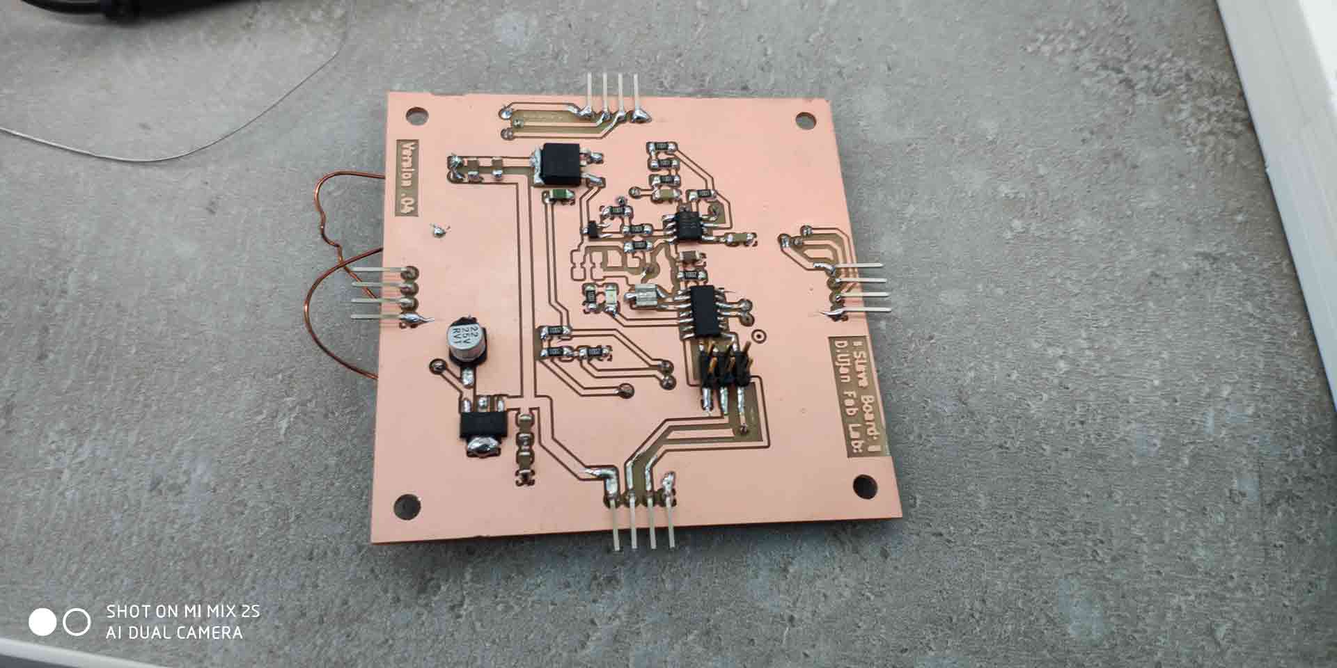
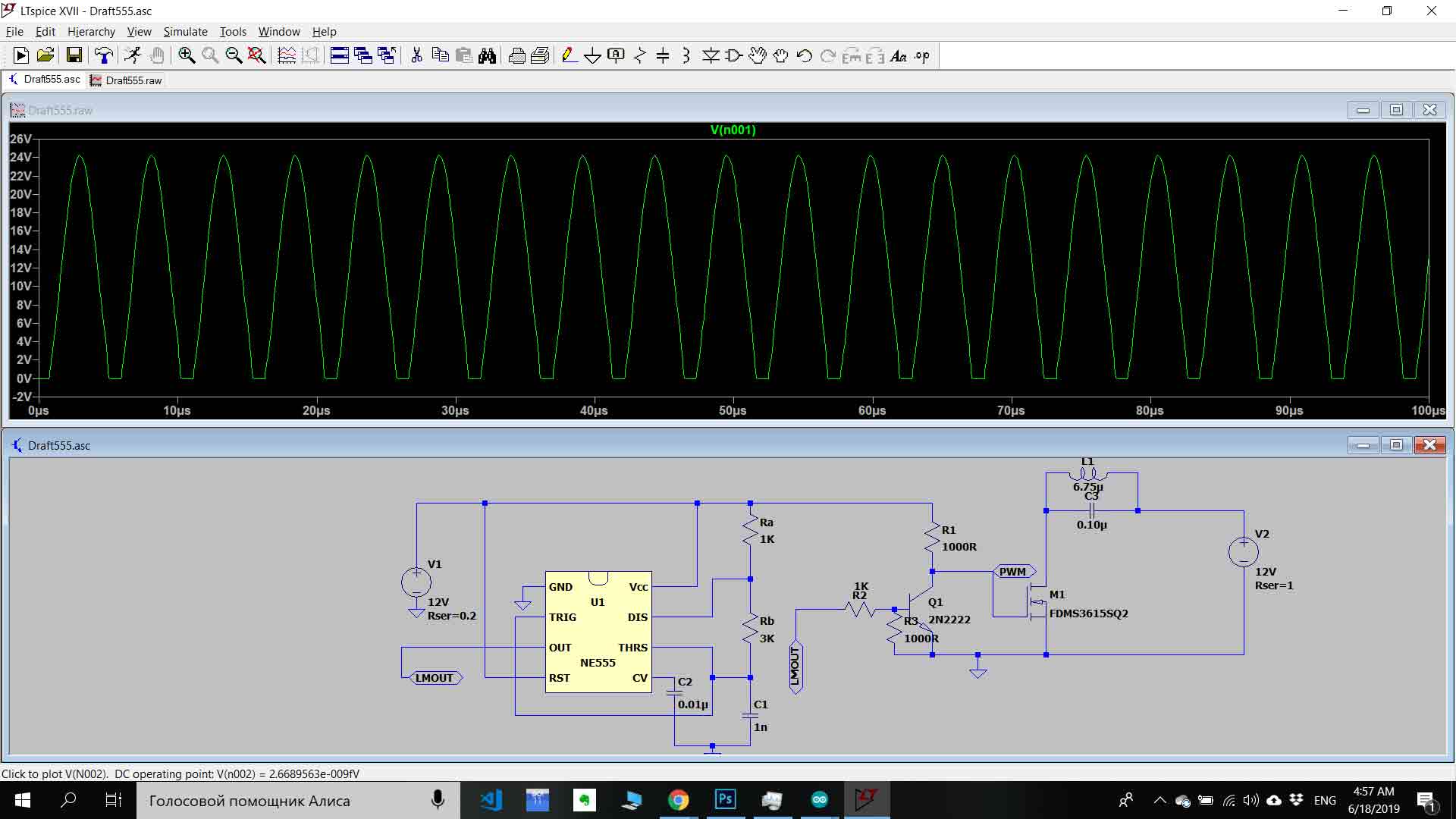
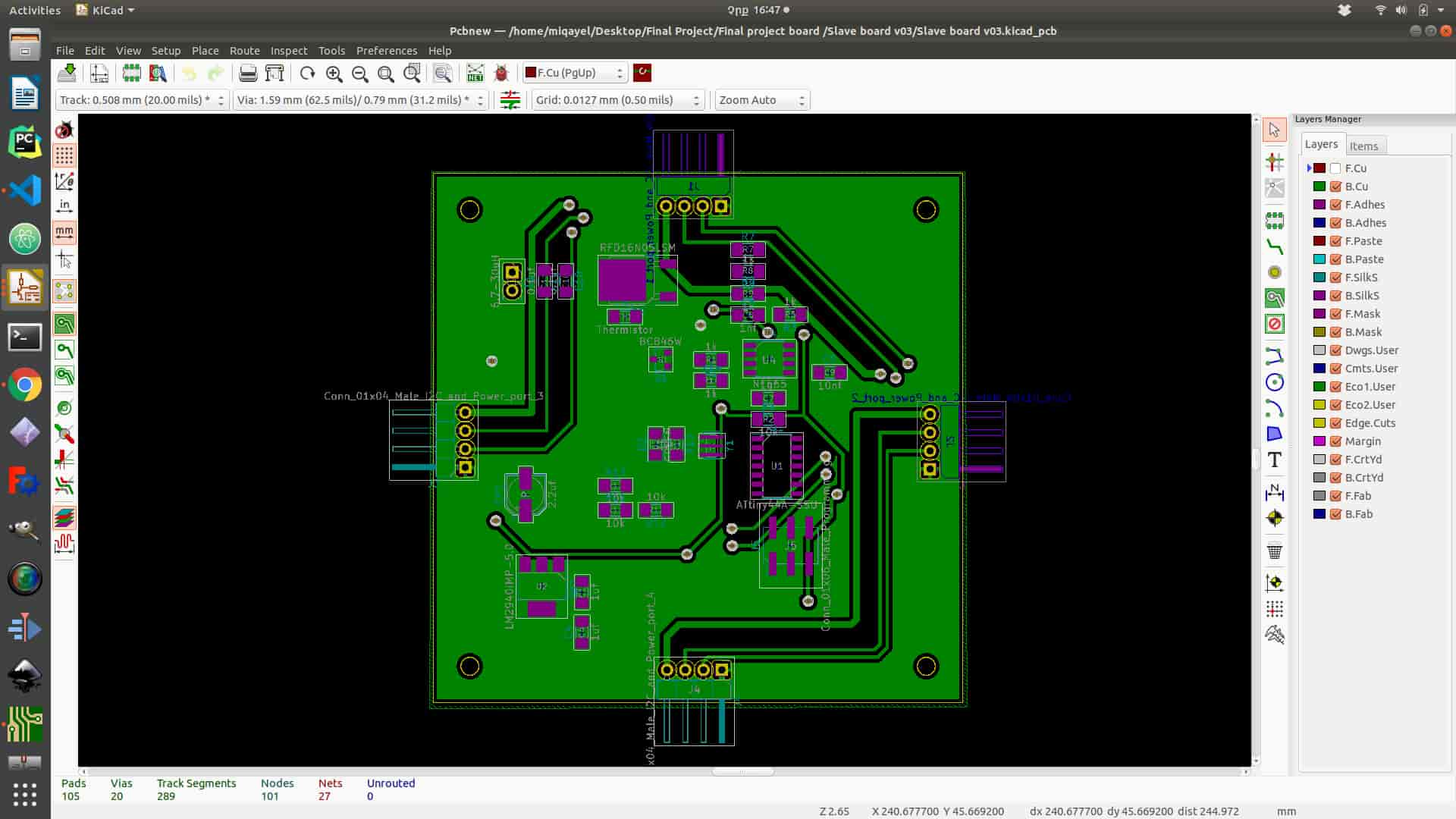
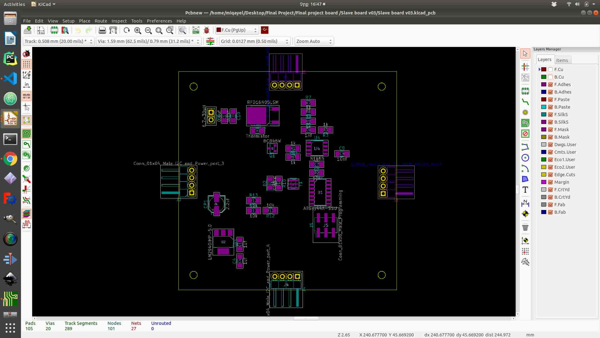
As I say in the introduction as a base of my charging board I use 555 timers also for I2C communication with a master board I used ATtiny44A-SSU microcontroller, this microcontroller is receiving temperature data from a thermistor which is nearby MOSFET transistor and send it to master board. Wireless charging Board design starts with simulations on LtSpice. I was able to simulate about 162Khz frequency (which is standard for qi charging ). After simulations, I drow schematics, understand which components I need, after getting all components I started layout design(for designing my board I used KICad software).
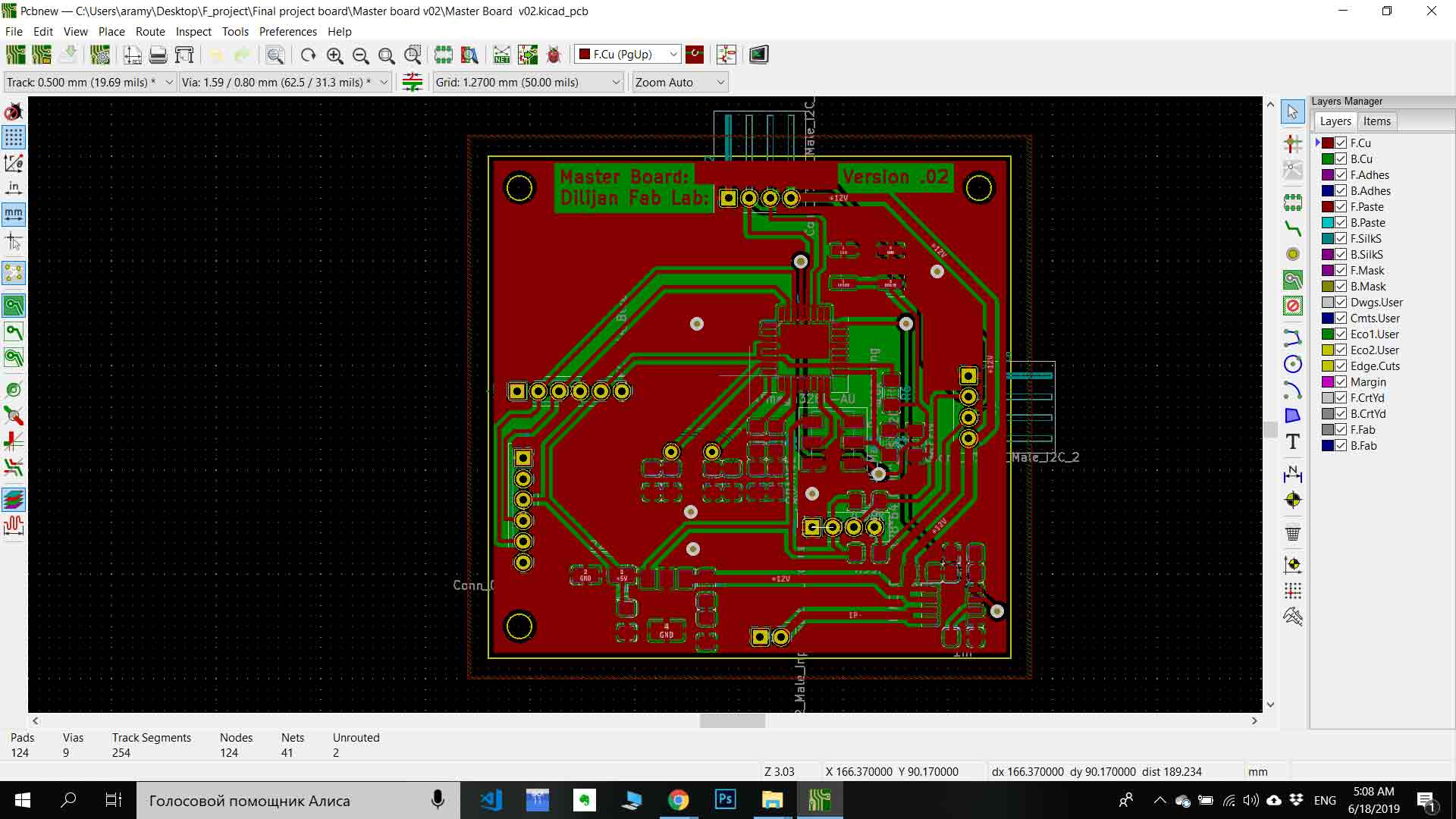
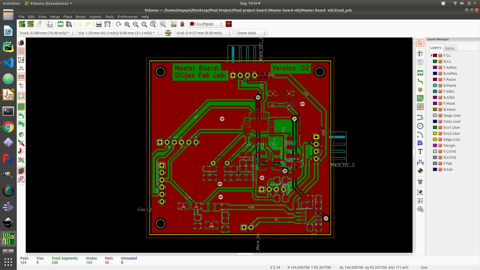
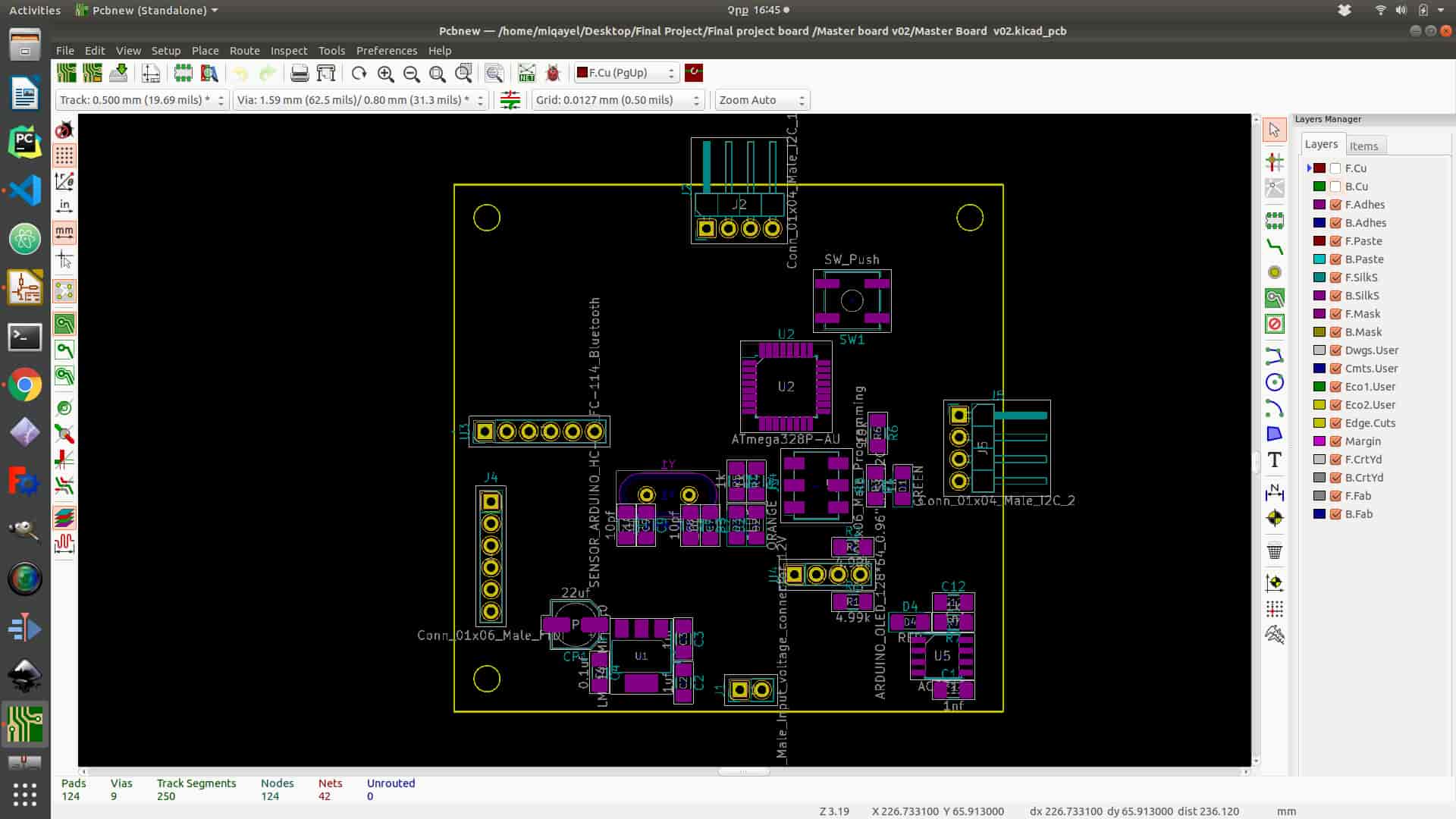
Master board
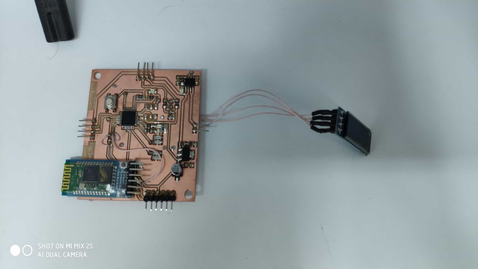
For master board I used ATmega328P-Au microcontroller which is collecting temperature data vai I2C protocol, Also It’s reades power consption from power (AC712)mesuring sensor via ADC, which is connected to power input 12V. Also microcotroller send data using HC-05 Bluetooth modul .
Board Design
Schematics
In this step, I design the actual board by choosing my board functions and components.First of all, you need to decide which components you will use(make sure you have all components), after making sure you have got everything the next step is drawing the schematics and layout of your board. After designing and double checking the board design, the next step is milling the board and soldering, and finally program and check if the board is working properly.
All components
Components for Slave board
Components for Master board
Before making blocks you need to add all components and give them value and number after that connect them (as board sample I used Neils boards). Connections are very simple all sensors I connect to PB4 and PB4 ports through switches, also as general I connect programming connector and FTDI connector to microcontroller pins. Pin connections
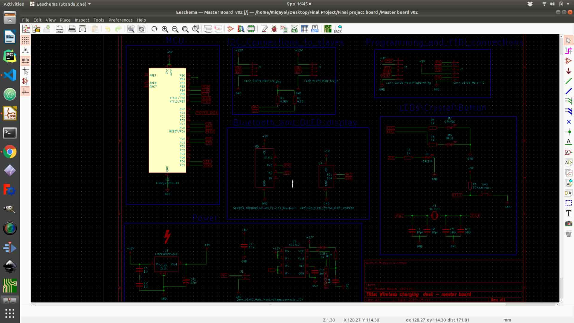
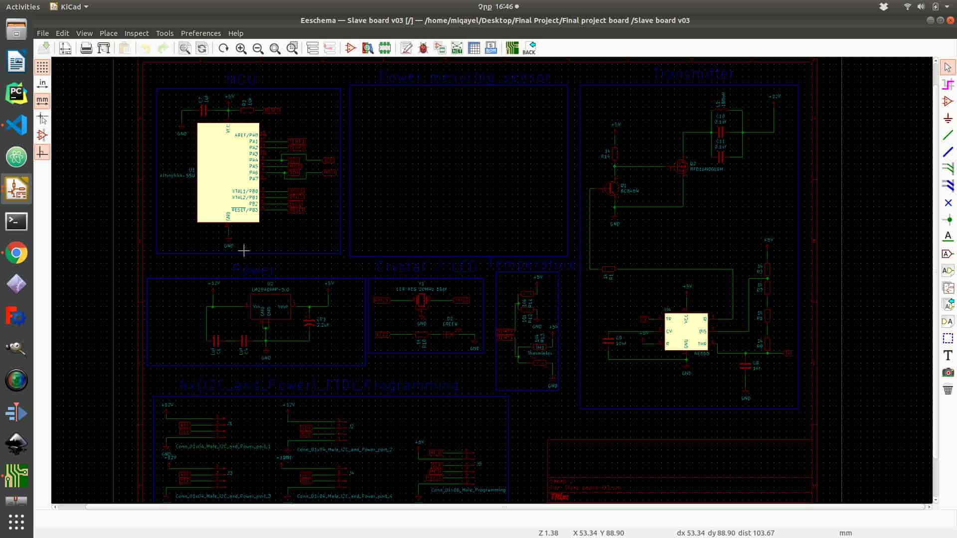
Schematics of slavea and master boards
For Schematics and layout design, I used KiCad PCB designing tool. I drow my schematics like block diagram, each block has its label, definitions, and function, and they are connected by “Place global label” function (you can find the icon on the right corner of the panel), it makes schematics more intuitive and understandable for investigation. It consists of 6 main blocks
Slave board
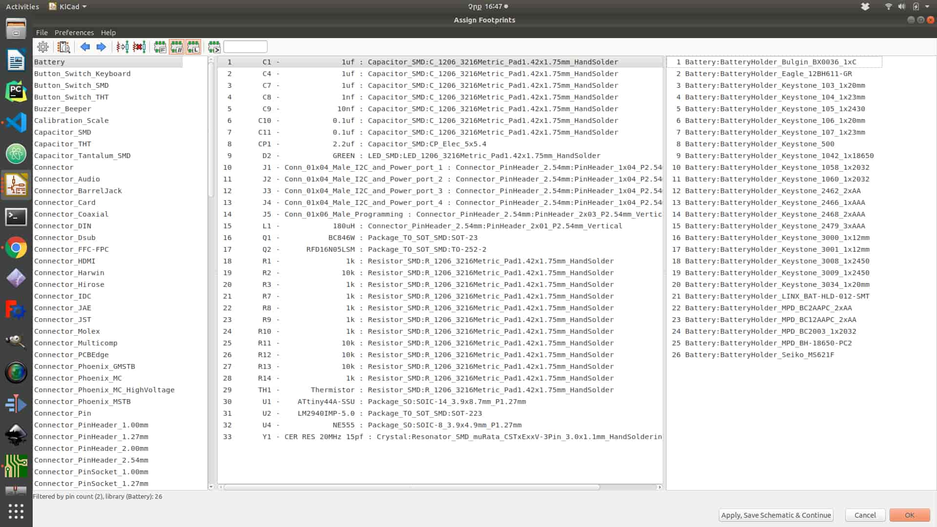
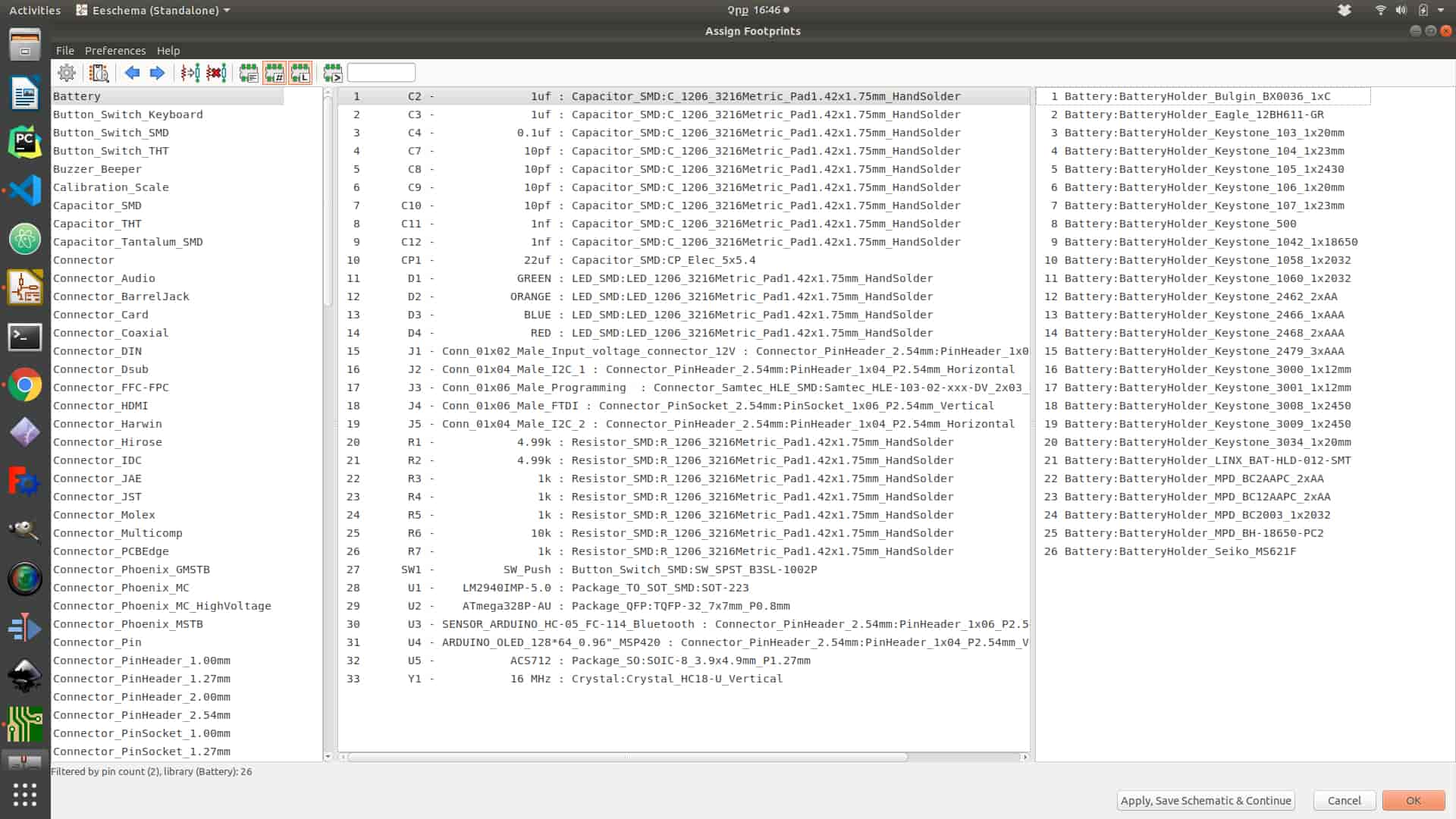
After checking all symbols, values, numbers, and connection between parts you can assign footprints for each part (choosing package) by going to “Tools > Assing Footprints”, after choosing a package for each component press “Apply, Save Schematics and Continue”.After click “Generate netlist” by clicking the icon on the top of the panel and finally you have done with schematics. You can go and start work on PCB layout if any problem appears you can go back to change and generate netlist again. If you what to know more how to draw schematics and reading datasheet go to week 7 “Electronics Design”.
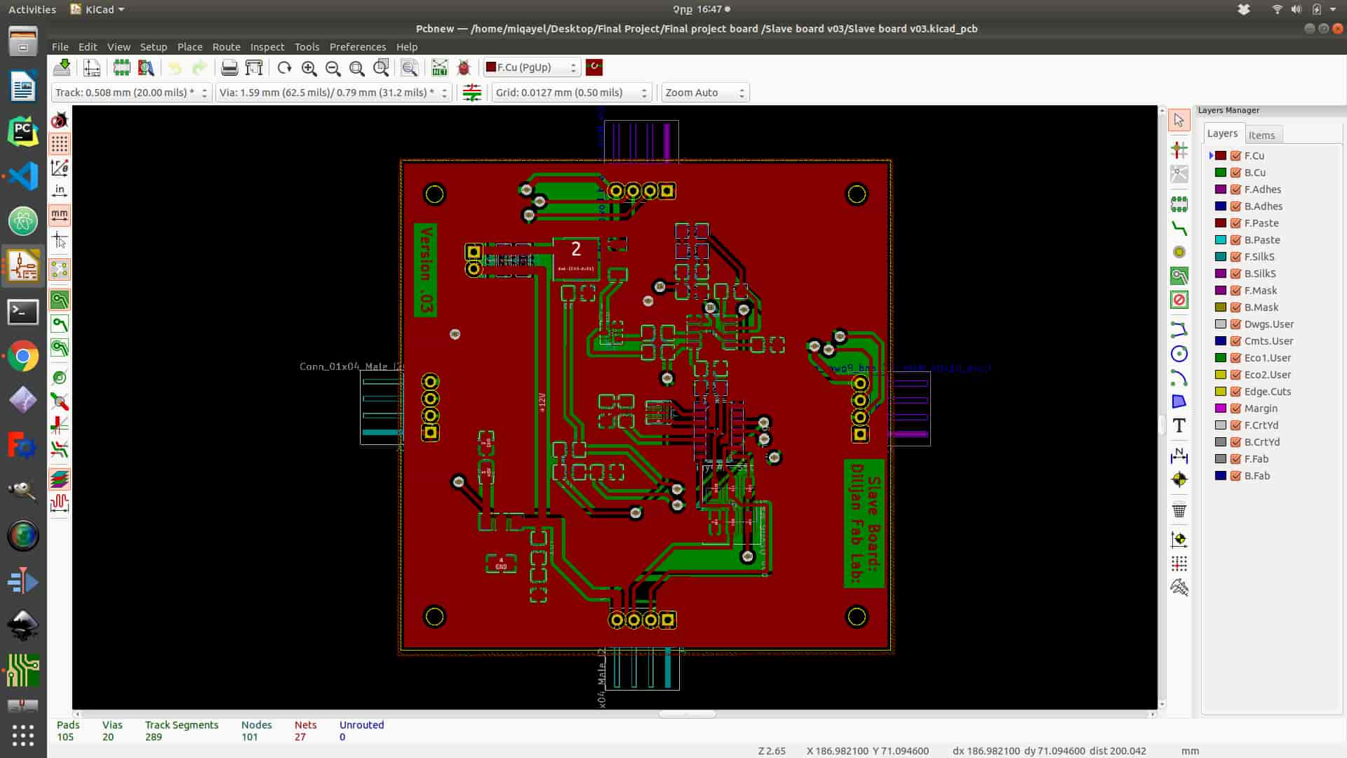
PCB layout design
To start layout design you need to click to “Run Pcbnew to layout printed circuit board” icon on the top of the panel. After the program opens the next step is to read netlist that you have generated in schematics program. To add all footprint for all components, you need to click “Read Netlist” icon on the top of the panel and click “Read Current Netlist”, and you will get all footprints. From this point, PCB layout design is started. First, you need to organize all the components optimally. In my case, I tried to use only one layer of the board but I have got a problem with the ground connection. I have solved it by connecting several jumpers in the process of soldering (It is not represented on layout design). After organizing all components (you can do it as blocks like in schematics) next step is connecting them together by choosing “Route tracks” function icon on the right side of the panel. Also, you need to set tracks thickness and Grid to avoid mistakes. In the process of milling your board, you can adjust grid on the upper side of the panel(I have chouse 10.00 mils (0.2540mm) it is not the same diameter as my tool (1/64 inch ) by it is ok ). After setting up the “Grid” next step is connecting components together. Couple advises for connecting
After connecting, the final step before exporting is to “Add Fill Zone ” by clicking the icon in the right corner of the panel and by choosing G(bkl), sketch outline and ground copper(at the same time it will do). And finally, you can export your board in .svg file format by going “File > Export > SVG…>(before clicking “Plot” .Print mode: choose Black and white, SVG Page size: Board area only, ) Plot ” it will save in the project folder.
G code
Before milling the board I need to generate g codes for traces, holes and cut out. I have generated all g code by using fab modules web version (for more information on how to use fab modules go to week 5 “Electronics production”). For milling the board I used “Roland SRM-20” milling machine, 1/64, 1/32 inch end mills.
For Information on how to solder the boards go to week 5 “Electronics Production”(the main difference is that I used 3 jumpers to connect all grounds area). Also, make sure that there is no short circuit on the board by using a multimeter.
At first I chose the program which can generate files for PCB milling . So I chose Fab modules which is perfect for exporting files for SRM-20 . Also there is desktop version which you can download on your computer but I used the web version which is very easy to use .
Import the image of your PCB In .png or another format .
Choose export format of the file . This is important because it must be readable for your machine . In my case I chose G-Code format which is working with different kinds of machines including SRM- 20 .There is also .rml file format which is exactly for SRM-20 and MDX-40 . But I used .nc or in another words G-code format in any case if your machine is different of mine .Choose 1/64 inch tool for traces .Adjust the parameters .In my case I haven't changed anything , I calculated it by default parameters . So after looking through parameters press calculate and wait . Press “Save” and save somewhere .Restart the page choose outline image and choose 1/32 inch tool for it (the file format is the same .nc ) . You can change the parameters , but I prefer to save it by default . And after saving the you got 2 files one for layout and one for cutout .
Board Milling
Clean up the area of machine , and board (make sure there is no oil on it).Make shure you got all tools
Stick Double-sided tape on the board tightly .Mount board inside the machine. mount board inside the machine .
Tight the tool in the spindle (By holding with the finger)
Before starting these steps you must read the manual .Open Vpanel for SRM-20 . Choose G54 in “Set Origin Point ” on the right side .Choose G54 in the left side .Go to Setup and choose “RML-1/NC Code ”. Choose the tool , at first 1/64 inches . (If you have not done it yet ).Tight the tool in the spindle.(If you have not done it yet ).Move the tool wherever you what to zero it .You can move it by using buttons in the middle +Y , -Y , +X , -X , +Z, -Z(be carefully with Z), you can adjust the speed of movement in “Cursor Step ” section . Press “X/Y” on the right side and click “Yes” , and press “Z” “Yes ” , it will change the origins by 0 .Make sure you have generated the files in Step 1 .Click “Cut” and press “Delete All”.Press add button and choose the g-code file . At first 1/64 inches file and press output .)Press “Red X ” , and the machine will start the milling proces .When it finish , press “View” button in the “Move” section .Change the tool to 1/32 inches . Zero the Z origin . Output the cut out file .And finaly will get the board .
Soldering
Clean up the space around .Make sure you have .
Make sure you have the electrical components . Remove unnecessary parts on the board with cutter . Clean up your PCB with water .Water the soldering iron sponge .Start Soldering
Solder by looking on schematics and layout .I added a jumper , after programming you can put it in one pin .
Programming
For programming my boards I have used Arduino IDE and Atmel Studio 7 invierment. I have uploaded all librarys form Arduino IDE and start programming on Atmel Studion 7 also I added Adafruit librarys for Oled display.
I2C communication code for Slave board
	/*I2C Slave Control
	Author: Miqayel Armayan
	*/

	 //libarary
	#include Wire.h>

	//Defines
	#define SLAVE_ADDR_1 1 //address: the 7-bit slave address (optional); if not specified, join the bus as a master.
	//First slave address is 1 , others 2,3 ...8.


	 //Variables Define


	 //--------------------------TH----------//
	int ThermistorPin = 0;//analog pin Termistor(ATtiny44a pin is other pin).
	int Vo;//integer to hold Termistor value
	float R1 = 10000;
	float logR2, R2, T;
	float c1 = 1.009249522e-03, c2 = 2.378405444e-04, c3 = 2.019202697e-07;
	//----------------------------------------------------------//


	void setup() {

	  Wire.begin(SLAVE_ADDR_1);                // join i2c bus with address #8
	  Wire.onRequest(requestEvent); // register event
	}

	void loop() {
	 delay(100);

	}


	// function that executes whenever data is requested by master
	// this function is registered as an event, see setup()
	void requestEvent() {
	Vo = analogRead(ThermistorPin);
	  R2 = R1 * (1023.0 / (float)Vo - 1.0);
	  logR2 = log(R2);
	  T = (1.0 / (c1 + c2*logR2 + c3*logR2*logR2*logR2));
	  Tc = T - 273.15;
	  Tf = (Tc * 9.0)/ 5.0 + 32.0;

	  Serial.print("Temperature: ");
	  Serial.print(Tf);
	  Serial.print(" F; ");
	  Serial.print(Tc);
	  Serial.println(" C");

	  delay(500);


	Wire.write(Tc); // respond with message of 6 bytes
	// as expected by master
	}
Oled display code for Master board
	/*I2C Master Control
	Author: Miqayel Armayan
	*/

	//libarary
	#include SPI.h>
	#include Wire.h>
	#include Adafruit_GFX.h>
	#include Adafruit_SSD1306.h>
	#include SoftwareSerial.h>

		   //Defines
		   #define SLAVE_ADDR_1 9//Slave address.
		   //oled defines
		   #define SCREEN_WIDTH 128 // OLED display width, in pixels
		   #define SCREEN_HEIGHT 32 // OLED display height, in pixels

		   // Declaration for an SSD1306 display connected to I2C (SDA, SCL pins)
		   #define OLED_RESET     4 // Reset pin # (or -1 if sharing Arduino reset pin)
		   Adafruit_SSD1306 display(SCREEN_WIDTH, SCREEN_HEIGHT, &Wire, OLED_RESET);

		   #define NUMFLAKES     10 // Number of snowflakes in the animation example

		   #define LOGO_HEIGHT   16
		   #define LOGO_WIDTH    16


			  #define Rx 0
			  #define Tx 1
			  #define LED_PIN 13
			  SoftwareSerial bluetoothSerial(Rx, Tx);


		   //Variables Define
		   int read_data;
		   int resistance;
			  int analogPin=1;//analog pin Power mesuring sensor


	void setup() {
		   //--------------------------Setup I2C data communication---------------//
	Wire.begin();        // join i2c bus (address optional for master)
	Serial.begin(9600);  // start serial for output
	//---------------------------------------------------------------------//


	//--------------------------Setup for OLED display----------//


	  // by default, we'll generate the high voltage from the 3.3v line internally! (neat!)
	  display.begin(SSD1306_SWITCHCAPVCC, 0x3C);  // initialize with the I2C addr 0x3C (for the 128x64)
	  // init done

	  // Show image buffer on the display hardware.
	  // Since the buffer is intialized with an Adafruit splashscreen
	  // internally, this will display the splashscreen.
	  display.display();
	  delay(2000);

	  // Clear the buffer.
	  display.clearDisplay();

	  display.setTextSize(1);
	  display.setTextColor(WHITE);
	  display.setCursor(0,0);

	  // draw a bitmap icon and 'animate' movement
	  //movingbitmap(logo16_glcd_bmp, LOGO16_GLCD_HEIGHT, LOGO16_GLCD_WIDTH);
	//----------------------------------------------------------//


	//--------------------------Setup for Bluetooth display----------//
	bluetoothSerial.begin(9600);
	pinMode(12,OUTPUT);
	//----------------------------------------------------------//
	}
	void loop() {
	for(int i=1;i<=8;i++){
	//--------------------------TH data----------//
	Wire.requestFrom(i, 6);    // request 6 bytes from slave device #1
	while (Wire.available()) { // slave may send less than requested
	char c = Wire.read(); // receive a byte as character
	Serial.print(c);         // print the character
	}
	//--------------------------HC-05----------//
	delay(500);
	Serial.print("Temperature: ");
	Serial.print(i);
	Serial.print(Tc);
	Serial.println(" C");


	//--------------------------OLED----------//
	val=map(analogRead(analogPin), 0, 1023, 255, 1);
	Serial.print("Power=");
	// Print incoming characters, if any, and keep track of the line and chars number
	if(val != -1){
	chars++;
	if(val == '\n' || chars == 21){
	lines++;
	chars = 0;
	}
	Serial.print(val);
	display.print(val);
	display.display();
	delay(10);
	Serial.println(" W");
	}
	}
	}