20. Project development
# 20. Project development
This is written in retrospect, but hopefully will capture the Final Project process that I went through.
Assessing Progress
My final project process began in earnest about two weeks prior to my presentation date. Up to this point, I had…
- A clear idea of the final project and the desired scope and form for the final device
- I had completed an initial concept design of the final project in Fusion 360…but understood that I needed to make significant modifications to deal with real world issues…including the physical and dimensional integration of components important to my final project (servos, neopixel strips, battery, etc.) and mechanical design for actuated parts.
- I had some work on electronics having made a Satshakit board (untested), accelerometer board (failed), RGB board (success) and light sensor board (success) in previous weeks…and have Eagle files for all of them.
- I had done very little to no programming work
Planning the Required Work
For me, ‘Supply Side Time Management’ (SSTM) requires a clear, holistic, well-organized understanding of all the tasks that must be done to achieve completion. Without this, SSTM is not possible and the completing the project in a short amount of time…would be futile. I began by listing absolutely everything that I could think of that needs to be done to complete the project…without worrying about organizing the list or generating duplicates. I made sure to do this on my PC and in my Git Repo…to allow for easy edits/organization later…and to ensure that I would have a back up of this important document. I used 2 software programs expensively in organizing the tasks…Freemind (a mindmapping program)
and Google Keep (a checklist program on my mobile phone and backed up in the Google Cloud…having a backup is critical!)
The list will not be complete or even sensible at the beginning, but I did this to get a reality check about the scope of the task ahead (it was pretty intimidating).
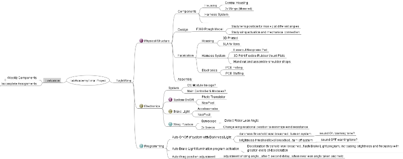
After running out of things to add to the list, I proceeded to organize it…quickly categorizing them into task groups: Device Design/Fabrication, Electronics Design/Fabrication, Programming, and Documentation. With this complete, I had a full and clear picture of what I would need to do…and I started my SSTM planning.
Rather than tackle each task group in order according to some prescribed time allotment, I chose to begin the first days of the 2 weeks touching every task…to refine my SSTM plan. I spent half a day on each task group, to better understanding of which group will require more…or less time than another. It became clear to me that Electronics and Programming are my weakness…and would require more time allotment than Device Design and Documentation.
Triage
The task plan completed, it became clear that I would have to reduce the scope of my final project to finish on time. Reluctantly, I cut out functionality from my final device to arrive at the simplest acceptable minimum scope for my project:
- Utilize only the Light Sensor (Phototransistor) as my Input Device
- Simply have the input device trigger an automatic ON state of 2 output devices…Neopixels and servos
The essence of my project…is to improve the visibility of motorcyclists when they ride at night. My solution to this problem is to increase the motorcyclist’s visibility by increasing rearward facing illumination from the rider…a bright light that would supplement the rear light array of the motorcycle…a wearable device that would make a motorcyclist easier to see from a distance. My triaged ‘miminum functionality’ still meets these objectives.
In the early days of the 2 week work week, I admittedly held hope that I would be able to add other functionality to my device…but after all, even this ‘minimum functionality’ version of my device was nearly impossible for me to complete on time.
Completing the Tasks
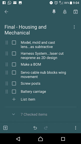
Device Design/Fabrication
In the end, I began by working on Device Design. The final device shape and dimensions would be critical in the size and locations of the electronics that it will contain. With an understanding of what electronics I would need however (from my list of tasks), I knew to make space provisions for those eventual components in the device design as well. In Fusion360, I modeled up every component that the device will have to contain in real dimensions and simultaneously worked on the final “shell” form for the device itself. With a reasonable shape to contain everything generally achieved and mechanical components drafted…I 3D printed the first prototype of the final project (using PLA) via F360 generated STL files and gcode generated by Prusa Slicer for my Prusa MK3 i3 3D printer…and moved on to Electronic Design/Fabrication.
Electronics Design/Fabrication
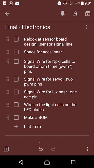
Understanding that it is not enough for me to simply replicate the Satshakit…but knowing that I do not have the knowledge or skill to design a Microcontroller Unit (MCU) from scratch…I chose to modify the Satshakit design to more specifically suit my project. With the base schematic and board design in Eagle previously drawn up, I added…
- 6-pin ISP programming header (which proved indispensible!!!)
- 3-pin connector for my Light Sensor (located separtely from the MCU)
- 7-pin I2C connector for future functionality additions
In addition to the MCU, Electronics Design/Fabrication for my final project also required…
- A Power Junction Board…to be connected with and receive power from a rechargeable battery pack…into which the MCU, 2x Servos, 3x Neopixel light cells will all plug
- A remote sensor board…the light sensor needs visibility to the sky and the future accelerometer needs to be positioned on the top of the device.
Eagle schematic and board routing work is procedural for me at this point…but my minimal understanding of electronics meant that I was uncertain if additions I was making in the design of my boards were correct. Routing for the extra pins on the MCU board could not successfully be done on top of the board (I would eventually have to correct for missed connections…ground lines and reset lines…by soldering on wires) and some connections were completed under the board by soldering the base of the pins together. For the Power Junction Board…I replicated the power signal smoothing circuitry from the Satshakit board. For the Sensor board, I replicated the circuitry of Neil’s light sensor board. Without knowing enough about electronics, my strategy was to ‘hack in’ electronics features that I know works from boards designed by experts. With Eagle design work completed, I milled the PCBs and stuffed them with components…again, this has thankfully become comfortable and procedural for me at this point in the FabAcademy course. With the first stage of Electronics Design/Fabrication completed, I proceeded to programming to activate the boards.
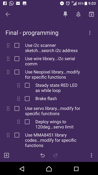
Programming
And here I meet my Nemesis…Programming. While I have programmed before (Basic and Pascal) and understood the basic structure of programs, I am unfamiliar with the syntax of modern computer languages. Throughout this course, I have tried to study programming when I can…especially C (particularly Elliot William’s book “AVR Programming”), which Neil recommends as an efficient program for microcontrollers. Unfortunately, I was never able to put the required time into this study to give me adequate proficiency. For my final project, I decided to do my programming work in the Arduino environment.
Before getting to functional programming for my device, I needed to make certain that the MCU board I made is functional…can be utilized as an Arduino clone. Using an Arduino Uno as a programmer and utilizing the ISP pins I added (and self-made ISP connector!), I uploaded the Arduino bootloader on my MCU.
The procedure as follows:
- Connect the Arduino Uno to the PC via a USB cable
- Upload the ‘ArduinoISP’ sketch (number 11 in the Arduino IDE’s Example sketch list) onto the Uno…turning it into a ISP programmer
- Connect my MCU board to the Uno using an ISP cable…important!!! A 10uF(?) Capacitor must be inserted into the Uno, bridging the GND and Reset pins…to make ISP programming possible
- In Arduino IDE’s ‘Tools’ menu choose ‘Arduino Genuino/Uno’ as the ‘Board’, ‘Arduino as ISP’ as the ‘Programmer’ (be careful here…there are other similar option ‘ArduinoISP’ and ‘ArduinoISP.org’ which are not correct choices) then select ‘Burn Bootloader’ (at the bottom)…this essentially turns the MCU board into an that the ISP connection is incorrect. Check that MOSI, MISO, SCK, RESET, VCC and GND pins are correctly connected. (In my case, I discovered that neither my Reset nor GND pins were corrected connected in my board design…requiring a fix by soldering bridging wire).
- With the ‘Bootloader’ uploaded to the MCU, any Arduino sketch can be uploaded to the MCU. Open the sketch you want to upload to the MCU…then in the ‘Sketch’ menu, choose ‘Upload Using Programmer’ or use the key combo Ctrl+Shift+U to upload the sketch to the MCU (the right arrow button typically used to upload sketches will NOT work).
- Unplug the USB cable from the PC, the ISP cables between the Arduino and MCU…and now the MCU can be used to drive Input/Output devices using Arduino sketches
Similar to my approach on electronics, because of my shortage of applicable knowledge, I chose to utilize example and other sketches made by professionals and is known to function as the basis of my final program. I chose to approach programming methodically my completing small task, specifically…
- Test MCU communication with the Light sensor…see if the program can see serial data output from the Sensor
- Test MCU communication with servos…see if the program can make servos move to specific rotational positions
- Test MCU communication with neopixels…see if the program can turn ON and Off the neopixels and change colors in the way I hoped
- Test Light sensor activation of servos…see if setting a specific light sensor level can move the servo spindle to a specific rotational position
- Test Light sensor activation of neopixels…see if setting a specific light sensor level can move trigger the running of a specific, dynamic neopixel illumination program
- …then lastly, combine the last two tests into a single program…where a specific light reading from the Light Sensor would trigger the neopixel to turn ON and the servo to move its spindles to a specific rotational position
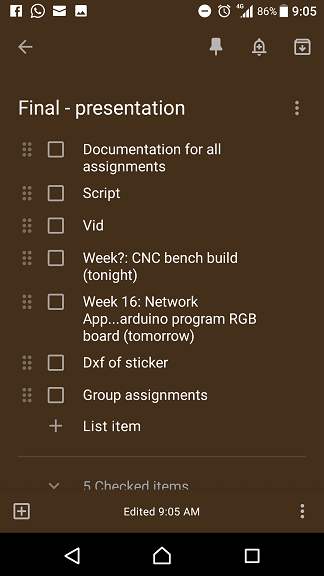
Documentation
As often suggested by Neil, I documented as I went…and went so far as adding extra webpages to my FabAcademy site to record my thoughts and learnings for the task categories I defined (Device Design, Electronics, Programming). I am not certain I will keep these pages around in the end…but it was good for me to NOT have it all on one page and have it get unweildingly large…and a source of added anxiety for me (having to scroll through everything to get to something I need to find). I also created a number of folders in my repo to contain images, Fusion files, Eagle files, Arduino files, etc....specific to the final project.
I also did as Neil suggested and immediately uploaded a draft slide and video to test the procedure required for the final versions of both. This ‘touching’ of the final presentation procedure proved to reduce the anxiety of uploading final versions on the final day significantly
In addition to keeping up digital documentation, I also kept a single notebook to jot down any random notes as they occur to me…making sure to date the pages and keep the writing and diagrams as legible as possible. It is important that it is a single notebook…rather than many scraps of paper or several notebooks…because it helps to keep things a little more organized and reduces the extra stress that would come with trying to remember which piece of paper or which notebook some thought was recorded into. This notebook proved indispensable for me as a workbench companion…to make instant notes that can be recalled a few minutes or a few days later…and can be very useful in a more refined digital documentation later. The danger here…this notebook must be protected…as lost or damage would be devastating to moral and a big setback to the rushed final push process.
Learning Outcome
Even with the best planning I could come up with and allowing as much time to the tasks as I could (while balancing other aspects of my life), I could barely get my final project to at 95% completion state. Here is a list of some of the things that didn’t go to plan and things I learned…
- Starting the work period by ‘touching’ every aspect of the major work task categories was a GREAT idea…as it gave me a very realistic expectation of the work that will be required. The reality is often very different from my theoretical planning.
- Remain disciplined about time management. When you have run out of time on one task and are scheduled to do the next…stop what you are doing and move on. For me, this went against my instincts to finish what I started or get things perfect…but it was my resistance to keep on schedule that caused me to come close to not finishing my project at all.
- Work carefully, methodically and neatly…but DON’T try to make everything perfect from the beginning. This wastes valuable time needed by other tasks…and more often than no, the same task will need to be redone because of redesign or other issues revealed by other tasks.
- Seek perfection in the final stages…as much as time allows.
- 3D printing prototypes is a great idea, as it reveals in physical form what might not be so obvious in a virtual 3D model…but reprints takes time…and time planning to make good use of printing time needs to be done (do electronics or programming or documentation work instead)
- The speed of 3D printing can be dramatically increased by making adjustments to the printing parameters…specifically the print layer height (0.3mm), the amount of infill (10%) and avoiding supports where possible. These ‘draft’ quality settings on the prusa printer generates still strong and usable prototype components in a much reduced amount of print time. Also, on the Prusa, the print speed can also be adjusted ‘on-the-fly’. I learned to leave the speed at standard 100% for the first 5% of the print…to ensure a stable base. Then, depending on the complexity of what is being printed (straight vertical is simple) I will increase the speed up to as much as 300%. Simultaneous to the higher speed, I will increase the nozzle and bed temperature a bit. The result is a less than clean surface finish…but good enough for prototype form.
- For electronics schematics, spend the time to give names to the pins that will have meaning to you. For example, I added ‘PWM’ to certain pin names knowing that the servos will need those pins and doing so will make identification of those pins on the board image easier to find.
- For electronics trace routing…split the work into two main work…power and data. I learned that with power, all devices connected must share a common GND line and both VCC and GND traces should be made a wide as allowable…to decrease resistance. Type ‘Show’ and follow with ‘GND’ or ‘RESET’ to highlight those items in Eagle board design. Data traces should be kept as thin as reasonable, to avoid signal noise issues.
- The most difficult as aspect of electronics work for me…was the difficulty of wiring making and physical routing management within a mechanical device. Many times, the wires and connectors were poorly made (my lack of skill) or were too short (I didn’t consider how they would respond to movement of actuated parts…or even the need for some leeway when I need to make connections). The location and positions of connectors also needed more thought than I gave it. Poorly located connections caused difficulties in plugging power or signal lines in.
- Soldered connections are VERY fragile. How a pin is soldered onto the board and how often it would come under stress from connections made and unmade should be carefully considered. Broken solder joints will result in hard to discover device non-function issues.