11. Input devices
The topic of this week is “input devices”. This week and next week topics (Output Devices) are very important for my final project. The class video is here.
Assignments
- individual assignment:
- measure something: add a sensor to a microcontroller board that you have designed and read it
- group assignment:
- probe an input device’s analog levels and digital signals
In the group assignment, we tested the analog levels and digital signals of sensors with using lab’s oscilloscope. Pleae also see our week 11 group assignment page.
I am get used to make some sensor devices with Arduino. Therefore, I tried to make the board which have two different sensors and write the program to read valuse of both two sensors (A/D converting in two different pins at the same time).
1st Challenge: Light and Accelemetor Sensor
I choose the following sensors to add on my original board.
- Light: PT15-21C/TR8 (Phototransistor)
- Accerometer sensors: ADXL343BCCZ
Datasheet of ATTiny44.
I used ATTiny44 in this board. The datasheet is helpful to check out pin configurations, which pins I can use for A/D convertion.
The following figure show the pin configuration of ATTiny 44.
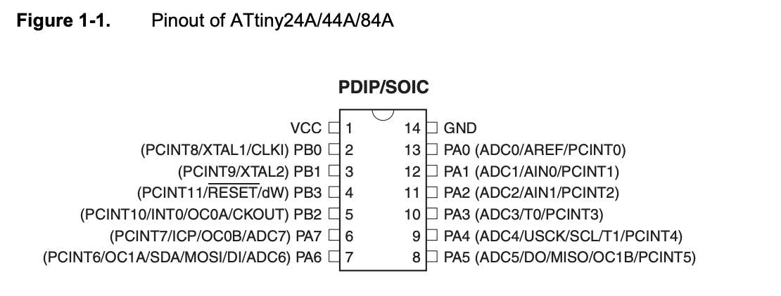
ATTiny 44 have seven pin configuration of ADC (PA0~PA7). Therefore, I could connect those pins to ADC out of each sensors.
As learned from week 9 (Embedded Programming), the direction of those pins should be configurated as “input” to read analog values from sensors. For example, if I want to read the value of the sensor that is connecte to PA7, it should be configured as follow.
in C language:
DDRA = (1<<PA7)
Designing PCB on EAGLE
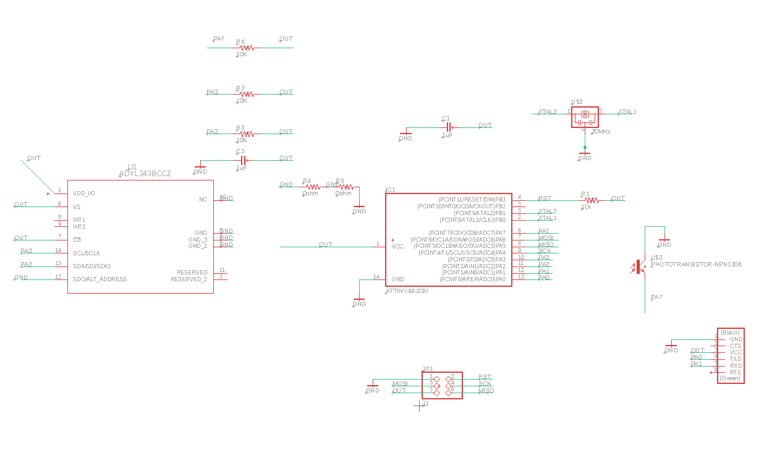
First, designing PCB on Autodesk EAGLE. I will use the following parts.
- attiny44
- Phototransistor
- ADXL343BCCZ-ND
- Footprint for EAGLE could be downloaded from here
- 10K ohm register x 4
- 0ohm register x 2
- 1uF Capacitor x 2
- 20MHz Resonator x 2
- 2x3 Jumper Printed
- 6 pin FTDI Header
The schema is here:
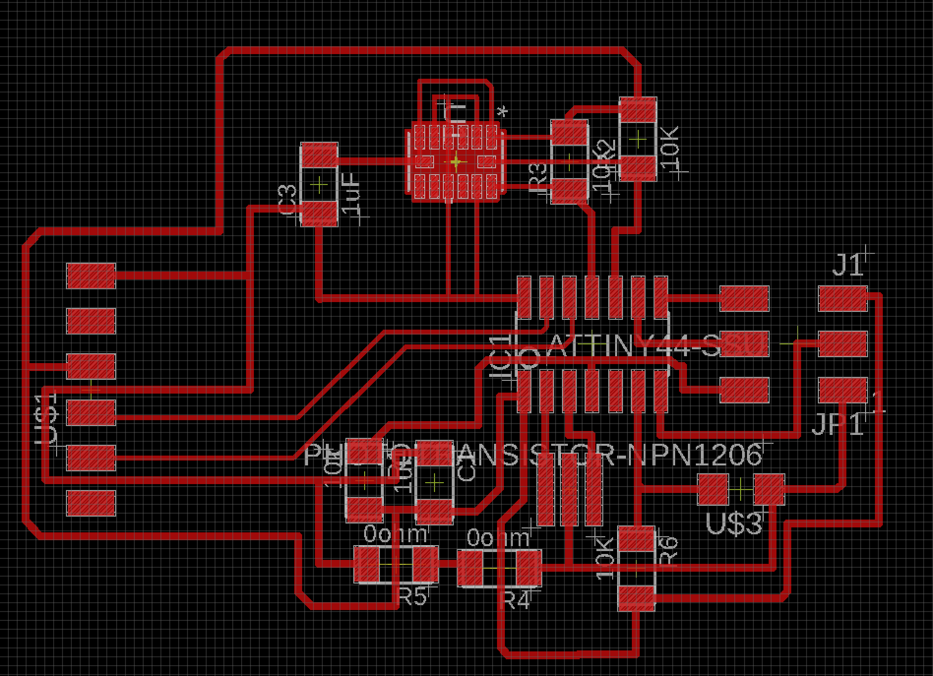
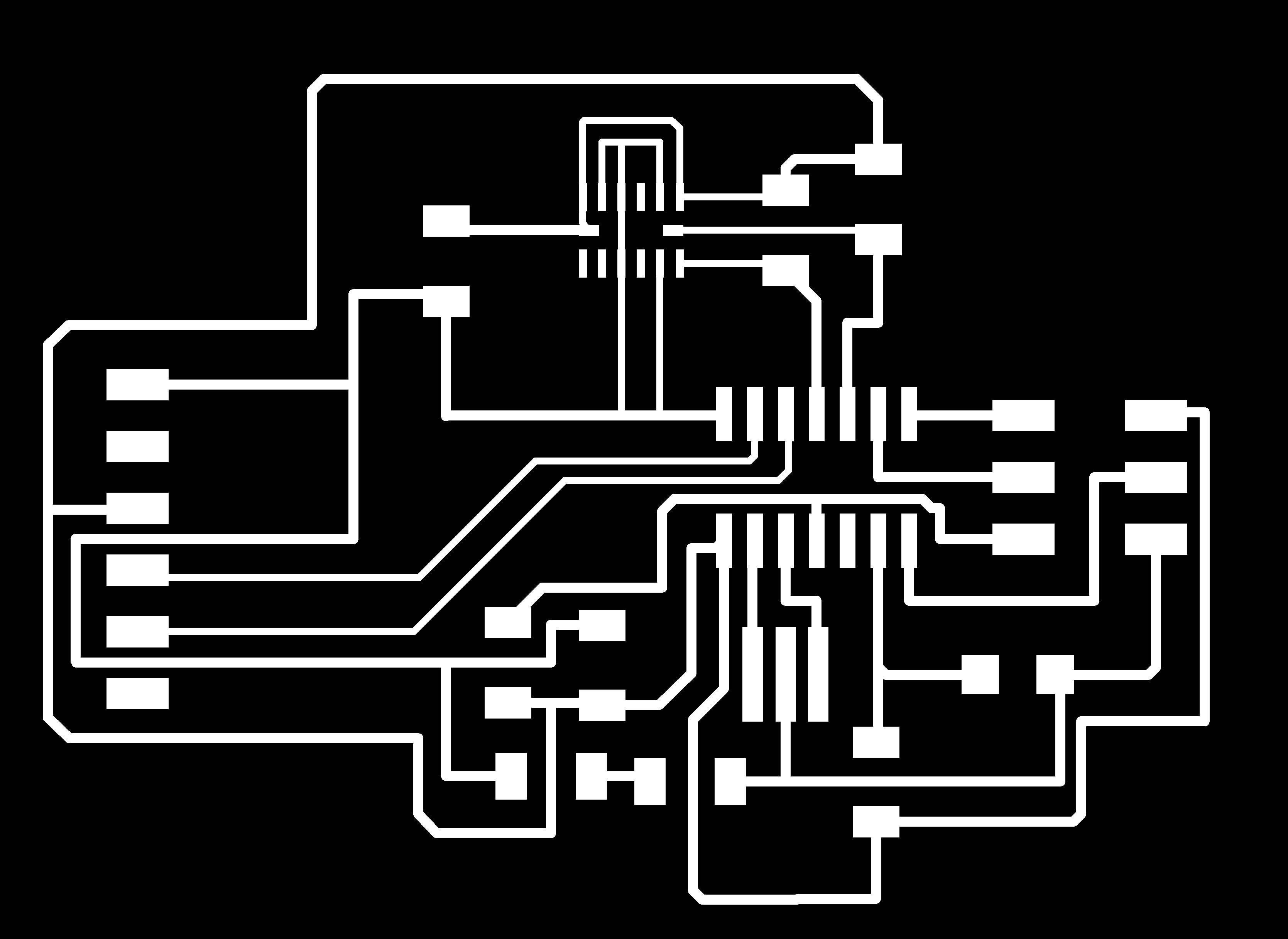
The board design is here:
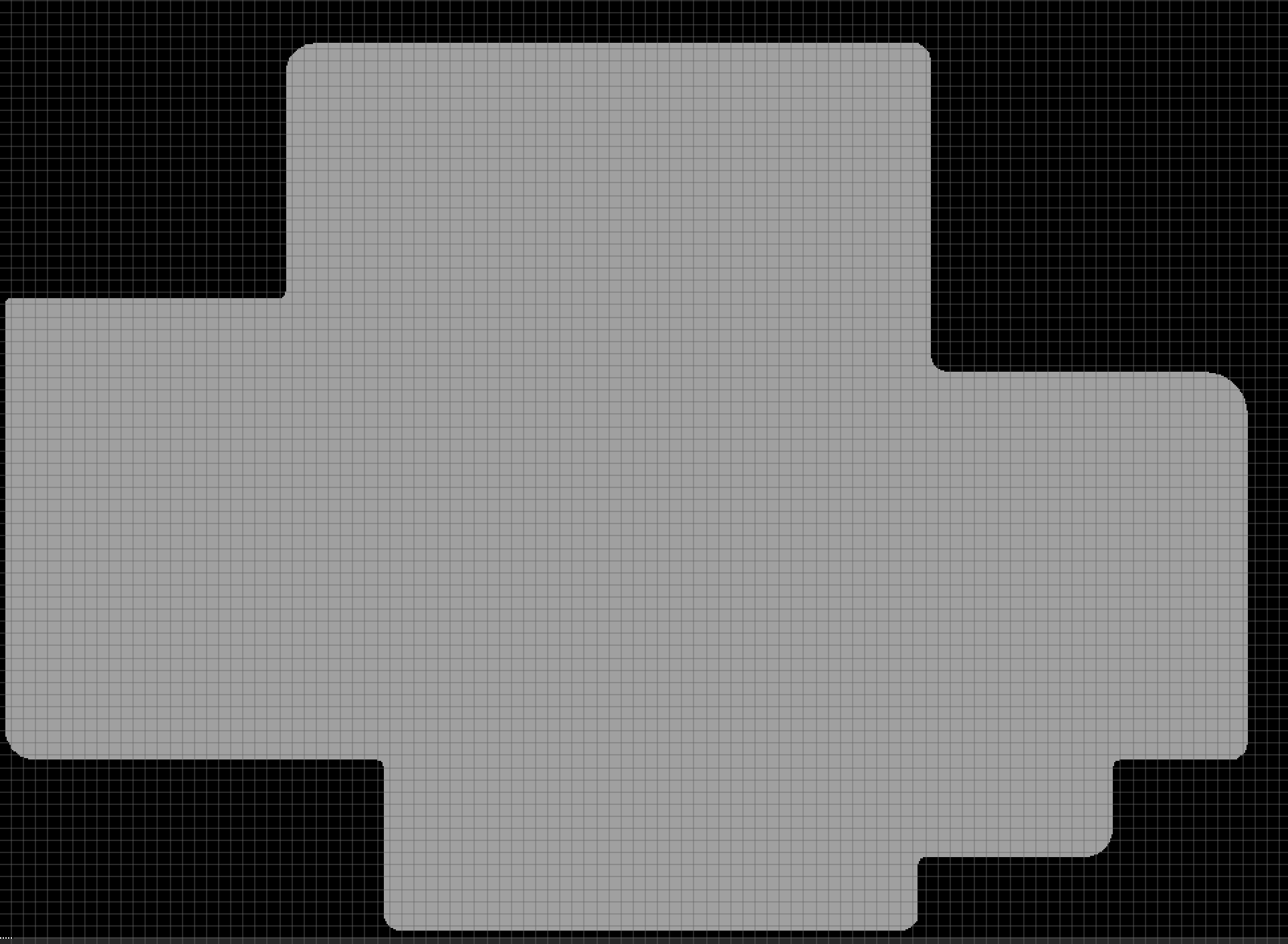
And, I will also design the outward form.
Export to PNG files.

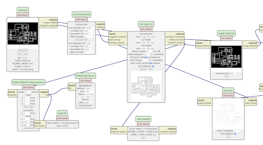
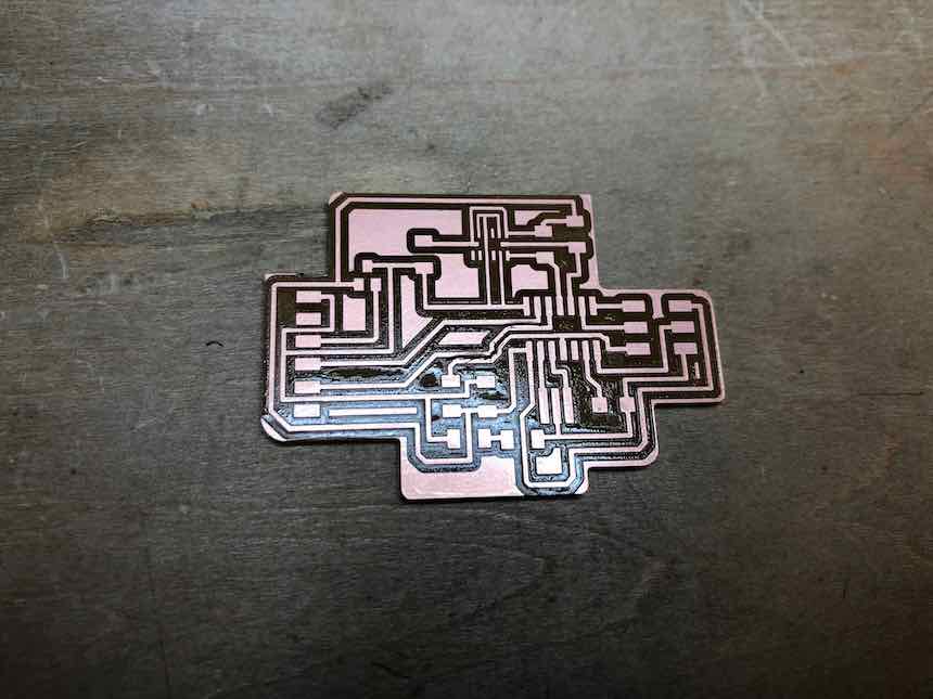
Then, import to the mods and make CAM file for milling by Roland SRM-20.
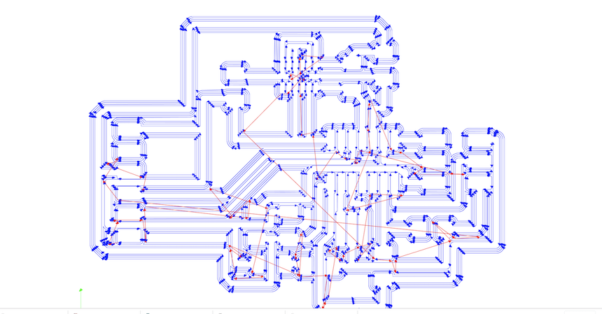
Before going to milling, I checked whether the patterns could be cut correctly.
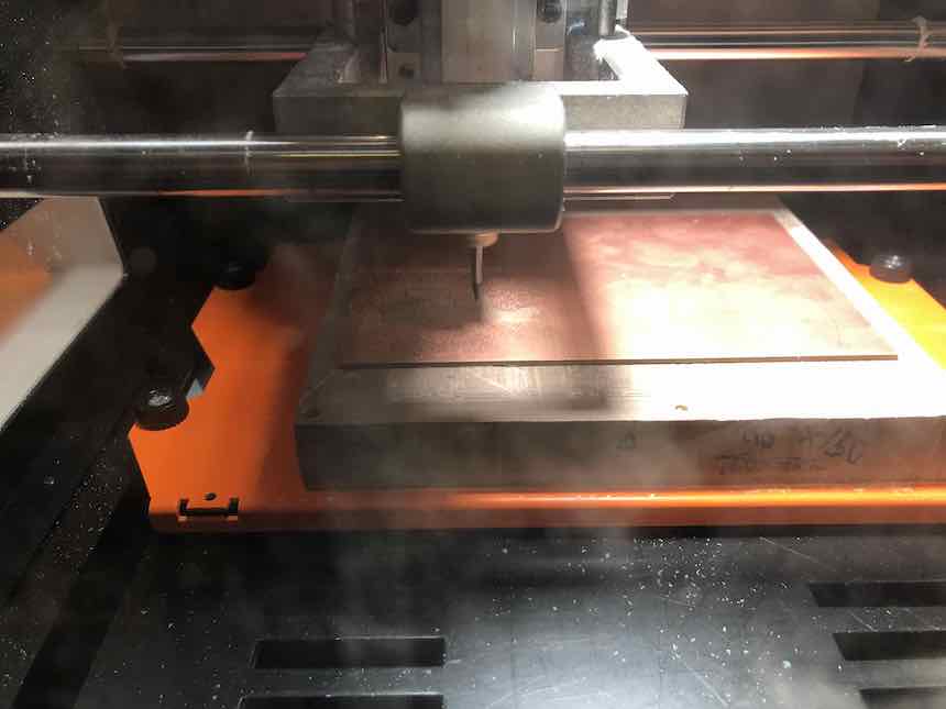
OK, it’s time to move for milling.
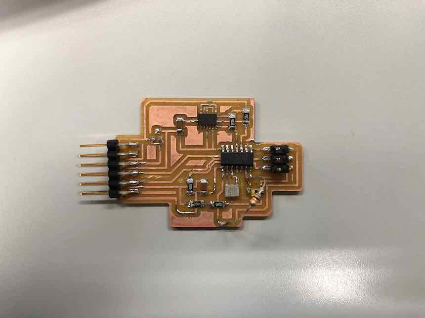
Then, it’s completed to make a board. And, I will soldering components.
Soldering is completed.
Programming
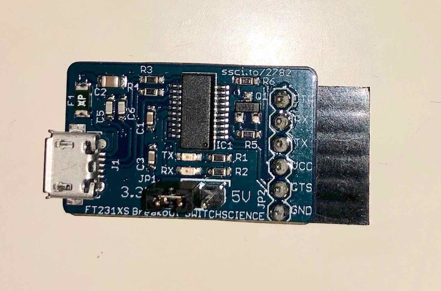
I will use this FTDI connector. It could switch the supply voltage in 3.3V and 5V. I set 3.3V to connect my board and my PC.
I wrote the following code in Arduino to check whether the phototransistor works or not.
#include <SoftwareSerial.h>

SoftwareSerial ss(0,1);
const int LIGHT_PIN = 7;

void setup() {
  // put your setup code here, to run once:
  ss.begin(9600);
  pinMode(LIGHT_PIN,INPUT);
  //analogReference();

   //
   // set clock divider to /1
   //
   CLKPR = (1 << CLKPCE);
   CLKPR = (0 << CLKPS3) | (0 << CLKPS2) | (0 << CLKPS1) | (0 << CLKPS0);

   ADCSRA = (1<<ADEN)
    | (1 << ADPS2) | ( 1 << ADPS1) | (1 << ADPS0);

   //TCCR0B |= (1<<CS01);

}

void loop() {
  // put your main code here, to run repeatedly:

  int val = analogRead(LIGHT_PIN);
  ss.println(val);

  delay(100);
}
The result, I checked with Serial monitor.
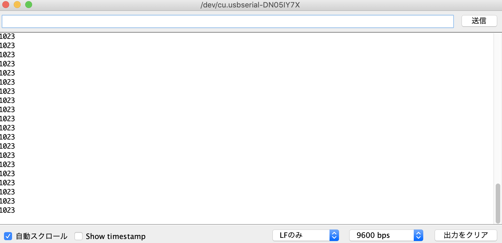
But the value of the light sensor always shows 1023....
According to the instructors, the problems of this board are…
- 3.3V regulation. 3.3v regulator should be connected only to accelemetor, and it is better to let microcontrollor work in 5.0v. However, my circuit designed whole in 3.3v.
- I choosed different type of photo-transistor (light sensor), that could buy in local shop in Japan (not digikey). Therefore, the value of pull-up register would be different, and I should ckeck the datasheet for choosing appropriate value of register.
- Accelometer has SCL/SDA pins and those require I2C communications to read the values of sensor. I misconfigured to assigned the pins of the accelometer (those should be connected to SDA to PA7, and SCL to PA4).
2nd Challenge: Light and Hall Effect
I couldn’t fix the problems of the accelemeter and lignt sensor board described above. Moreover, accelemetor chip (ADXL343) is quite difficult to soldering. Therefore, I changed to make different board that is added light and different sensor.
I choose hall effect sensor (620-1403-ND).
Datasheet of ATTiny45
This 2nd challenge, I decided to follow to class sample boards. Therefore, I used ATTiny45. ATtiny45 is almostly the same with ATTiny44, however the number of pins in ATTiny45 are fewer than those of ATTiny44.
As same with ATTiny44, I checked the datasheet of ATTiny45 to find out which pins are assigned as A/D converters.
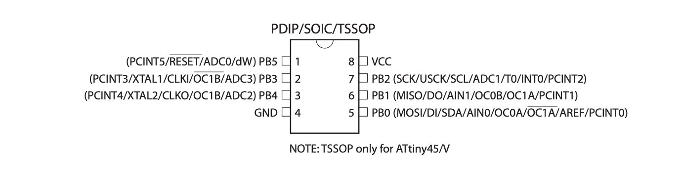
According to the pin configuration of ATTiny45, PB2, PB3 and PB4 are assigned as ADC. Therefore, I could connect those pins to the sensors.
Circuit Design.
In the 2nd challenge, I am combined the following two sample board (board for hall effect and the board for photo-transistor) provided in the class.
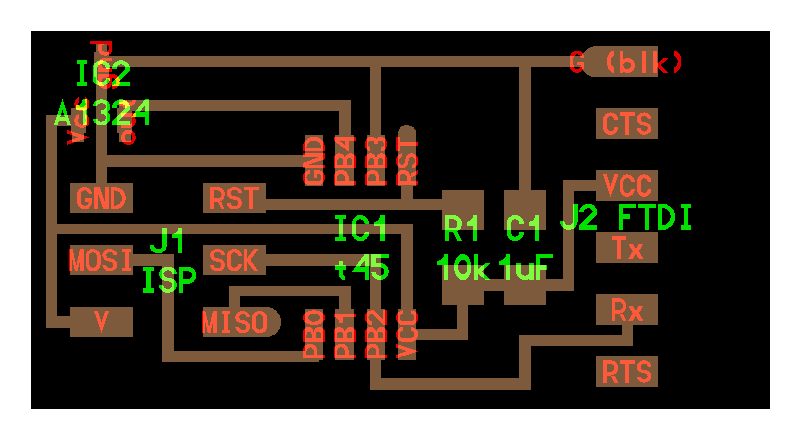
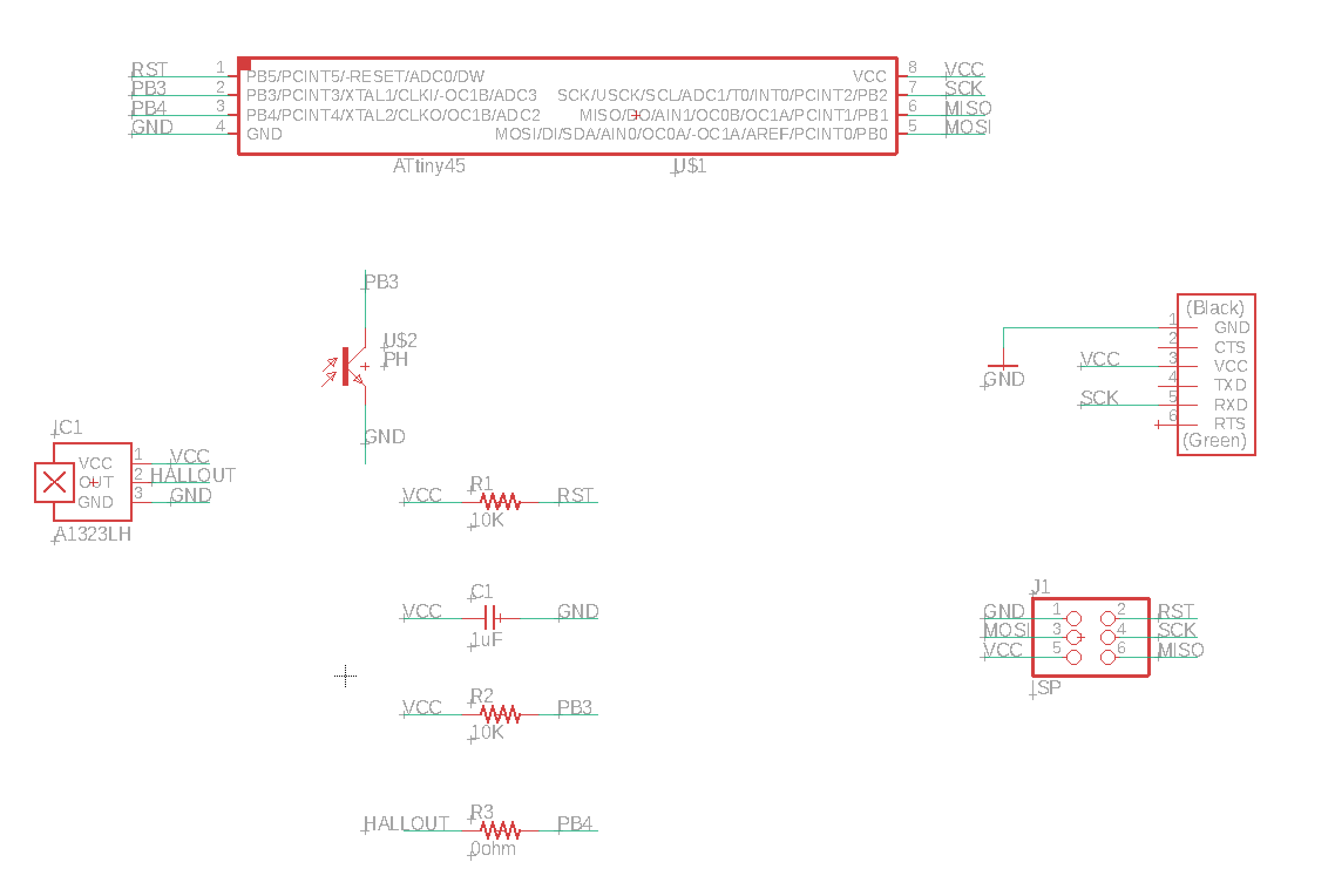
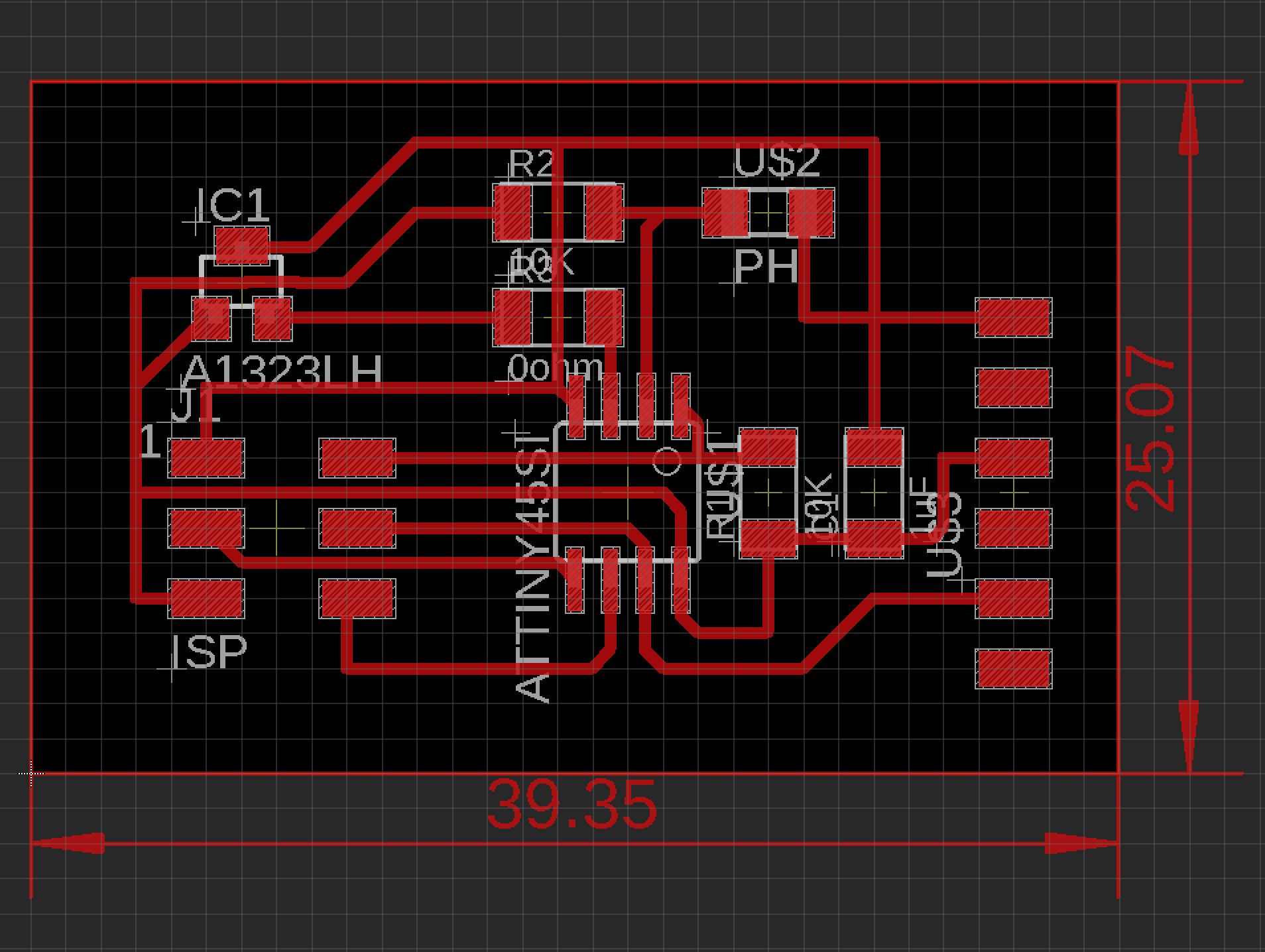
In these sample boards, PB4 in ATTiny45 is connected to Hall Effect and PB3 is connected to photo-transistor. Here is the shecma of the 2nd board by Eagle.
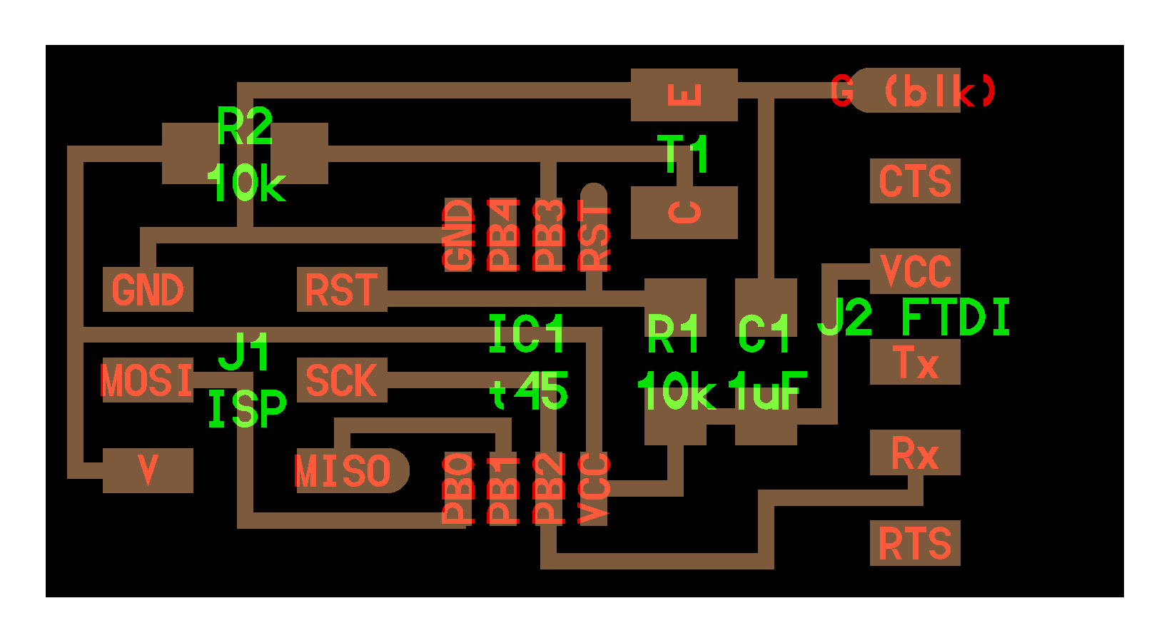
And, here is the design pattern of the board.
Before moving the milling section, I checked whether my board works well or not with using Breadboard. And, I confirmed the sensor workd well.
Milling and Soldering
After checking in breadboard, and also checking ERC/DRC, I exported the design of the board to PNG.
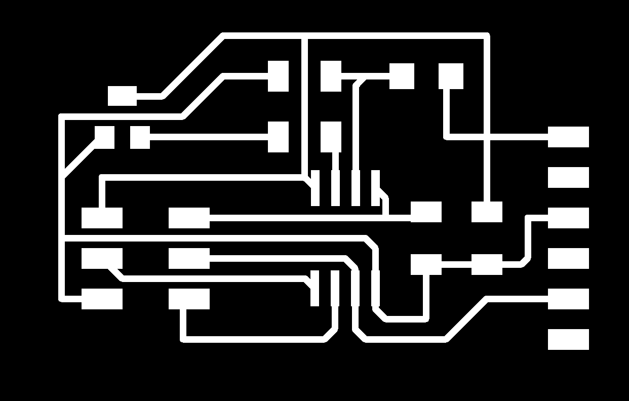

Then, making CAM file of the circuit in mods.
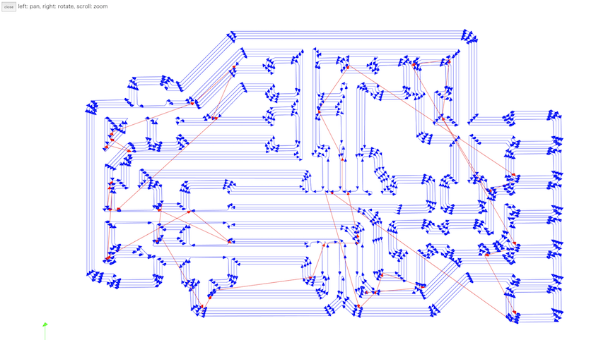
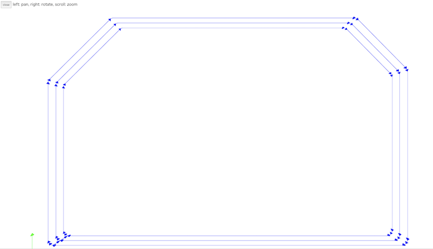
Here is the view of the path for milling by Roland SRM-20. From the experience of week 7 (Electronics Design) assignment, I checked the path carefully before moving to milling part. That looks fine (no pathes that are not overlapped.)
Also, making CAM file of the outline of the board.
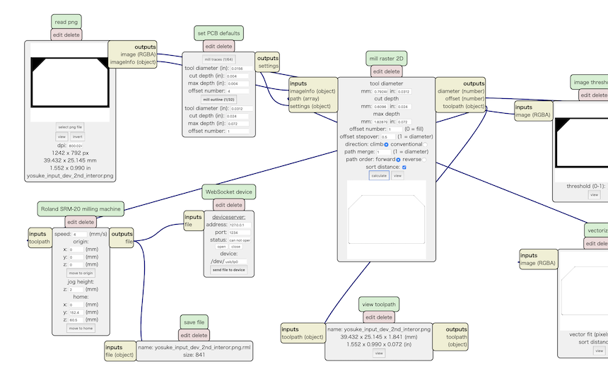
And, it’s also corretctly made the path for milling.
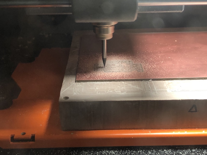
Then, milling PCB.
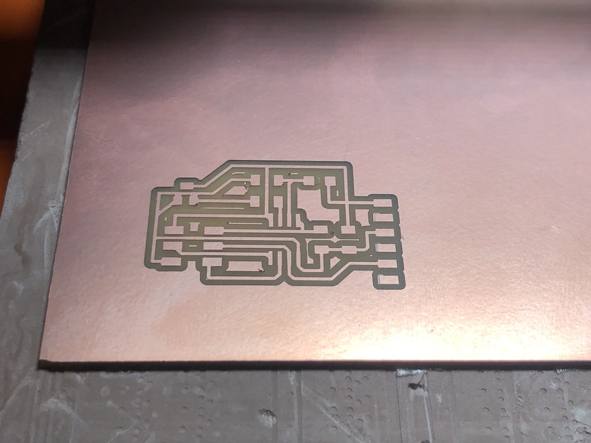
After milling the board, I solidered each parts.

In this board, thise parts are required.
- ATTiny45 Microcontroller x 1
- 10k register x 2
- 0ohm register x 1 (for jumper)
- 1uF Capacitor x 1
- Hall Effect Sensor x 1
- Photo transistor x 1
- 2 x 3 pin for ISP connection
- 1 x 6 pin for FTDI connection
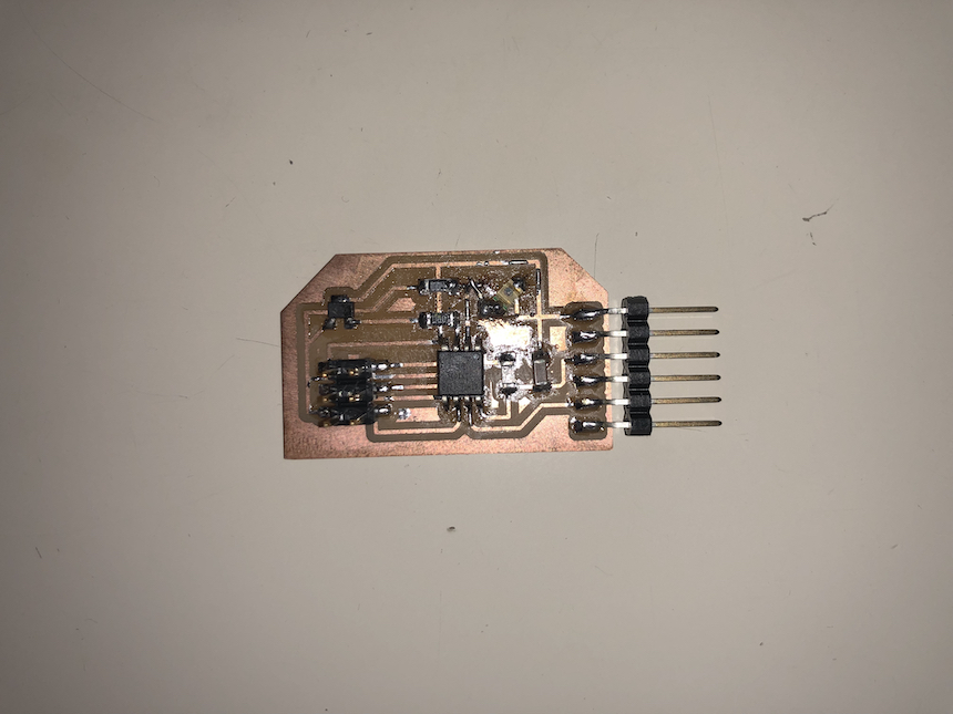
I took some mistake when soldering photo transistor again and again, so the copper circuit around phototransistor was broken. Then, I made a bypath near the photo transistor and solderied it.
Programming
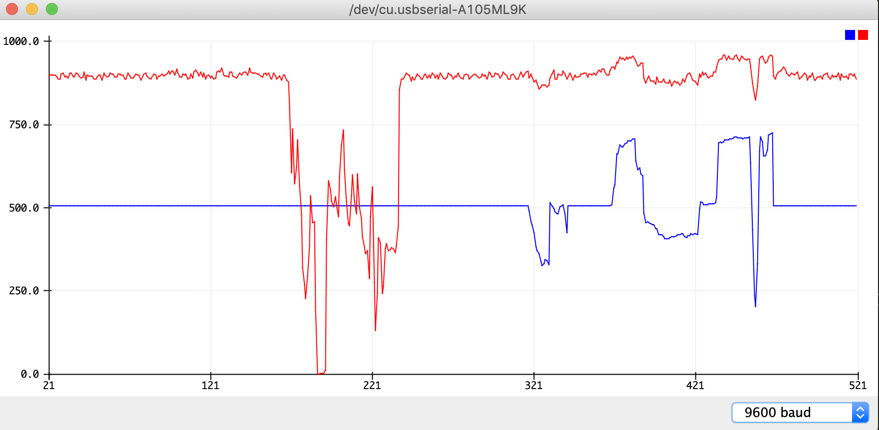
It is required to show values of both hall effect and light at the same time. However, it is very easy to write such a program in Arduino. If we want to get the value of A/D converted data, we just define the pin number which is connected to the sensor, then write:
int val = analogRead(A3);
I just simply wrote the following program:
#include <SoftwareSerial.h>

const int lpin = A3;
const int magpin = A2;

SoftwareSerial ss(1,2);

void setup() {
  // put your setup code here, to run once:
  ss.begin(9600);


}

void loop() {
  // put your main code here, to run repeatedly:

  int val = analogRead(lpin);
  int val2 = analogRead(magpin);

  ss.print(val2);
  ss.print(',');
  ss.print(val);
  ss.print('\n');
  delay(500);

}
Then, uploaded the sketch to the board, and opened the “serial plotter”, that show values of analogReaded data on the line chart. That works well.
Week 11 files
1st trial.
- Electronics Design
- Program
2nd trial.