Assignment
GROUP ASSIGNMENT:
compare the performance and development workflows
for other architectures
INDIVIDUAL ASSIGNMENT:
read a microcontroller data sheet
program your board to do something,
with as many different programming languages
and programming environments as possible
What I did
- Learned basics of embeded programing
- Started using arduino
- Learned to add custom libraries to arduino
- learned to program IC using arduino
INTRODUCTION
This week we have to program Hello-echo board that we designed in Electronics production week. I have very basic knowledge in programming. I have to learn from the basics. This week I will learn to program echo board using Arduino, C and assembly language.
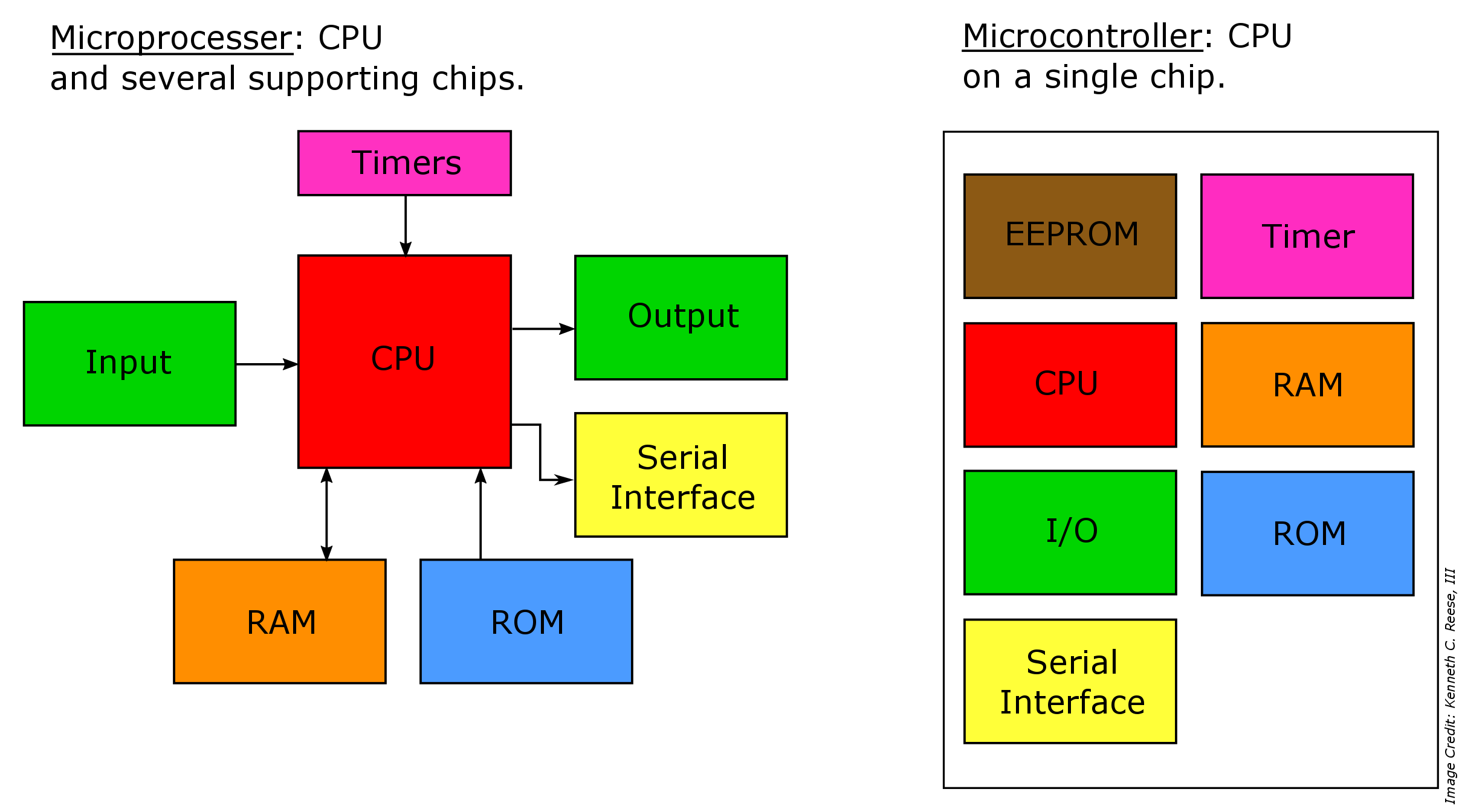
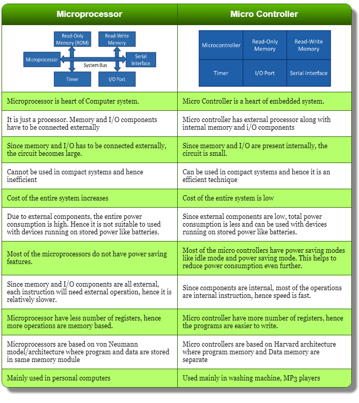
Microcontollers VS Microprocessors
 source
Microcontrollers (MCUs) tend to be less expensive than, simpler to set-up, and simpler to operate than microprocessors (MPUs).
An MCU can be viewed as a single-chip computer, whereas an MPU has surrounding chips that support various functions like memory,
interfaces, and I/O. The MCU vs. MPU question may seem simple, but there are some prominent differences.
 source
ARCHITECTURES
- Harvard architecture
- Von Neumann architecture
- CISC
- RISC
- PIC
- AVR
- SRAM
- Flash memory
- Registers
The Harvard architecture is a computer architecture with physically separate storage and signal pathways for instructions and data, so it can simultaneously use both busses.
The design of a von Neumann architecture machine is simpler than that of a Harvard architecture machine, which is also a stored-program system but has one dedicated set of address and data buses for reading data from and writing data to memory, and another set of address and data buses for instruction fetching
A complex instruction set computer processor has complex instructions that take up multiple clocks for execution. The average clock cycle per instruction (CPI) is in the range of 2 and 15.it's Performance is optimized with more focus on hardware. also It has a memory unit to implement complex instructions.CISC mainly used in Microprocessor. RISC
A reduced instruction set computer is a computer which only uses simple commands that can be divided into several instructions which achieve low-level operation within a single CLK cycle, as its name proposes “Reduced Instruction Set”.it's performance is optimized with more focus on software. RISC mainly Used in Microcontroller.
MICROCONTROLLER ARCHITECTURE FAMILY
PIC(peripheral interface controller) is Initially this was developed for supporting PDP computers to control its peripheral devices, and therefore, named as a peripheral interface device. These microcontrollers are very fast and easy to execute a program compared with other microcontrollers. PIC Microcontroller architecture is based on Harvard architecture. PIC microcontrollers are very popular due to their ease of programming, wide availability, easy to interfacing with other peripherals, low cost, large user base and serial programming capability (reprogramming with flash memory), etc.
AVR is a family of microcontrollers developed by Atmel.These are modified Harvard architecture 8-bit RISC single-chip microcontrollers. AVR was one of the first microcontroller families to use on-chip flash memory for program storage, as opposed to one-time programmable ROM, EPROM, or EEPROM used by other microcontrollers at the time.
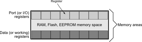
Memory & Registers
Memory is an area where code and instructions are stored.There are normally 3 types of memory present in a microcontroller. These are SRAM, FLASH, and EEPROM memories.
SRAM is the type of memory where data must be read and written to repeatedly. This is the data will change the different code being uploaded to the AVR microcontroller circuit. By default, this is the most common and used type of memory.
Flash memory is the memory that normally stores data that does not change. This is the program memory. It stores the part of the microcontroller program that is fixed and will always stay permanent. This is similar to the BIOS of a general-purpose computer
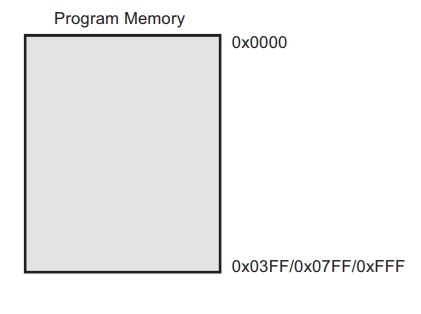
The Flash memory has an endurance of at least 10,000 write/erase cycles. The ATtiny24A/44A/84A Program Counter (PC) is 10/11/12 bits wide, thus addressing the 1024/2048/4096 Program memory locations
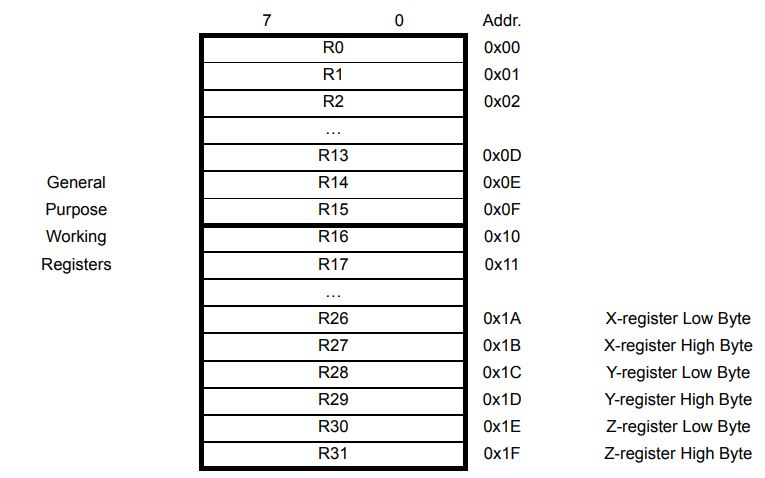
Registers are small memory elements in microcontrollers with 8 bits capacity. Registers can be accessed quickly by the ALU (Arithmetic and Logic Unit) of microcontrollers
source
HELLO-ECHO BOARD
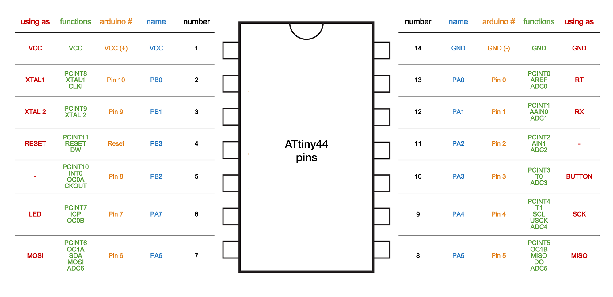
This week we need to program theHello-echo board that we designed in the Electronics Design week. Echo board is based on the Microchip ATtiny44 . It's a 8-bit RISC based microcontroller. The Originla Design have only the UART Port and I added Programmable Button connected to pin PA2 with a Pull-down Resistor and LED connectd toPA3 also it's have 20hz External Resonator.
ATTINY44
The Atmel ATtiny24/44/84 provides the following features: 2/4/8K bytes of in-system programmable flash,
128/256/512 bytes EEPROM, 128/256/512 bytes SRAM, 12 general purpose I/O lines, 32 general purpose working
registers, an 8-bit Timer/Counter with two PWM channels, a 16-bit Timer/Counter with two PWM channels, internal
and external interrupts, an 8-channel 10-bit ADC, programmable gain stage (1x, 20x) for 12 differential ADC channel
pairs, a programmable watchdog timer with internal oscillator, internal calibrated oscillator, and three software
selectable power saving modes
The best Guide to know about a microcontroller and Instruction set it's Datasheet.we will get all the
information from the Datasheet , only problem is it's not a beginner friendly. I started Reading ATtiny44
Datasheet that i got from the Micorchip website. Here you can
download it .
For Six -Wire ISP Programming of ATtiny 44 using six pins shown in below
 source
For Six -Wire ISP Programming of ATtiny 44 using six pins shown in below
- SCK(Serial Clock): Programming clock, generated by the In-System Programmer (Master)
- MOSI(Master Out - Slave In ): Communication line from In-System Programmer (Master) to target AVR being programmed (Slave )
- MISO( Master In - Slave Out ):Communication line from target AVR (Slave) to In- System Programmer (Master)
- RST(Reset):To enable In-System Programming, the target AVR Reset must be kept active. To simplify this, the In-System Programmer should control the target AVR Reset
- GND(Ground):Common Ground
PIN DESCRIPTIONS
- VCC
Supply voltage - GND
Ground - Port B(PB0..PB3)Port B is a 4-bit bi-directional I/O port with internal pull-up resistors (selected for each bit). As inputs, Port B pins that are externally pulled low will source current if the pull-up resistors are activated.so we don't need to add a pull-up resistor externaly for button's and other purpose.
- RESET
Reset input. A low level on this pin for longer than the minimum pulse length will generate a reset, even if the clock is not running.a reset will just reset the programm that currently runnig . - Port A (PA7...PA0)Port A is a 8-bit bi-directional I/O port with internal pull-up resistors (selected for each bit). As inputs, Port A pins that are externally pulled low will source current if the pull-up resistors are activated
Block Diagram
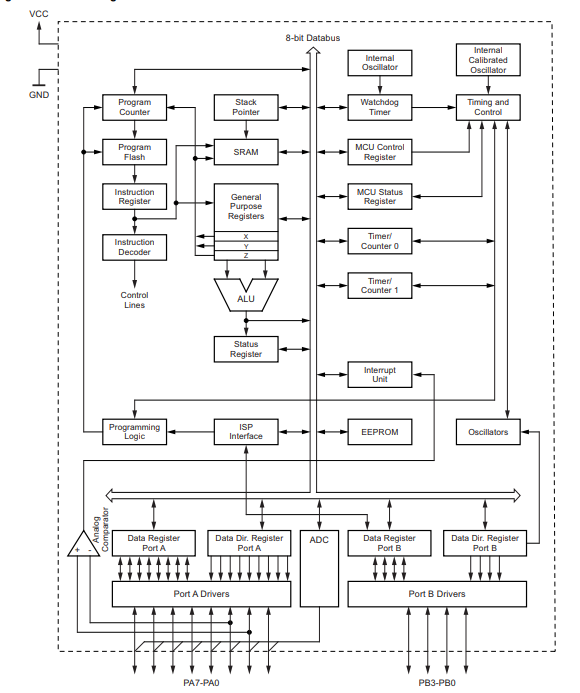
Block Diagram will explain Architecture of the Microcontroller.The AVR uses a Harvard architecture, with separate memories and buses for program and data. Instructions in the program memory are executed with a single-level pipelining. While one instruction is being executed, the next instruction is pre-fetched from the program memory. The ALU supports arithmetic and logic operations between registers or between a constant and a register. Single-register operations can also be executed in the ALU. After an arithmetic operation, the status register is updated to reflect information about the result of the operation.we wil go through all the Stacks when we comes to Progarm the chip.
EMBEDDED PROGRAMMING
There is several ways to progaramme a AVR Microcontroller. Easiest one is using Arduino IDE and there is Microchip Official tool one Atmel Studio also we have toolchain in GCC.First we are using Arduino IDE.We are using the FabTiny ISP as our Progarmmer.
ARDUINO
Arduino is an open-source electronics platform based on easy-to-use hardware and software.ou can tell your board what to do by sending a
set of instructions to the microcontroller on the board. To do so you use the Arduino programming language (based on Wiring), and the Arduino
Software (IDE), based on Processing.Anyone can use Arduino.The Arduino system is based on the avr-gcc compiler and makes use of the standard
AVR libc libraries, which are open-source C libraries, specifically written for Atmel hardware.You can downdload the Arduino IDE
here
Arduino also have Online IDE.
By default the arduino software doesnt contain Attiny 44 chip librarys. We need to include the deatils manually.
In windows we need to install the SPI interface driver
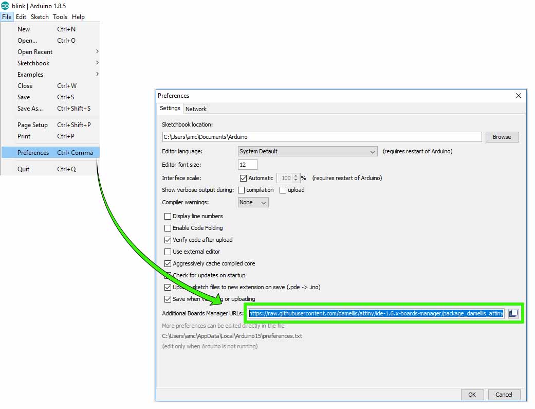
Since the original Arduino software doesnot support the ATtiny44. I have to add some Board directory for adding ATtiny44 board to my arduino enviournment
https://raw.githubusercontent.com/damellis/attiny/ide-1.6.x-boards-manager/package_damellis_attiny_index.json
Pase the above URL in board manager
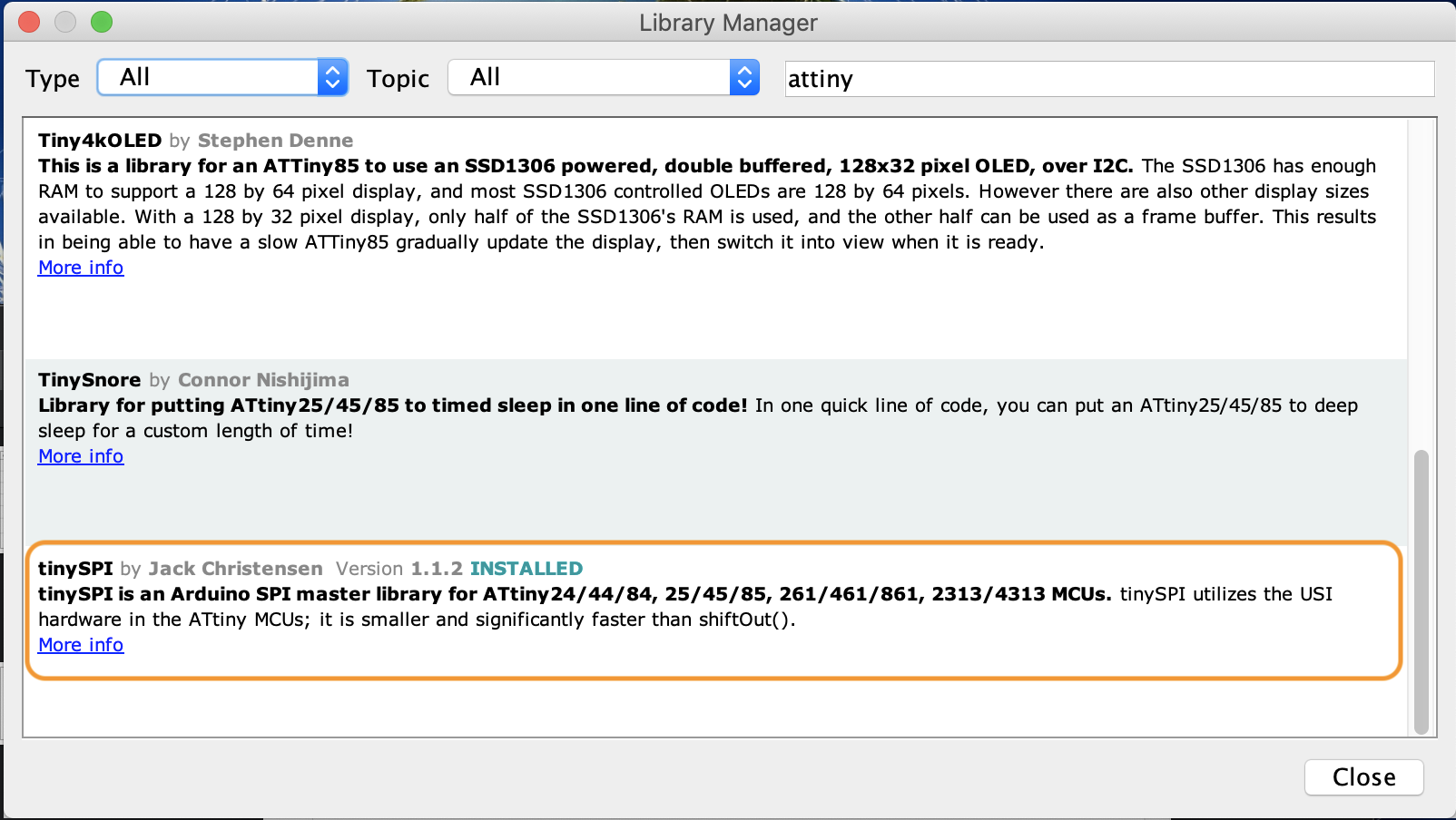
Install the library in library manager.
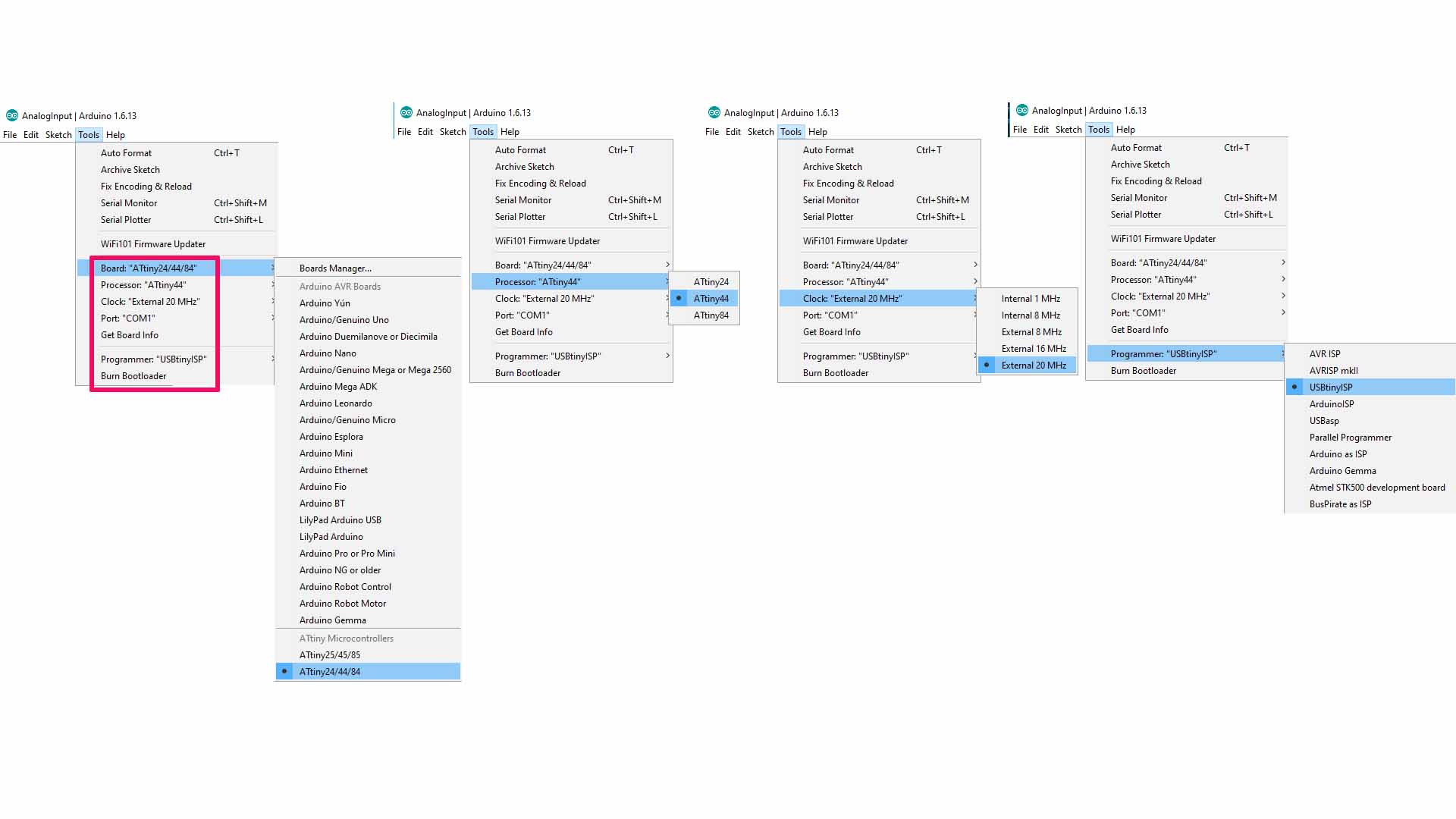
Once the directory is installed, do the following settings.
Select the board as attiny 45.
The inter nal clock of attiny44 is 8mz. I have used an external crytal with frequenzy of 20mz, change the frequenzy in tools.
change the programmer as USBtinyISP
Arduino sketch
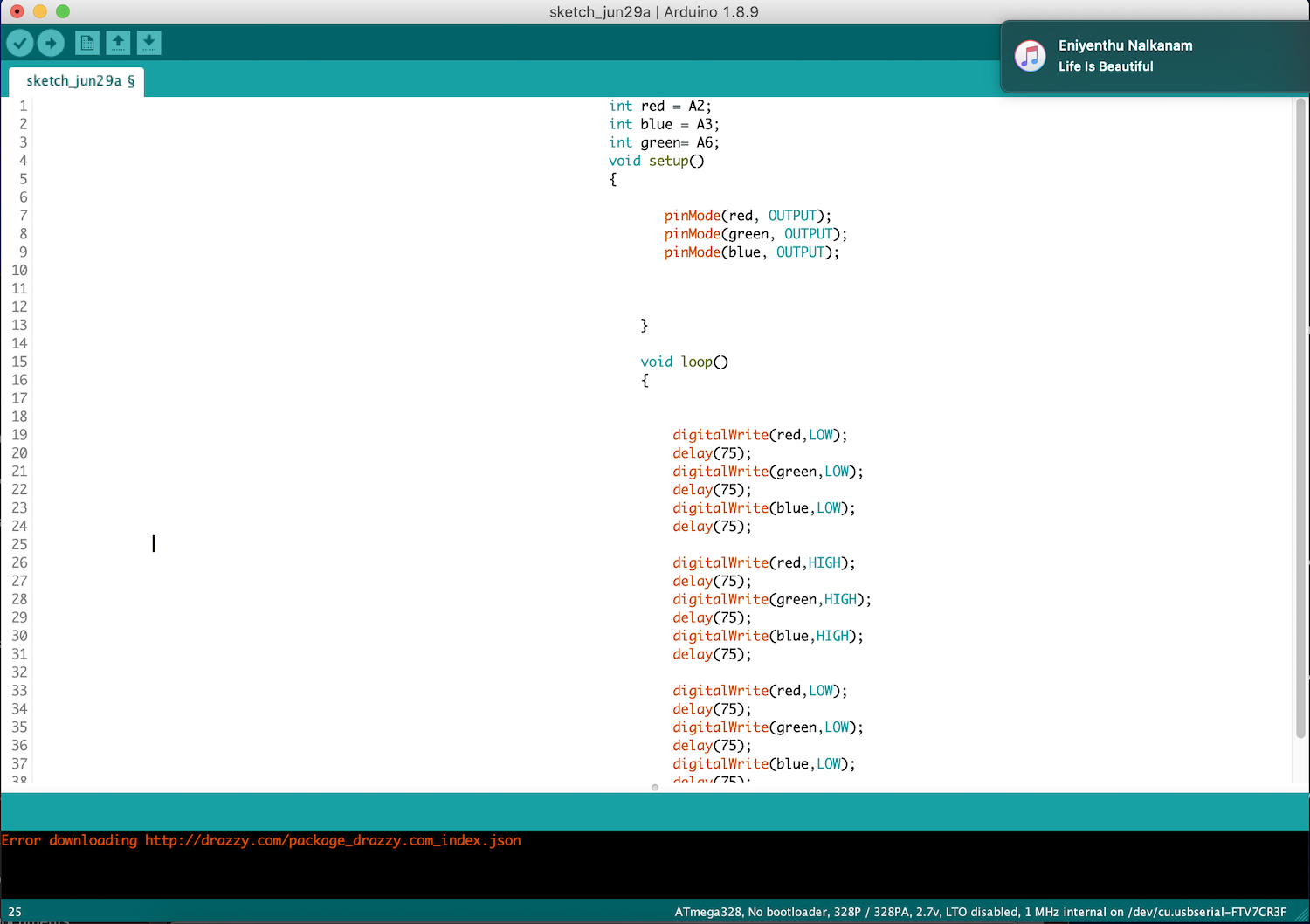
Arduino code
                                                                        int red = A2;
                                                                        int blue = A3;
                                                                        int green= A6;
                                                                        void setup()
                                                                        {

                                                                               pinMode(red, OUTPUT);
                                                                               pinMode(green, OUTPUT);
                                                                               pinMode(blue, OUTPUT);


                                                                            }

                                                                            void loop()
                                                                            {


                                                                                digitalWrite(red,LOW);
                                                                                delay(75);
                                                                                digitalWrite(green,LOW);
                                                                                delay(75);
                                                                                digitalWrite(blue,LOW);
                                                                                delay(75);

                                                                                digitalWrite(red,HIGH);
                                                                                delay(75);
                                                                                digitalWrite(green,HIGH);
                                                                                delay(75);
                                                                                digitalWrite(blue,HIGH);
                                                                                delay(75);

                                                                                digitalWrite(red,LOW);
                                                                                delay(75);
                                                                                digitalWrite(green,LOW);
                                                                                delay(75);
                                                                                digitalWrite(blue,LOW);
                                                                                delay(75);

                                                                                }
Download Code
In the code A2, A3 & A6 are the arduino pin numbers of the IC.
I have given the names for each led the colour.
The delay for each LED is 75 milliseconds.
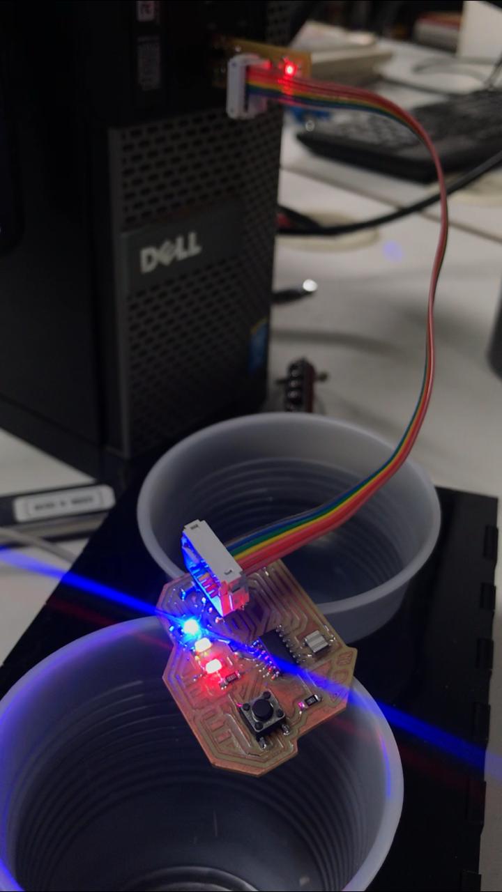
The board is connected to the usb port.
PROGRAMMING ATTINY44 USING ATMEL STUDIO
Studio 7 is the integrated development platform (IDP) for developing and debugging all AVR® and SAM microcontroller applications. The Atmel Studio 7 IDP gives you a seamless and easy-to-use environment to write, build and debug your applications written in C/C++ or assembly code. It also connects seamlessly to the debuggers, programmers and development kits that support AVR® and SAM devices.
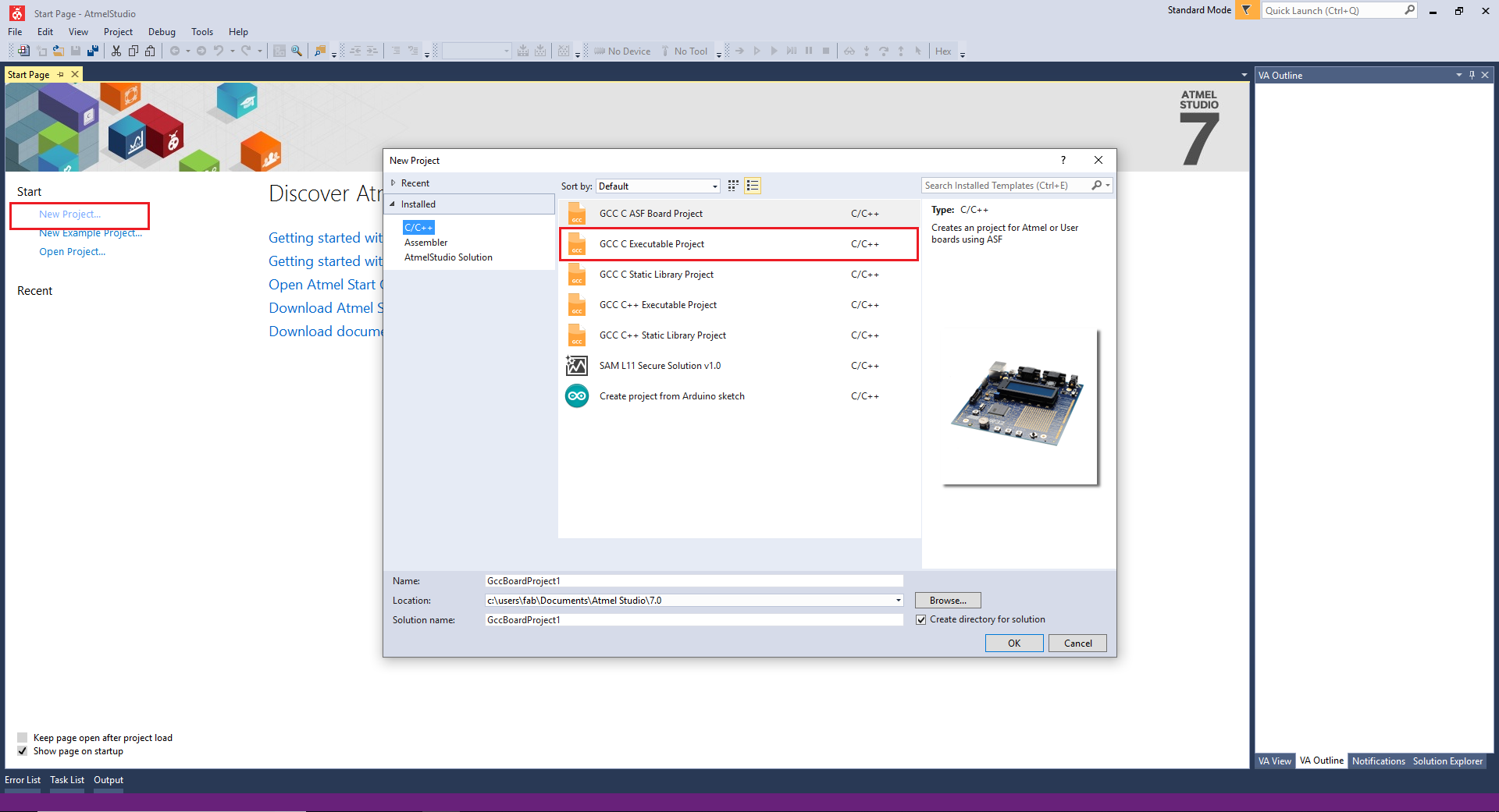
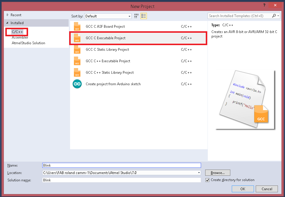
For programming first install and open ATMEL STUDIO. Click "New Project" and select"GCC C Exictable project". Click ok to confirm the selection
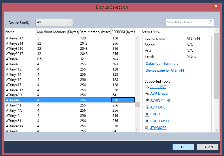
Now you can see the following window. Select device famiy as Attiny and select Attint 44. Click ok to confirm the operation.

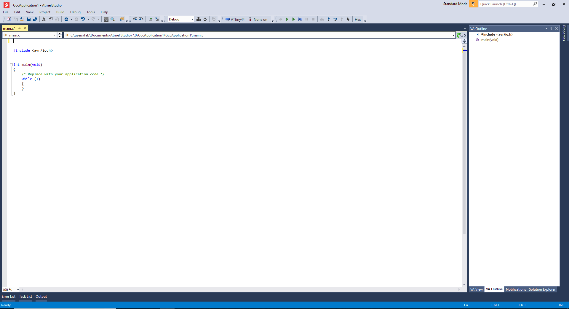
Now you will get a window.
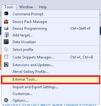
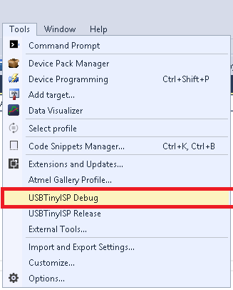
Now we need to setup some parameters for usbtiny debugging. For that Go to "Tools" and Select "External Tools."
Add following details to the box:
DEBUG VERSION
Title:- USBTiny ISP Debug
Command :- avrdude.exe
Arguments :- -c usbtiny -p attiny44 -U flash:w:$(ProjectDir)Debug\$(TargetName).hex:i
click apply and ok to save the tool.
RELEASE VERSION
Title:- USBTiny ISP Release.
Command :- avrdude.exe
Arguments :- -c usbtiny -p attiny44 -U flash:w:$(ProjectDir)Release\$(TargetName).hex:i
click apply and ok to save the tool.
Start a Project by clicking File >> New >> Project
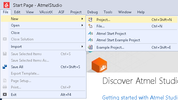
Now select C/C++ as language and Template as GCC C Executable Project give a name and click OK.
Then Select the Target Microcontroller , in here we have ATtiny44.
    #define F_CPU 20000000UL      //Clock 20-Mhz
                                                                #include


                                                                int main(void)
                                                                {

                                                                  DDRA |= (1 << 2);   // Set PA2 as OUTPUT for Red led
                                                                  DDRA |= (1 << 3);  // Set PA3 as OUTPUT for Yellow led
                                                                  DDRA |= (1 << 4); // set PA4 as OUPUT for Blue led


                                                                  DDRA &= ~ (1 << 7);   //Set PA2 as INPUT for Button


                                                                  while (1)
                                                                  {
                                                                    if (PINA & (1 << 2)) //check whether the button pressed or not
                                                                    {
                                                                      PORTA = PORTA | (1 << 2); // Turn on Red led
                                                                      PORTA = PORTA | (1 << 3); // Turn on Yellow led
                                                                      PORTA = PORTA | (1 << 4); // Turn on Blue led


                                                                    }
                                                                    else
                                                                    {
                                                                      PORTA &= ~(1 << 2);   // Turn on RED led
                                                                      PORTA &= ~(1 << 2);   // Turn on Yellow led
                                                                      PORTA &= ~(1 << 2);   // Turn on Blue led
                                                                    }

                                                                  }
                                                                }
For Uploading code first we need to build/compile it by using Build > Build Soution
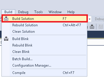
After the compailation we need to flash the code in to our board
Group assignment
In this week group assignment is to try out some other acchtecture other than AVR microcontrollers.
ARM (Advanced RISC Machines)There would be a very small segment of the mobile community that would not have heard anything about the Android OS by Google. This OS seems to be giving many proprietary vendors a run for their money and the owners many a sleepless nights. But did you know as to what does android depend on for its good performance apart from its robust code? What makes it run so smooth and yet amazingly fast without costing you a fortune? What drives the Android? The answer is ARMs, Advanced RISC Machines, previously known as Acorn RISC Machines.
ARM machines have a 32 bit Reduced Instruction Set Computer (RISC) Load Store Architecture. (Also read article on CISC & RISC Architecture) The relative simplicity of ARM machines for low power applications like mobile, embedded and microcontroller applications and small microprocessors make them a lucrative choice for the manufacturers to bank on. The direct manipulation of memory isn’t possible in this architecture and is done through the use of registers. The instruction set offers many conditional and other varieties of operations with the primary focus being on reducing the number of cycles per instruction featuring mostly single cycle operations.
All instructions in the ARM ISA are conditional with the normal execution instructions also being accompanied by condition AL. There are 14 conditions available excluding AL. The instruction set added many feathers to its cap as and when the generations grew. The transistor count has also increased substantially from 30000 in ARM2 to about 26 million in Cortex-A9 ARM. An additional Thumb architecture was developed to support 16-bit instruction models on the otherwise 32 bit ARM machines. No matter the added advantage of increased code density which was about 65% of the original ARM code, this resulted in a little performance drop in the ARM machines. This drop was somewhat balanced with Thumb 2 which was a major extension over the Thumb ISA.
GARM Architecture
In Thumb 2, the compiler automatically selects a mixture of 16 bit and 32 bit instructions. It is to be noted that only the instruction set changes from 32 bit to 16 bit, the core continues to operate at 32 bit. The evolution of ARM v7 cores saw the development of Thumb Execution Environment (Thumb-EE) which offered dynamic coding by compiling the code moments before or during execution itself. Thumb feature is basically another Instruction Set running on the same platform. Another Instruction set, to execute Java codes on ARMs was developed soon and was named Jazelle. These three Instruction sets are now the three states on an ARM core and to shift from one state to another, directives like ARM, THUMBX and THUMB are given to the assembler. The evolution of ARM architectures is shown in the figure below:
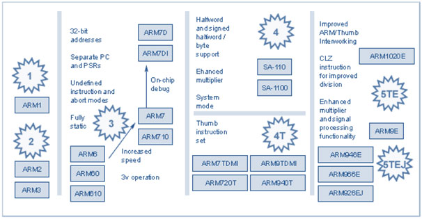
The nomenclature of ARMs is based on the type and features used in it. For example in ARM7TDMI, ‘T‘ stands for Thumb, ‘D’ and ‘I’ together comprise the on chip debugging facilities and ‘M’ signifies support for an enhanced multiplier and support for 64-bit results. ARMx7z like the ARM1176JZ-S indicates AXI bus, physically mapped caches and MMU, has version 6Z architecture. In this way, there is a naming convention for ARM devices. ARM architectures used various stages of pipelining to enhance the flow of instructions to the processors. This allows several operations to be performed simultaneously which would otherwise be performed serially. For example, the ARM7TDMI used 3 stages, ARM9TDMI uses 5 stages and the ARM10TDMI use 6 stages of pipeline to speed up delivery and faster clocking. Cores up to ARM7 followed a Von Neumann type architecture which is essentially memory mapped architecture. ARM9 and its successors shifted to Harvard Architecture which is port mapped. They also provide a robust debugging environment like the Embedded ICE Logic which connects with the external world through a Test Access Port or a standard IEEE 1149.1 JTAG connection. This helps shorten the development cycle.
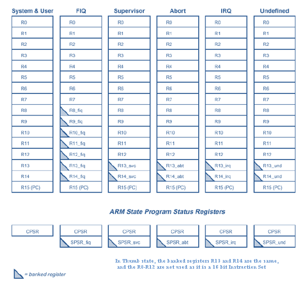
ARM Registers
In general ARMs have 37 registers arranged in partially overlapping banks, with separate register banks for each processor mode thus providing rapid context switching for special operations. The various modes in an ARM can be summarized in the figure below.
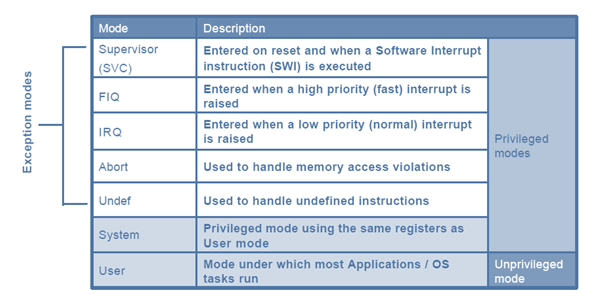
Each register is 32 bits in size.
The registers are roughly divided into:
- 30 General Purpose Registers: Only 15 GPRs are visible any one time depending on the mode of operation and are numbered R0-R12, Stack Pointer and Link Register. While the stack pointer is essentially used by the compliers like those of C/C++, its use as any other GPR is deprecated. Link register stores return addresses in subroutines or exceptions depending on the mode of operation.
- Program Counter: Loads the address of destinations on branching operations and may be manually set while doing subroutine calls.
- Application Program Status Register: It contains a copy of flags from the ALU to check if the conditional instructions were executed.
- Current Program Status Register: It holds various information regarding APSR, current processor mode, interrupt flags, execution state bits etc.
- Saved Program Status Register: In case an exception is detected, this register holds the values of the CPSR.
Classification of Instruction Set
The ARM and Thumb instruction sets can be broadly classified into the following functional groups.
- Branching and Control Instructions: Instructions like subroutine calls, looping and changing the state between ARM and Thumb fall under this category of instructions.
- Register Load and Store instructions: Loading the values of single registers to and from the memory are covered under this type of instructions. The values may be 32 bit word, a 16-bit half word or an 8 bit unsigned value.
- Multiple Register Load and Store Instructions: Facilitate the to and fro movement between the contents of the multiple registers, used in block operations and stack operations.
- Data Processing Instructions: Operations like addition, subtraction or bitwise logic on the contents of the registers are performed by this type of instructions.
- Status Register access Instructions: These instructions primarily move the contents between the status registers and the GPRs.
- Coprocessor Instructions: These provide a general framework to extend the ARM architectures.
 Source:https://www.engineersgarage.com/articles/arm-advanced-risc-machines-processors
STM32
STM32 is a family of 32-bit microcontroller integrated circuits by STMicroelectronics. The STM32 chips are grouped into related series that are based around the same 32-bit ARM processor core, such as the Cortex-M7F, Cortex-M4F, Cortex-M3, Cortex-M0+, or Cortex-M0. Internally, each microcontroller consists of the processor core, static RAM memory, flash memory, debugging interface, and various peripherals.
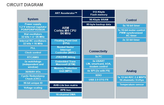
In here Fablab Kochi we have the STM32F401 series Nucleo development boards.it's a part of the STM32 Dynamic Efficiency™ device range. These devices offer the best balance of dynamic power consumption (in run mode) and processing performance, while integrating a high number of added-value features in packages as small as 3 x 3 mm.
The MCUs deliver the performance of Cortex®-M4 core with floating point unit, running at 84 MHz, while achieving outstandingly low power consumption values in run and stop modes.
- Performance: At 84 MHz, the STM32F401 delivers 105 DMIPS/285 CoreMark performance executing from Flash memory, with 0-wait states using ST’s ART Accelerator. The DSP instructions and the floating point unit enlarge the range of addressable applications.
- Power efficiency: ST’s 90 nm process, ART Accelerator and the dynamic power scaling enables the current consumption in run mode and executing from Flash memory to be as low as 128 µA/MHz. In Stop mode, the power consumption can be as low as 9 µA.
- Integration :The STM32F401 portfolio provides from 128 to 512 Kbytes of Flash, 96 Kbytes of SRAM. The available packages range from 49 to 100 pins.
- 3x USARTs running at up to 10.5 Mbit/s,
- 4x SPI running at up to 42 Mbit/s,
- 3x I²C,
- 1x SDIO,
- 1x USB 2.0 OTG full speed,
- 2x full duplex I²S up to up to 32-bit/192KHz,
- 12-bit ADC reaching 2.4 MSPS,
- 10 timers, 16- and 32-bit, running at up to 84 MHz
You can download the sheet from here