7. Electronics design
Group assignment
Individual assignment
Week 07 - Electronics design
Kicad setup
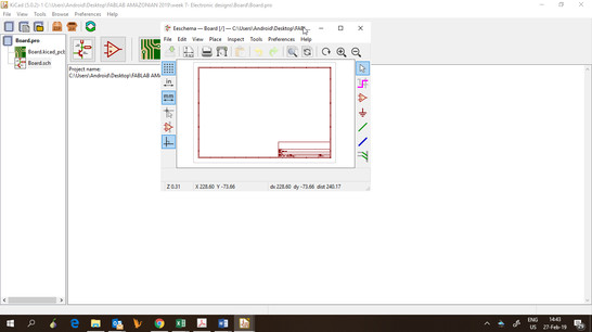
I decided to use KiCAD as electronics design software. Link to KiCAD.
After starting a new project, the fab libraries with symbols and footprints must be included.
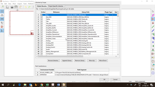
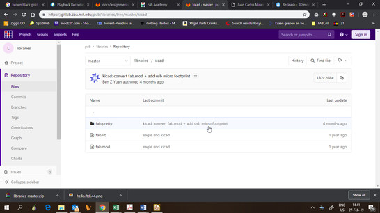
Link to FabAcademy libraries.
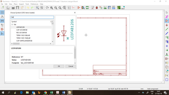
Then, all the components symbols must be added to the schematic editor. These components are the same as Neil’s design.

To add a new symbol form the fab library, I used the search bar, then all the components needed are easier to find.
Following Neil’s design, I made all the connections on the schematic editor
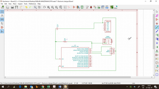
Then, I added an LED in series with a resistor connected between PB2 and GND. Also a button with a pull-down resistor to PA3.
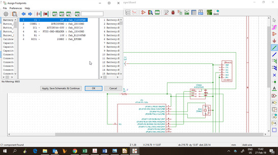
When all the connections are finished, these steps must be followed:
- Annotate schematic symbols.
- Assign PCB footprints.
- Generate netlist.
- Run Pcbnew.
The correct footprint must be assigned to each component before designing the PCB. This means choosing the name of the footprint that matches the symbol name.
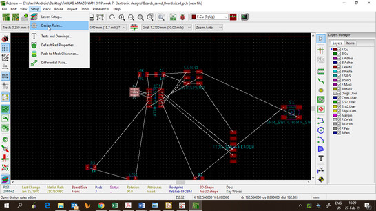
Before designing the PCB, the design rules must be defined. For my board I set the Track width to 0.35 and the Clearance to 0.25.
When designing the PCB, the footprints must be arranged exactly the way they will be milled on the PCB.
First, the components are moved to the desired position, then the traces are drawn. Sometimes this process must be repeated to achieve a better distribution.
Again I followed Neil’s design, and then arranged the components that I added.
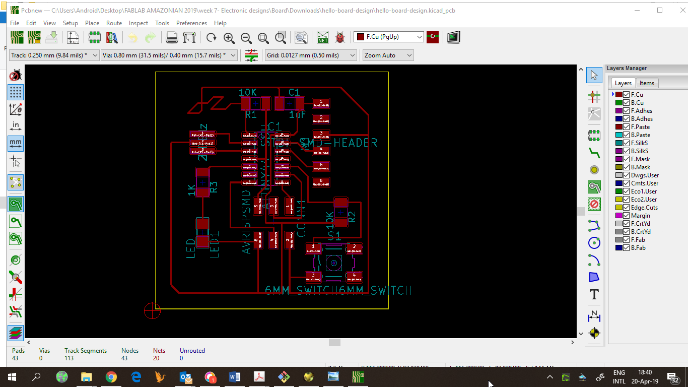 This was the end result and i am ready to mill.
Board design
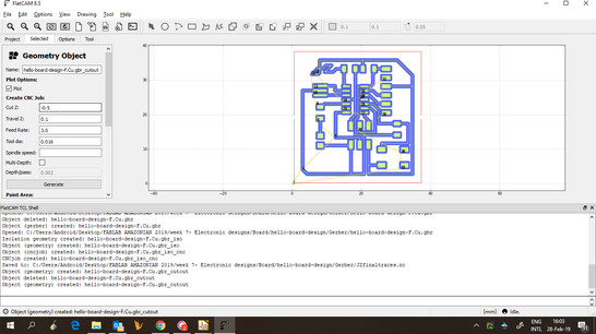
When the PCB design is ready, the gerber files are created, and then I used FlatCAM to create the gCode from the gerber files.
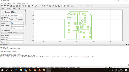
The parameters for FlatCAM are:
- Tool dia: 0.4
- # passes: 3
- Pass overlap: 0.3
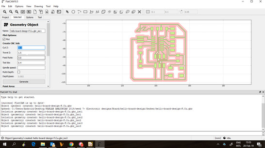
Then:
- Cut Z: -0.15
- Travel Z: 1.5
- Feed rate: 1
- Spindle speed: 2000
For the cut gCode, the tool diameter changes to 0.8 and the cut z to -1.5 in three steps.

Heroshot:
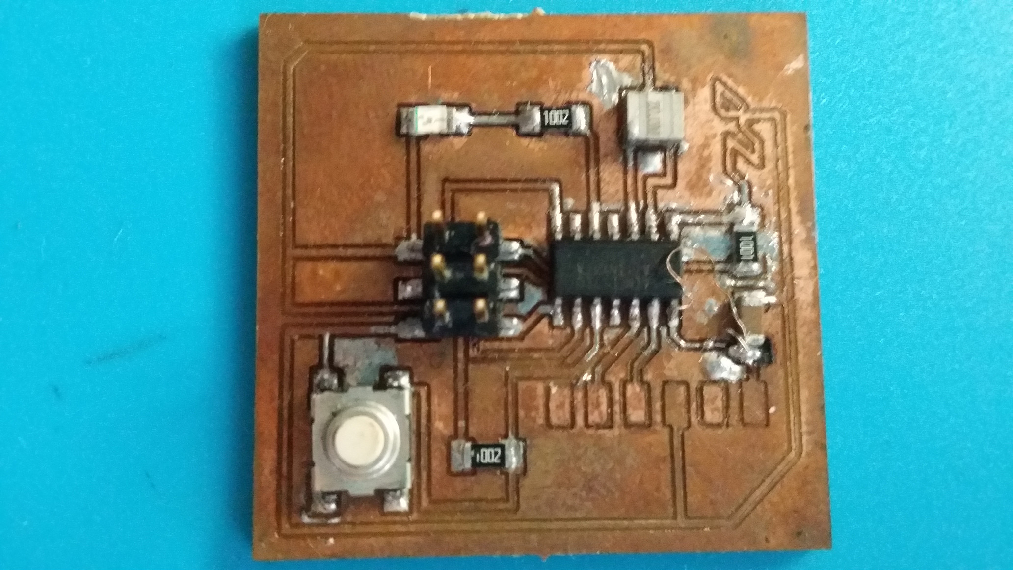
This was the end result after soldering the board,this picture is an older picture I got a failure on the board and a trace got burned
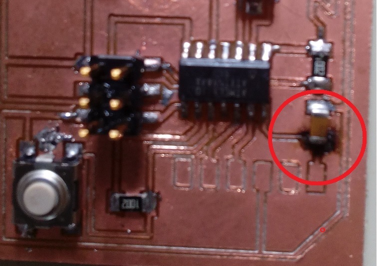
because we run out of milling bits i could not remake the board and i had to make a bridge waiting for new bits The bridge was made from the capacitor to the first pin of the controller :(
Programming the board
To program the board, I first installed the usbTinyISP programmer driver for windows from this link.
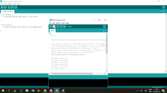
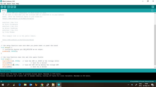
To test the board, I used the Blink example from Arduino, but had to change the led pin number to 8.
Then, I change the board to ATTiny44 with 20MHz external clock and the programmer to USBTinyISP.
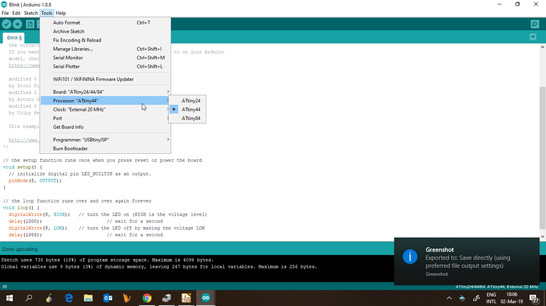
And the LED blinked.